Note: Descriptions are shown in the official language in which they were submitted.
CA 02785959 2012-08-13
A SOFC STACK HAVING A HIGH TEMPERATURE BONDED CERAMIC INTERCONNECT
AND METHOD FOR MAKING SAME
TECHNICAL FIELD
In pursuit of high-efficiency, environmentally friendly energy production,
solid oxide fuel cell
(SOFC) technologies have emerged as a potential alternative to conventional
turbine and combustion
engines. SOFCs are generally defined as a type of fuel cell in which the
electrolyte is a solid metal oxide
(generally non-porous or limited to closed porosity), in which 02" ions are
transported from the cathode
to the anode. Fuel cell technologies, and particularly SOFCs, typically have a
higher efficiency and have
lower CO and NOx emissions than traditional combustion engines. In addition,
fuel cell technologies tend
to be quiet and vibration-free. Solid oxide fuel cells have an advantage over
other fuel cell varieties. For
example, SOFCs can use fuel sources, such as natural gas, propane, methanol,
kerosene, and diesel,
among others, because SOFCs operate at sufficiently high operating
temperatures to allow for internal
fuel reformation. However, challenges exist in reducing the cost of SOFC
systems to be competitive with
combustion engines and other fuel cell technologies. These challenges include
lowering the cost of
materials, improving degradation or life cycle, and improving operation
characteristics, such as current
and power density.
Among the many challenges with the manufacture of SOFCs, the formation of free
standing and
fully integrated SOFC stacks parameters remains a notable engineering hurdle,
particularly, SOFC stacks
utilizing a series electrical connection, or SOFC stacks utilizing a variety
of different materials with
different processing. In this respect, prior art techniques have focused on
processing individual
component layers or a plurality of layers having similar processing parameters
combined with a final
joining process to bond all of the components to form a SOFC stack. The final
joining process usually
involves bonding the individual layers or cells together using a solder or
glass encapsulant and entails
multiple firing cycles. Often the layers and the cells are merely clamped
together and held under pressure.
In view of the foregoing, the industry continues to have a need for improved
SOFC cells and SOFC cell
stacks.
SUMMARY OF THE INVENTION
The present invention is directed to an integrated SOFC stack. The stack
includes a first cell
having a cathode layer, an electrolyte layer overlying the cathode layer, and
an anode layer overlying the
electrolyte layer. A second cell has a cathode layer, an electrolyte layer
overlying the cathode layer, and
an anode overlying the electrolyte layer. A ceramic interconnect layer is
between the first cell and the
- 1 -
CA 02785959 2012-08-13
second cell. The ceramic interconnect layer has a first high temperature
bonding region along an
interfacial region between the first cell and the ceramic interconnect layer,
and a second high temperature
bonding region along an interfacial region between the second cell and the
ceramic interconnect layer.
A method for forming an integrated SOFC stack includes forming a first cell
structure. The first
cell structure has a first electrode layer, an electrolyte layer overlying the
first electrode layer, and a
second electrode layer overlying the electrolyte layer. A ceramic interconnect
layer overlying the first cell
structure is formed. A second cell structure is formed. The second cell
structure has a first electrode layer,
an electrolyte layer overlying the first electrode layer, and a second
electrode layer overlying the
electrolyte layer. The first cell structure, the interconnect layer, and the
second cell structure are hot
pressed together to integrally bond the first cell structure, the interconnect
layer and the second cell
structure to form an integrated SOFC cell stack.
Another method for forming an integrated SOFC component includes forming a
first green cell
structure having a first green electrode layer, a green electrolyte layer
overlaying the first green electrode
layer, and a second green electrode layer overlaying the green electrolyte
layer. A second green cell
structure is formed having a first green electrode layer, a green electrolyte
layer overlaying the first green
electrode layer, and a second green electrode layer overlaying the green
electrolyte layer. A green ceramic
interconnect layer is formed disposed between the first green cell structure
and the second green cell
structure. The first green cell structure, the green ceramic interconnect
layer, and the second green cell
structure are hot pressed together to integrally bond the first green cell
structure, the green ceramic
interconnect layer and the second green cell structure to form an integrated,
densified SOFC cell stack.
An integrated SOFC stack includes a first cell having a first cathode layer, a
first electrolyte layer
overlying the first cathode layer, and a first anode layer overlying the first
electrolyte layer. A second cell
has a second cathode layer, a second electrolyte layer overlying the second
cathode layer, and a second
anode overlying the second electrolyte layer. An interconnect layer is between
the first cell and the
second cell. The interconnect layer is directly fused to either said first
cathode layer or first anode layer of
said first cell, and the interconnect layer is directly fused to either the
second cathode layer or second
anode layer of the second cell.
An integrated SOFC stack includes a first cell having a cathode layer, an
electrolyte layer
connected to the cathode layer, and an anode layer connected to the
electrolyte layer. A second cell has a
cathode layer, an electrolyte layer connected to the cathode layer, and an
anode connected to the
- 2 -
CA 02785959 2012-08-13
electrolyte layer. An interconnect layer is between the first cell and the
second cell. The interconnect layer
is bonded to the first cell and to the second cell in the absence of
encapsulants and bonding agents.
A method for making an integrated SOFC stack includes forming a first cell
structure. The first
cell structure includes a first electrode layer, a first electrolyte layer
overlying the first electrode layer, and
a second electrode layer overlying the first electrolyte layer. A ceramic
interconnect layer is formed
overlying the first cell structure. A second cell structure formed to include
a third electrode layer, a
second electrolyte layer overlying the third electrode layer, and a fourth
electrode layer overlying the
second electrolyte layer. The first cell structure, the interconnect layer,
and the second cell structure are
hot pressed together to integrally bond the first cell structure to the
interconnect layer and the second cell
structure to the interconnect layer, thereby forming an integrated SOFC cell
stack.
BRIEF DESCRIPTION OF THE DRAWINGS
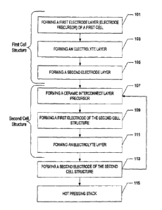
FIG. 1 illustrates a process flow according to an embodiment of the present
invention.
FIG. 2 illustrates a SOFC stack according to an embodiment of the present
invention.
The foregoing and other objects, features and advantages of the invention will
be apparent from
the following more particular description of preferred embodiments of the
invention, as illustrated in the
accompanying drawings in which like reference characters refer to the same
parts throughout the different
views. The drawings are not necessarily to scale, emphasis instead being
placed upon illustrating the
principles of the invention. All parts and percentages are by volume unless
otherwise indicated.
MODES FOR CARRYING OUT THE INVENTION
According to one embodiment, a method for making a SOFC stack is provided and
may be
produced according to a process flow illustrated in FIG. 1. An SOFC stack
typically includes one or more
SOFC cell structures, which generally include a cathode, anode, and interposed
electrolyte. At step 101, a
first electrode layer (electrode precursor) of a first cell is formed. The
first electrode layer may include an
anode or a cathode material. According to one embodiment, the first electrode
is a cathode formed of a
ceramic oxide material or precursor thereof. According to a particular
embodiment, the cathode layer
material includes lanthanum and manganese, and may further include strontium,
forming a cathode
commonly referred to as LSM (lanthanum strontium manganate).
Alternatively, the first electrode layer may be an anode material, such as a
cermet, that is a
material having a ceramic phase and a metal phase, or a precursor thereof. The
ceramic phase may
- 3 -
CA 02785959 2012-08-13
include zirconia and the metal phase may include nickel. In particular, the
ceramic zirconia phase of the
anode material is a stabilized zirconia material such as yttria stabilized
zirconia (YSZ). The nickel is
generally produced through the reduction of nickel oxide included in the anode
precursor material, such
as a green ceramic composition that is heat-treated.
Additionally, the final-formed electrodes of the SOFC cell structures, either
the anode or the
cathode, generally have a high volume of porosity to allow transport of
gaseous species used to fuel the
oxidation/reduction reaction of the fuel cell. According to one embodiment,
the percent porosity of the
final-formed electrodes in the fuel cell structures is not less than about
15.0 vol%, such as not less than
about 20 vol%, about 30 vol%, about 50 vol%, or not less than about 70 vol%.
Still, the percent porosity
of the electrodes of the cell structures is particularly within a range of
between about 15 vol% and
70 vol%.
Generally, the final-formed electrodes (anodes and cathodes) of the SOFC cell
structures have a
thickness of not less than about 1.0 mm. According to one embodiment, the
thickness of the electrodes is
greater, such as not less than about 1.5 mm, or not less than about 2.0 mm, or
even not less than about 5.0
mm. Still, the thickness of the electrodes is limited and is generally not
greater than about 50 mm.
In another embodiment, channels can be formed within the electrodes to
facilitate better gas
delivery to and removal from the electrodes. There exists a variety of
possible materials such that fibers
can be used to form the channels or passageways within the cathode and anode
layers.
Generally, the only limitations on the selection of materials would be that
the material would burn
or be out-gassed from the fuel cell during the firing process, and that the
material is not reactive with the
ceramic particles. These two conditions are adequately satisfied by organic
based materials. Thus, the
fibers can be natural fibers; cotton, bast fibers, cordage fibers, or animal
fibers, such as wool, or they may
be manufactured fibers; regenerated cellulose, cellulose diacetate, cellulose
triacetate, polyamide,
polyester, polyacrylic, polyvinyl, polyolefin resins, carbon or graphite
fibers, or liquid crystal polymers.
Alternatively, the fibers can be extruded lengths of binder material such as
synthetic rubber,
thermoplastics, or polyvinyl and extruded lengths of plasticizer material such
as glycol and phthalate
groups. In another embodiment, the material can be pasta, such as spaghetti.
Alternatively, gas channels can be formed into the green electrodes layer
without employing any
fiber or material to be burned out during sintering. The channels can be
formed by pressing, molding, or
other suitable means known in the art.
- 4 -
CA 02785959 2012-08-13
The average size of the channels within the final-formed electrodes is
generally greater than about
0.5 mm to reduce pressure drop. In one embodiment, the average size of the
channels is greater than about
0.7 mm, such as greater than about 1.0 mm, or even greater than about 2.0 mm.
Typically, the average
size of the channels within the electrodes is within a range between about 0.5
mm and about 2.0 mm and
more particularly within a range between about 0.7 mm and about 1.5 mm.
In further reference to one method for forming an SOFC stack, as illustrated
in FIG. 1, forming a
first cell structure also includes forming an electrolyte layer precursor, at
step 103. Suitable materials for
the electrolyte layer of the cell structures include ceramic oxides, such as
zirconia, ceria, gallia, and other
known ionic conductors. Oxygen ion conductivity may be enhanced with oxide
stabilizer materials such
as yttrium, scandium, samarium, ytterbium and gadolinium. Suitable stabilizing
materials include oxides
such as Ti02, Ce02, CaO, Y203, MgO, Sc203, In203, and Sn02. For example, the
electrolyte layer
may be formed from yttria-stabilized zirconia, scandia-doped zirconia,
ytterbia-doped zirconia, samarium
oxide-doped ceria, gadolinium oxide-doped ceria, or calcia-doped ceria, among
others.
Forming the first cell structure according to a particular embodiment
illustrated in the flow chart
of FIG. I is completed by forming a second electrode layer, at step 105.
Accordingly, the second
electrode of the first cell structure involves forming either a cathode or an
anode, depending upon which
type of electrode was previously formed as the first electrode. As such the
first cell structure includes a
cathode, an anode and an electrolyte layer disposed between the anode and
cathode.
According to FIG. 1, the formation of a SOFC stack further includes forming a
ceramic
interconnect layer precursor, at step 107. Generally, the ceramic interconnect
layer provides an electrical
connection between the two adjacent cells and, unlike in parallel SOFC stack
formations, the ceramic
interconnect layer facilitates series connection of cells. Suitable materials
for forming the ceramic
interconnect layer may include chromium. Additionally, chromium-containing
ceramic materials may
further include rare earth elements, such as doped rare earth chromites.
According to one embodiment, the
ceramic interconnect layer includes materials such as lanthanum, strontium,
calcium, cobalt, gallium,
yttria, titanate, and magnesium. In one particular embodiment, the species of
the interconnect layer can
include ceramics such as LaSrCr03, LaMgCr03, LaCaCr03, YCr03, LaCrOs1 LaCo03,
CaCr03,
CaCo03, LaNi03, LaCr03, CaNi03, and CaCr03
Typically, the final-formed ceramic interconnect layer generally has an
average thickness of less
than about 100 microns. Other embodiments utilize a thinner ceramic
interconnect layer, such that it has
an average thickness of less than about 50 microns, such as less than about 20
microns, or even less than
- 5 -
CA 02785959 2013-03-12
about 15 microns. Still, the average thickness of the final-formed ceramic
interconnect layer is limited,
such that it is not less than about 1.0 micron.
In further reference to one method for forming an SOFC stack outlined in the
flow chart of FIG.
1, the process continues with the formation of a first electrode of the second
cell structure, at step 109, the
formation of an electrolyte layer at step 111, and the formation of a second
electrode of the second cell
structure at step 113. The second cell structure, like the first cell
structure, includes an anode, cathode and
interposed electrolyte layer. As such, the second cell structure generally has
a substantially similar, if not
identical, structure and composition as that of the first cell structure.
Generally, the cathode, anode, and electrolyte materials are the same as those
used in making the
component layers of the first cell structure. The formation of multiple cell
structures with an interposed
ceramic interconnect layer can be repeated, to form 3, 4, 5, 6 or greater cell
stacks.
After the formation of a first and second cell structure with an interposed
ceramic interconnect
layer, the component layers are hot pressed together, as shown in step 115, to
form an integrally bonded
SOFC stack including the first cell, the ceramic interconnect layer, and the
second cell. The integrally
bonded SOFC is made into a whole by bringing all layers together and unifying
them.
Generally, the hot pressing technique involves an applied uniaxial pressure
through use of a
piston, to aid densification of the component layers. In one embodiment, the
maximum pressure during
formation of the SOFC stack is not less than about 0.5 MPa, such as not less
than about 3.0 MPa, 5.0
MPa, or 8.0 MPa. The peak pressure utilized during hot pressing may vary, such
as within a range of
about 0.5 to 10.0 MPa, such as 1.0 to 5.0 MPa. Further, an applied temperature
during pressing aids in the
densification of the layers. The temperature applied during hot pressing is
not less than about 1,050 C,
such as not less than about 1,000 C, 1,100 C, or 1,200 C. In addition, the
temperature applied during hot
pressing may not be greater than about 1,800 C such as not greater than about
1,700 C, or 1,600 C, and
as such, the maximum temperature during hot pressing may be within a range of
between about 1,100 C
and about 1,700 C. In one embodiment, single cells and multiple cell stacks
may be hot pressed at a
heating rate of 1 C/min. to 100 C/min. Pressing may be carried out on the
order of 10 min. to 2 hours,
such as 15 mm. to 1 hour. Particular embodiments were hot pressed for 15 to 45
min.
Heat treatment may be performed in a reducing atmosphere or, preferably in a
non-reducing
atmosphere, such as an oxidizing atmosphere. If heat treatment is performed in
a reducing atmosphere, a
subsequent oxidation step can be performed. The oxidation step can be used to
remove channel formers
and pore formers. The oxidation can result in the oxidation of some nickel
within the anode or nickel
- 6 -
CA 02785959 2013-03-12
within wire mesh in various electrodes. As such, a subsequent reduction step
can be performed. However,
hot pressing in an oxidation atmosphere can reduce the number of additional
oxidation and reduction
steps. Further, the hot pressing can take place without the aid of a
restraining die.
The starting ceramic materials for the electrodes (anode and cathode) and
electrolytes (electrolyte
layer and interconnect layer) can be in powder form having an average diameter
of about one micron.
Each of the materials for a component of the stack is calcined (partial
sintering) isobarically while not
under pressure. After calcining, the resulting calcined blocks are crushed by
suitable means known in the
art, such as ball milling, to form powders. The powders are screened to
desired size ranges. For example,
the calcined powder, such as LSM, for a cathode base layer can be screened to
a mesh size range of
greater than about 75 microns but less than about 106 microns. For a cathode
functional layer, the
calcined powder can be screened to a mesh size range of greater than about 25
microns but less than about
45 microns.
Alternatively, the interlayer forming the cathode functional layer may be
formed of a largely
unagglomerated powder, having a notably fine particle size. For example,
average particle size can lie
within a range of about 0.1 gm to about 10 gm. Typically, the average particle
size of the relatively fine
material is not greater than about 5 gm. A powder having an average particle
size within a range of about
0.5 gm to about 5 gm can be particularly suitable.
For the anode base layer and the anode functional layer, the calcined powders,
such as
YSZ/nickel oxide, can be screened to a mesh size range of less than about 150
microns and about 45
microns, respectively. An electrode having a functional layer and base layer
are usually formed of the
same material and have a bimodal grain size distribution or a bimodal pore
size distribution.
Similarly to the cathode functional layer, the anode functional layer may
alternatively be formed
of a largely unagglomerated powder, having a notably fine particle size. For
example, average particle
size can lie within a range of about 0.1 gm to about 10 gm. Typically, the
average particle size of the
relatively fine material is not greater than about 5 gm. A powder having an
average particle size within a
range of about 0.5 gm to about 5 gm can be particularly suitable.
Electrode configurations are further described in United States Publication
No. 2007/0237999, published
on October 11, 2007, and International Publication No. WO/2007/118127,
published on October 18, 2007.
- 7 -
CA 02785959 2012-08-13
Additionally, the powders used to form the electrodes can include powders
having spherical
particles or non-spherical particles, such as elliptical, needle-shaped, or
irregularly shaped particles, or a
combination of spherical and non-spherical particles. In particular reference
to non-spherical particles,
such particles typically have a largest dimension, which for the purposes of
this discussion will be
referred to as the length, and accordingly, the length of such non-spherical
particles is the same as the
mesh sizes described above.
Generally, the final formed electrodes have a volume density of not greater
than about 80%. In
particular, the electrodes can have a lesser volume density, such as not
greater than about 75%, or not
greater than about 70%, or even about 65% or less. Notably, such low densities
(high porosities) are
achieved without the use of pore formers. The resulting pores are formed in
situ during processing and
have an average size on the order of average grain size and smaller. Pore
shapes are irregular, in contrast
to pore former-based pores, which tend to be spherical or otherwise regularly
shaped.
The electrolyte and interconnect powders can be screened to a mesh size range
of greater than 0.5
microns and less than about 3.0 microns. Generally, the interconnect in final
form should have a volume
density of about 95% or greater. Depending on the selected materials, the mesh
size for a powder may
need to be adjusted as needed to achieve the appropriate density. Generally, a
fuel cell stack with
electrodes is composed of significantly coarser (agglomerated or not)
particles as compared to the
electrolyte and interconnect components. To reduce densification rate of
electrodes, the powders can be
agglomerated prior to hot pressing.
Also, in selecting appropriate materials, it has been found that the sintering
strain rate should be
similar for the electrolyte and interconnect. The sintering strain rate for
the anode and cathode should be
similar to each other, but the rate can be different than the sintering strain
rate for the electrolyte and
interconnect. In one embodiment, the sintering strain rate for the anode and
cathode are similar to each
other, and the sintering strain rate for the electrolyte and interconnect are
similar to each other but
different than for the anode and cathode.
Successful hot pressing occurs when there is substantially no expansion or
contraction in the x-y
directions during the hot pressing, as the temperature and pressure are
suitably adjusted. This indicates
that the layers in the stack are uniformly pressed in a unidirectional manner
in the z-direction. The stress
development problem between mismatched materials is believed to be solved by
forcing all densification
in the z-direction (unidirectional). The amount of pressure that is suitable
for applying to the stack can be
determined by plotting the strain rate as a function of temperature. The
resulting plot provides guidance
- 8 -
CA 02785959 2013-03-12
on a suitable pressure profile versus temperature including the temperature at
which to apply the
maximum pressure. An example of an apparatus for monitoring the pressure, as
hot pressing is occurring,
is disclosed in E. Aulbach, et at., "Laser-Assisted High-Resolution Loading
Dilatometer and
Applications," Experimental Mechanics, Vol. 44, No. 1, p. 72 (February 2004).
Hot pressing to form an integrally bonded SOFC stack is generally accomplished
in one thermal
cycle. For the purposes of this disclosure, one thermal cycle describes a
temperature cycle in which the
process is initiated at an initial temperature and is ended when the
processing chamber returns to the
initial temperature. Typically, the initial temperature is a low temperature,
such as room temperature or a
temperature generally less than 75 C, typically less than 50 C, such as room
temperature or between
about 10-30 C. Alternatively, the initial temperature is below the calcining
and sintering temperatures.
The application of hot pressing to form an integrally bonded SOFC stack in one
thermal cycle produces a
free-standing and fully integrated SOFC stack.
According to one embodiment, hot pressing formation of a SOFC stack having
cell structures
with an interposed ceramic interconnect is facilitated by the pressing of
green ceramic materials. Green
ceramic materials are generally understood in the art to refer to ceramic
materials that have not undergone
heat treatment, typically sintering, to effect full densification. As such,
hot pressing of the component
layers of the cell structures and the interposed ceramic interconnect layer
can be undertaken on green
ceramic materials, such as green ceramic powders. Full densification, or
sintering, of the component
layers of the SOFC stack including the ceramic interconnect layer in one
thermal cycle of a hot pressing
process improves the processing efficiency of SOFC stack formation. According
to one embodiment,
after processing, the ceramic interconnect layer has a dense structure such
that the percent porosity of the
ceramic interconnect layer is not greater than about 5.0 vol%. Accordingly,
the porosity of the final
ceramic interconnect layer may be lower, such as not greater than about 3.0
vol%, 2.0 vol%, or 1.0 vol%.
Moreover, after undergoing hot pressing, the thickness of the formed ceramic
interconnect layer is
generally not greater than about 100 microns thick. According to one
embodiment, the thickness of the
ceramic interconnect layer is not greater than about 75 microns, such as not
greater than about 50
microns, 40 microns, 30 microns, or not greater than 20 microns.
Beyond forming a dense ceramic interconnect layer through a single cycle of
hot pressing, the
combination of pressure and high temperature treatment aids the formation of a
high temperature bonding
region. Referring to FIG. 2, a particular embodiment of an SOFC stack 200 is
illustrated, formed by a hot
pressing technique as described above. The SOFC stack 200 having a first cell
structure 202, a second cell
- 9 -
CA 02785959 2013-03-12
structure 204, and an interposed ceramic interconnect layer 206 is
illustrated. As described in accordance
with previous embodiments, the first cell structure 202 includes a first
electrode layer 208, electrolyte
layer 210, and a second electrode layer 212. The second cell structure 204
includes a first electrode layer
214, an electrolyte layer 216, and a second electrode layer 218. Notably, FIG.
2 illustrates a first high
temperature bonding region 220 along the interfacial region of the ceramic
interconnect layer 206 and the
second electrode layer 212 of the first cell structure 202.
FIG. 2 further illustrates a second high temperature bonding region 222 along
the interfacial
region of the ceramic interconnect layer 206 and the second electrode layer
218 of the second cell
structure 204. The first high temperature bonding region 220 and second high
temperature bonding region
222 are generally diffusion bonds in which material species of the two
adjacent layers diffuse into each
other under the pressure and high temperatures of hot pressing.
Generally, the high temperature bonding regions 220 and 222 which form
diffusion regions along
the interfacial region of the ceramic interconnect layer 206 have an average
thickness of at least about 10
microns. In one embodiment, the diffusion regions have an average thickness of
not less than about 25
microns, such as not less than about 50 microns, or not less than about 75
microns, or even not less than
about 100 microns. Depending upon the thickness of the ceramic interconnect
layer 206, the diffusion
regions have an average thickness of not greater than about 300 microns.
It is also pointed out that the layers of the SOFC stacks often have quite
varying grain sizes,
corresponding to raw material particle sizes. Such differences can be an order
of magnitude or even
greater. While in conventional pressureless sintering approaches, such
structures tend to crack at layer
interfaces, hot pressing as described herein, has been formed to overcome
issues and produce intact,
usable SOFC stacks.
The formation of a high temperature bonding region facilitates the formation
of a free-standing
SOFC stack with integrally bonded cell structures without use of ceramic
glues, encapsulants or
bonding agents. Additionally, the formation of an SOFC stack having cell
structures integrally bonded via
high temperature bonding of a ceramic interconnect layer, may be of particular
significance, and results in
generation of a diffusion bonded structure that generally does not require
encapsulants, solder, or other
externally applied bonding agents for structural integrity. That is, diffusion
bonds achieved through high
temperature/high pressure processing are generally not present in structures
relying on low temperature
processing that use bonding agents to form structures formed of pre-sintered
(i.e., not green) component
layers. Moreover, formation of SOFC stacks according to embodiments herein
facilitates production of
- 10 -
CA 02785959 2013-03-12
formed stacks having desired contours and dimensions, such as substantially
straight edges and walls,
requiring little or no post-processing machining.
The above-disclosed subject matter is to be considered illustrative, and not
restrictive, and the
appended claims are intended to cover all such modifications, enhancements,
and other embodiments,
which fall within the true scope of the present invention. Thus, to the
maximum extent allowed by law,
the scope of the present invention is to be determined by a purposive
construction of the following claims,
and shall not be restricted or limited by the foregoing detailed description.
- 1 1 -