Note: Descriptions are shown in the official language in which they were submitted.
CA 02786285 2012-06-29
WO 2011/082395 PCT/US2011/020007
ULTRA LOW-POWER CMOS BASED BlO-SENSOR CIRCUIT
BACKGROUND
100011 The present invention generally relates to sensing a biological
molecule and, more
particularly, to electronic circuits that automate the detection of the
biological molecule using
field effect transistor based sensors.
100021 Biological molecules, which may include proteins or viruses, play an
important
role in many illnesses. Thus, the identification of biological molecules or
biomolecules is
essential for improved and cost effective disease diagnosis and treatment.
100031 Conventional techniques used to detect the biomolecules include
fluorescence or
radioactive labeling, and patch clamp. Unfortunately, these conventional
techniques can be labor
intensive and costly, thereby, reducing the number of patients who may have
been helped if these
techniques were more cost effective.
[00041 Therefore, there is a need for improved techniques for detecting
biomolecules.
More particularly, the improved techniques need to be less labor intensive and
less costly than
the conventional techniques.
SUMMARY
[00051 The shortcomings of the prior art are overcome and additional
advantages are
provided through the provision of an apparatus configured to identify a
material having an
electric charge, the apparatus having: an inverting gain amplifier including a
first field-effect
transistor (FET) coupled to a second FET; wherein a gate of the first FET is
configured to sense
the electric charge and an output of the amplifier provides a measurement of
the electric charge
to identify the material.
[00061 Also disclosed is a method for identifying a material having an
electric charge, the
method including: sensing the electric charge with a gate of a first field
effect transistor (FET),
the first FET and a second FET forming an inverting gain amplifier circuit
having an output that
1
CA 02786285 2012-06-29
WO 2011/082395 PCT/US2011/020007
provides a measurement of the electric charge; and measuring the electric
charge with the
inverting gain amplifier circuit to identify the material.
100071 Further disclosed is a non-transitory machine-readable medium including
machine-executable instructions for identifying a material having an electric
charge by
implementing a method including: sensing the electric charge with a gate of a
first field effect
transistor (FET), the first FET and a second FET forming an inverting gain
amplifier circuit
having an output that provides a measurement of the electric charge; measuring
the electric
charge with the inverting gain amplifier circuit to identify the material; and
at least one of storing
the measurement, analyzing the measurement, and presenting the measurement to
a user.
100081 System and computer program products corresponding to the above-
summarized
methods are also described and claimed herein.
100091 Additional features and advantages are realized through the techniques
of the
present invention. Other embodiments and aspects of the invention are
described in detail herein
and are considered a part of the claimed invention. For a better understanding
of the invention
with advantages and features, refer to the description and to the drawings.
BRIEF DESCRIPTION OF THE SEVERAL VIEWS OF THE DRAWINGS
[00101 The subject matter, which is regarded as the invention, is particularly
pointed out
and distinctly claimed in the claims at the conclusion of the specification.
The foregoing and
other objects, features, and advantages of the invention are apparent from the
following detailed
description taken in conjunction with the accompanying drawings, wherein like
elements are
numbered alike, in which:
100111 FIG. 1 illustrates an exemplary embodiment of an array of sensor cells;
[00121 FIG. 2 illustrates an exemplary embodiment of a field effect transistor
(FET)
configured to sense a biomolecule;
100131 FIG. 3 illustrates a schematic diagram of an inverting gain amplifier
circuit that
includes the sensor FET;
2
CA 02786285 2012-06-29
WO 2011/082395 PCT/US2011/020007
[0014] FIG. 4 depicts aspects of inverting gain characteristics of the
inverting gain
amplifier circuit;
[0015] FIG. 5 depicts aspects of one sensor cell having a circuit configured
to have low
resistance in the components coupling output of the inverting gain amplifier
circuit to a sensing
line;
[0016] FIG. 6 depicts aspects of a circuit configured to turn off an FET in
sensor cells 10
that are not selected for obtaining a measurement;
[0017] FIG. 7 depicts aspects of a circuit having a p-type FET disposed in
series with a
source of a p-type FET in the inverting gain amplifier circuit and configured
to de-energize the
inverting gain amplifier circuit;
[0018] FIG. 8 depicts aspects of a circuit having an n-type FET disposed in
series with a
source of the sensor FET in the inverting gain amplifier circuit and
configured to de-energize the
inverting gain amplifier circuit;
[0019] FIG. 9 depicts aspects of an amplifying and decoupling circuit
configured to
decouple and amplify a measurement signal from the VSENSE line and also
linearly amplifies the
Vx signal in the range of OVGN before the Vx signal is transmitted to the
VSENSE line.
[0020] FIG. 10 illustrates plots of output of the inverting gain amplifier
versus gate
voltage of the sensor FET;
[0021] FIGS. I I and 12 depict embodiments for interrupting a current path to
the
inverting gain amplifier;
[0022] FIG. 13 illustrates movement of a biasing point of the gate voltage of
the sensor
FET corresponding to a change in the voltage thresholds of the sensor FET and
another FET in
the inverting gain amplifier circuit; and
[0023] FIG. 14 presents one example of a method for identifying a biomolecule
having
an associated electric charge.
3
CA 02786285 2012-06-29
WO 2011/082395 PCT/US2011/020007
DETAILED DESCRIPTION
[0024] Disclosed are improved techniques for sensing or detecting a
biomolecule, the
terms sensing and detecting being used interchangeably herein. The techniques,
which include
apparatus and method, call for using a field effect transistor (FET) as a
sensor for sensing the
biomolecule. The techniques provide embodiments of circuits that automate the
detection and,
thus, identification of the biomolecule using the FET sensor. In addition, the
techniques call for
fabricating an automated sensing platform using standard complementary metal-
oxide-
semiconductor (CMOS) technology. Thus, the automated detection and the
standard fabrication
technology provide for biomolecule detection that is efficient and cost
effective.
[0025] An array of sensor cells is used to detect the biomolecule where each
sensor cell
includes at least one FET sensor and associated circuitry for amplifying a
signal from the FET
sensor. The signal, such as a voltage reading, is used to detect the
biomolecule. In addition,
circuitry may be provided to select a reading (i.e., signal) from a particular
sensor cell and for
conserving power.
100261 There are at least two advantages to using an array of sensor cells.
One is that one
sensor reading may be used to confirm or validate a reading from another
sensor cell. Another is
that certain sensor cells may have FET sensors optimized for detecting a
particular type of
biomolecule.
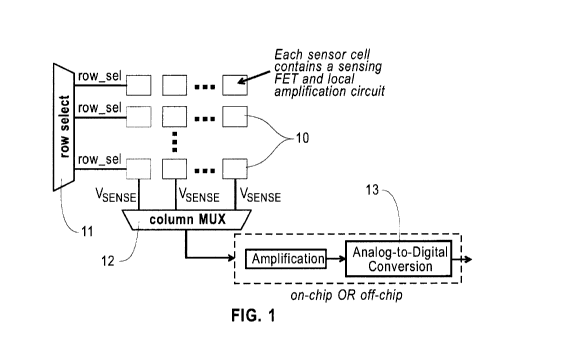
[0027] Reference may now be had to FIG. 1. FIG. 1 illustrates an exemplary
embodiment of an array of sensor cells 10. Each sensor cell 10 is configured
to sense a
biomolecule and provide a signal such as a voltage reading that can be used to
detect the
biomolecule. The array of sensor cells 10 in the embodiment of FIG. I is a
matrix arrangement
wherein each cell 10 is defined by a row number and a column number. In the
embodiment of
FIG. 1, a row select circuit I I is configured to select a row of cells 10 to
be read by energizing
each sensor cell 10 in the selected row. A column multiplexing circuit 12 is
configured to read a
signal from one cell 10 in each column. Thus, by selecting a row, each cell 10
within the row
will be read by the column multiplexing circuit 12.
4
CA 02786285 2012-06-29
WO 2011/082395 PCT/US2011/020007
[00281 Still referring to FIG. I, the amplified signal or voltage reading for
each cell 10 is
referred to as VSENSE. VSENSE. is sent to relatively long interconnect lines
to be transferred
outside of the array for further processing. VSENSE may be amplified again
outside of the sensor
cell 10 and then converted to a digital signal via an analog to digital
converter (ADC) 13. In one
embodiment, there can be as many ADCs as there are sensor cells 10 in a row,
so that all VSENSE
outputs from each row can be simultaneously converted to the digital signal.
In another
embodiment, there can be less ADCs. Using less ADCs requires selecting the
VSENSE signals in
an order using the column multiplexing circuit. This will take more time to
perform the analog
to digital conversion, but an advantage is that less area will be required on
a semiconductor chip.
[00291 Reference may now be had to FIG. 2. FIG. 2 illustrates an exemplary
embodiment of an FET 20 configured to sense a biomolecule 21. The FET 20 in
the
embodiment of FIG. I is a finFET having a fin 22 covered with a gate
dielectric 23. One non-
limiting embodiment of the gate dielectric 23 is Si02/HfO2. The gate
dielectric 23 is covered
with a gate surface material 24 that is configured to adhere to the
biomolecule 21. The FET 20
does not have a conventional top gate. An electrolyte 25 surrounds the gate
surface material 24
and acts as the top gate. The fin 22 and the gate dielectric 23 are situated
atop a buried oxide
(BOX) layer 26 that is situated atop of a silicon layer 27, which is the back
gate of the FET 20.
[0030] The drain current of the FET 20 is operated in the sub-threshold
region. To sense
the biomolecule 21, the biomolecule 21 binds to the gate surface material 24
and transfers an
electric charge to the gate dielectric 23. The electric charge at the gate
dielectric 23 affects the
drain current, which in turn affects the drain to source voltage of the FET
20. The measured
drain to source voltage is VSENSE. In that each different biomolecule 21
generally has a unique
electrical charge, the measurement of VSENSE can be used to identify the
specific biomolecule 21
being detected.
[00311 The advantage of using an FET 20 to sense the biomolecule 21 is that
the FET 20
has high sensitivity to the electric charge of the biomolecule 21. The high
sensitivity results
from a small sub-threshold slope such that a small change in the gate voltage
causes a large
change in the drain current resulting in a large change in the drain to source
voltage (i.e.,
VSENSE), The larger surface area of the gate dielectric 23 in finFETs compared
to non-fin FETs
CA 02786285 2012-06-29
WO 2011/082395 PCT/US2011/020007
results in an improved response time. The finFET used as the FET 20 can have a
single fin or an
array of fins to further increase the surface area of the gate dielectric 23.
100321 While the embodiment of FIG. 2 illustrates a finFET, other types of
FETs may
also be used to detect the biomolecule 21. The FET 20 is generally implemented
using
complementary metal-oxide-semiconductor (CMOS) technology.
[00331 Reference may now be had to FIG. 3. FIG. 3 illustrates a schematic
diagram of
an inverting gain amplifier circuit 30. The inverting gain amplifier circuit
30 includes the FET
20 as the sensor for sensing the biomolecule 21. In the embodiment of FIG. 3,
the FET 20 is an
n-type FET and is designated FET Ni. The FET NI is coupled in series with a p-
type FET, FET
Pl. That is, the drain of FET Ni is coupled to the drain of FET P1 and the
source of FET P1 is
coupled to a power supply designated VDDI and supplying voltage VDDI.
Together, the FET N I
and the FET P1 form the inverting gain amplifier circuit 30. In addition,
another n-type FET,
FET N2, transfers the output of the FET Ni, Vx, which is related to the
detected electric charge
of the biomolecule 21, to a VSENSE line 31. The voltage read at the VSENSE
line 31 is referred to
as VSENSE= In the embodiment of FIG. 3, the VSENSE line 31 is outside of the
sensor cell 10. The
FET N2 is configured to receive a "row select" signal (i.e., row sel) from the
row select circuit
1 1 such that when a gate of the FET N2 is energized (i.e., set to VDDI), then
the output voltage,
Vx, is coupled to the VSENSE line 31. When FET N2 is "ON", then VSENSE becomes
generally the
same as Vx.
[0034] Reference may now be had to FIG. 4. FIG. 4 depicts aspects of inverting
gain
characteristics of the inverting gain amplifier circuit 30. The output of the
amplifier circuit 30 is
graphed versus the gate voltage, VGN, of FET N 1. The sensing FET N I is
biased to operate in
the sub-threshold region, such that 0<VGN<VT,NI. The p-type FET P1 is biased
to operate such
that VGP < VDDI - VT,PI, where VT,PI is the threshold of the p-type FET P I.
If the gate voltage,
VGN, of FET NI increases, then the voltage, Vx, will decrease according to the
slope of the
operating region in the curve in FIG. 4. Similarly, if the gate voltage, VGN,
of FET NI decreases,
then the voltage, Vx, increases according to the slope of the operating region
in that curve.
Because of the high sensitivity of the FET Nl, a small change in VGN will
generally result in a
large change in Vx.
6
CA 02786285 2012-06-29
WO 2011/082395 PCT/US2011/020007
100351 Reference may now be had to FIG. 5. FIG. 5 depicts aspects of the
sensor cell 10
having a circuit configured to have low resistance in the components coupling
Vx to the VSENSE
line. In the circuit of FIG. 5, a p-type FET, FET N2, is disposed in parallel
to FET N2 such that
the gate of FET N2 is coupled to the complement of the row select signal. This
configuration
will transfer a wide range of values of Vx to the VSENSE line. However, it is
noted that this
configuration will also increase leakage in the sensor cells 10 that are not
selected for reading.
100361 In the unselected sensor cells 10, there is a current path between VDDI
and ground,
GND. This can result in power consumption by a sensor cell 10 even if the cell
10 is not
accessed for reading. Three examples of techniques to overcome this power
consumption are
disclosed herein as described with reference to FIGS. 6, 7 and 8.
100371 Reference may now be had to FIG. 6. FIG. 6 depicts aspects of a circuit
configured to turn off the FET P1 in the sensor cells 10 that are not selected
for reading. The
circuit in FIG. 3 includes a p-type FET, FET P8, disposed between VDDI and
gates of all PI
FETs in a row of the array. Further, n-type FET N9 and p-type FET P9 are
connected in parallel
such that their drains are tied together and connected to VGP and their
sources are connected to
the gate of all P 1 FETs in the row of the array. The gates of FET P8 and FET
N9 are connected
to the row enable signal "row_sel." The gate of FET P9 is connected to the
complement of the
"row_sel" signal. This circuit is common to all sensor cells 10 in a row. All
the sensor cells 10
in a row have a common VGP. In the sensor cells 10 that are unselected, the
row select will be
"0" and, hence, the FET P8 will be ON connecting gates of all P1 FETs in a row
to VDDI. Thus,
in all the unselected sensor cells 10, the FET PI will be turned OFF to stop
the current flowing in
the path VDDI to GND. In a selected row, FET P8 will be OFF and FET P9 and FET
N9 will be
ON so as to connect the gate of all P 1 FETs in the row to VGP.
[00381 Reference may now be had to FIG. 7. FIG. 7 depicts aspects of a circuit
having a
p-type FET, FET P3, disposed in series with the FET P1, i.e., between the
power supply VDDI
and the source of the FET P1. The FET P3 is turned OFF when a row is not
selected, i.e., when
the row select signal is low, thus, stopping the current flowing in the path
VDD1 to GND.
[00391 Reference may now be had to FIG. 8. FIG. 8 depicts aspects of a circuit
having
an n-type FET, FET N3, disposed in series with the FET N1, i.e., between the
source of the FET
7
CA 02786285 2012-06-29
WO 2011/082395 PCT/US2011/020007
N I and the ground, GND. The FET N3 is turned OFF when a row is not selected,
i.e., when the
row select signal is low, thus, stopping the current flowing in the path VDD1
to GND.
100401 With reference to FIG. 1, several sensor cells 10 may be connected to
the
common VSENSE line resulting in the VSENSE line being very long and, hence,
having a relatively
large resistance and capacitance. At any given time, only one selected sensor
cell 10 may have a
measurement transmitted to the VSENSE line while the FET N2 (shown in FIGS. 3,
5, 7 and 8) in
other unselected sensor cells 10 is OFF. Since the FET N I and the FET P 1 are
operating in the
sub-threshold region and not in deep saturation (which occurs when VGN = VDDI
and VGP = 0),
the electrical currents through the FET N I and the FET P 1 are very low.
Hence, charging and/or
discharging of a connection line connecting the Vx signal to the VSENSE line
through the FET N1
and the FET P 1 can contribute significant noise to the Vx signal. In
addition, the charging
and/or discharging can cause an increase in the amount of time it takes to
stabilize the Vx signal
transmitted to the VSFNSE line. In order to prevent the noise and decrease the
stabilization time,
an amplifying and decoupling circuit disposed in the connection line is
disclosed.
100411 Reference may now be had to FIG. 9. FIG. 9 depicts aspects of an
amplifying and
decoupling circuit 90 that decouples the Vx signal from the VSENSE line and
also linearly
amplifies the Vx signal in the range of AVON before the Vx signal is
transmitted to the VSENSE
line. The amplifying and decoupling circuit 90 includes n-type FETs, FET N4
and FET N5, and
p-type FETs, FET P4 and FET P5. FETs N4, N5, P4 and P5 are configured as shown
in FIG. 9
between (1) a node at the inverting gain amplifier circuit 30 providing the Vx
signal and (2) the
VSENSE line. It is noted that FET N4 and FET P4 are in an inverter
configuration with the Vx
signal as input and VsENSE as output. FET N5 and FET P5 are feedback
transistors. In another
embodiment, multiple gate FETs such as finFETS with independent backgate
control may be
used in lieu of the single gate FETs to make the amplifying and decoupling
circuit 90. FET N4
and FET N5 can be substituted with a single multiple gate FET with FET N5 as a
backgate.
Similarly, FET P4 and FET P5 can be substituted with a single multiple gate
FET with FET P5
as a backgate. As shown in FIG. 9, the amplifying and decoupling circuit 90 is
coupled to a
separate power supply VDD2 (having voltage VDD2) so as to achieve a desired
voltage range for
VSENSE=
8
CA 02786285 2012-06-29
WO 2011/082395 PCT/US2011/020007
100421 The inverting gain amplifier circuit 30 is based on the change in Vx
due to a
change in VGN. The change in Vx due to a change in VGN can be
deterministically correlated
when AVx / AVGN is a definite function in the given range of AVGN. As FET NI
and FET PI
form an inverting gain circuit, the gain is very high near the biasing point,
i.e., at the chosen
value of VGN as shown in FIG. 4. Amplification of VGN is beneficial but the
amplification can
limit the range if values of AVGN due to saturation of Vx for low or high
values of VGN. It is
preferable to have correlation between AVx and AVGN in the full range of
values of AVGN.
100431 Reference may now be had to FIG. 10. FIG. 10 illustrates plots of
VSENSE and Vx
versus VGN. It is noted that linearization circuitry results in a linear
correlation between VSENSE
and VGN for a wide range of OVEN from the biasing point. FIG. 10 also shows a
plot of VSENSE
with and without the feedback FETs N5 and P5. Without feedback, the output of
the inverting
gain amplifier circuit 30 has very high amplification, thereby, having the
potential for a large
change in VSENSE for a little change in VGN. Thus, VSENSE can saturate for a
large change in VGN.
This potential for saturation limits the region of operation of VGN, hence,
feedback is necessary
for detecting the large change in VGN, due to detecting a large change in
electric charge of the
biomolecule 21.
100441 To reduce power consumption in the amplifier and decoupling circuit 90,
the
electric current path between power supply VDD2 and GND as shown in FIG. 9 can
be
interrupted. FIG. 11 depicts an embodiment for interrupting the current path
by disposing a p-
type FET, FET P6, between the power supply VDD2 and the sources of FETs P4 and
P5. FIG. 12
depicts another embodiment for interrupting the current path by disposing an n-
type FET, FET
N6, between the sources of FETs N4 and N5 and ground.
100451 The amplifying and decoupling circuit 90, which may include the current
interrupting circuitry, can be implemented in each sensor cell 10 or,
alternatively, by sharing the
circuit 90 with the sensor cells 10 in a column. In the sharing embodiment,
the amplifying and
decoupling circuit 90 is coupled between the VSENSE line and the column
multiplexing circuit 12
shown in FIG. Ito reduce the area needed by each sensor cell 10.
9
CA 02786285 2012-06-29
WO 2011/082395 PCT/US2011/020007
[00461 Sensor calibration to mitigate fabrication related variations is
discussed next. Due
to fabrication imperfections in a semiconductor chip used to fabricate the
array of sensor cells
10, FETs in the bio-sensing cell 10 may not have desired gate length, width,
threshold voltage
etc. Hence, pre-fabrication calibration of VSENSE to AVGN may not be accurate.
Therefore, post-
fabrication calibration of each sensor cell 10 is disclosed. Post-fabrication
can be achieved in the
following way. First, select a VGN based on pre-fabrication analysis. Second,
in the fabricated
chip, apply VGN and measure the VSFNSE (called VOSENSE) for each sensor cell
10. It is noted that
the biomolecule 21 is not present for this calibration measurement. VOSENSE is
the analog voltage
signal that is converted to a digital signal, which can be stored in a
conventional semiconductor
memory integrated onto the chip or connected externally. The stored digital
value of VOSENSE for
each sensor cell 10 will serve as reference point for future measurements
performed by that
sensor cell 10. Third, during a real sensing application, the measured digital
value of VSENSE will
be in reference to original stored value of VOSENSE. This calibration
technique does not require
any changes in the hardware. Hence, the same hardware can be repeatedly used
for different
kinds of biomolecules 21 after quick calibration i.e., measurement of VOSENSE.
[00471 Sensor tuning to test a variety of the biomolecules 21 that may require
different
biasing points (VGN) is discussed next. The range of operation of the sensing
FET NI depends
on the choice of biasing point VGN. The biological molecule 21 should not
experience any
resistance due to VGN while binding to the gate of the FET N1. If different
biomolecules 21
require different biasing points, i.e., VGN values, then the similar AVGN
values can be
determined. This can be achieved by dynamically controlling the threshold
voltage VT of FETs
Ni and P1. FIG. 13 illustrates the movement of biasing point VGN with the
change in VT of
FETs N I and P l. This AVT, N 1, Pi can be achieved by changing the substrate
bias of FETs N 1 and
PI (i.e., single gate FETs) with substrate contact. In multiple-gate FETs such
as finFETs, VT can
be dynamically modified by controlling the voltage bias at the back (or
second) gate of these
FETs.
100481 FIG. 14 presents one example of a method 140 for identifying the
biomolecule 21
having an associated electric charge. The method 140 calls for (step 141)
sensing the electric
charge of the biomolecule 21 with the gate dielectric 23 of the FET 20. The
FET 20 and another
FET are configured to form the inverting gain amplifier circuit 30. Further,
the method 140 calls
CA 02786285 2012-06-29
WO 2011/082395 PCT/US2011/020007
for (step 142) measuring the electric charge at the gate with the inverting
gain amplifier circuit to
identify the biomolecule 21.
[00491 While the method 140 and the discussion presented above are with
respect to
identifying the biomolecule 21, any material having an electric charge that
may adhere to the
gate dielectric 23 can be identified. In general, testing and/or analysis of
different biomolecules
21 and materials having differing electric charges are used to determine a
reference electric
charge associated with each test biomolecule 21/material. Thus, by comparing
the measured
electric charge with reference electric charges, the biomolecule 21/material
can be identified.
100501 In one embodiment, the array of sensors 10 can be built into one CMOS
device or
semiconductor "chip" to lower production cost and improve reliability. In
addition, other
components used with the array of sensors 10, such as the row select circuit
11, the column
multiplexing circuit 12 and the ADC 13, can also be built into the same CMOS
device.
[00511 The capabilities of the present invention can be implemented in
software,
firmware, hardware or some combination thereof.
100521 As one example, one or more aspects of the present invention can be
included in
an article of manufacture (e.g., one or more computer program products)
having, for instance,
computer usable media. The media has embodied therein, for instance, computer
readable
program code means for providing and facilitating the capabilities of the
present invention. The
article of manufacture can be included as a part of a computer system or sold
separately.
100531 Additionally, at least one program storage device readable by a
machine, tangibly
embodying at least one program of instructions executable by the machine to
perform the
capabilities of the present invention can be provided.
100541 In support of the teachings herein, various analysis components may be
used,
including a digital and/or an analog system. The system may have components
such as a
processor, storage media, memory, input, output, communications link, user
interfaces (such as a
printer or a display), software programs, signal processors (digital or
analog) and other such
components (such as resistors, capacitors, inductors and others) to provide
for operation and
11
CA 02786285 2012-06-29
WO 2011/082395 PCT/US2011/020007
analyses of the apparatus and methods disclosed herein in any of several
manners well-
appreciated in the art. It is considered that these teachings may be, but need
not be, implemented
in conjunction with a set of computer executable instructions stored on a
computer readable
medium, including memory (ROMs, RAMs), optical (CD-ROMs), or magnetic (disks,
hard
drives), or any other type that when executed causes a computer to implement
the method of the
present invention. These instructions may provide for equipment operation,
control, data
collection and analysis and other functions deemed relevant by a system
designer, owner, user or
other such personnel, in addition to the functions described in this
disclosure.
[0055] The flow diagrams depicted herein are just examples. There may be many
variations to these diagrams or the steps (or operations) described therein
without departing from
the spirit of the invention. For instance, the steps may be performed in a
differing order, or steps
may be added, deleted or modified. All of these variations are considered a
part of the claimed
invention.
[0056] Elements of the embodiments have been introduced with either the
articles "a" or
"an." The articles are intended to mean that there are one or more of the
elements. The terms
"including" and "having" are intended to be inclusive such that there may be
additional elements
other than the elements listed. The conjunction "or" when used with a list of
at least two terms is
intended to mean any term or combination of terms. The terms "first,"
"second," "third," etc. are
used to distinguish elements and are not used to denote a particular order.
The term "couple"
relates to one component being coupled either directly to another component or
indirectly to the
another component via one or more intermediate components.
[0057] While the invention has been described with reference to a preferred
embodiment
or embodiments, it will be understood by those skilled in the art that various
changes may be
made and equivalents may be substituted for elements thereof without departing
from the scope
of the invention. In addition, many modifications may be made to adapt a
particular situation or
material to the teachings of the invention without departing from the
essential scope thereof.
Therefore, it is intended that the invention not be limited to the particular
embodiment disclosed
as the best mode contemplated for carrying out this invention, but that the
invention will include
all embodiments falling within the scope of the appended claims.
12