Note: Descriptions are shown in the official language in which they were submitted.
CA 02786462 2012-07-04
WO 2011/085048 PCT/US2011/020286
IMPROVED POWER SUPPLY AND METHOD RELATED THERETO
CROSS-REFERENCE TO RELATED APPLICATIONS
[0001] This application claims the benefit of. (1) U.S. Provisional
Application Ser. No. 61/292,490, filed on January 5, 2010; (2) PCT
Application No. PCT/US2009/041476, filed April 22, 2009; and (3) U.S.
Non-Provisional Application Ser. No. 12/428,468, filed on April 22, 2009.
PCT Application No. PCT/US2009/041476 and U.S. Non-Provisional
Application Ser. No. 12/428,468 both claim the benefit of: (1) U.S.
Provisional Application Ser. No. 61/155,468, filed on February 25, 2009;
and (2) U.S. Provisional Application Ser. No. 61/047,070, filed on April
22, 2008.
TECHNICAL FIELD
[0002] Subject matter described herein relates to power supply devices,
and more particularly to the internal power management of power supplies
for electronic devices.
BACKGROUND
[0003] Electronic devices of all types have become more and more
common in everyday life. Electronic devices include non-portable devices
as well as portable devices. Examples of non-portable electronic devices
include wired telephones, routers (wired and wireless), wireless access
points (WAPs) and the like. Examples of portable electronic devices
include cellular phones, personal data assistants (PDAs), combination
cellular phone and PDAs (e.g., a Blackberry device available from
Research in Motion (RIM ) of Ontario, Canada), cellular phone
accessories (e.g., a Bluetooth enabled wireless headset), MP3 (Moving
Pictures Experts Group-1 Audio Layer 3) players (e.g., an iPod device
by Apple Inc. (Apple ) of Cupertino, CA), compact disc (CD) players,
and digital video disk (DVD) players. Along with the positive benefits of
use of such devices comes the requirement to power the devices and/or
communicate with them. Power supplies use power even when not
supplying power to electronic devices that are in electrical communication
CA 02786462 2012-07-04
WO 2011/085048 PCT/US2011/020286
with the power supplies. Reducing the administrative power consumption
of the power supplies for such devices can prove difficult.
BRIEF DESCRIPTION OF THE DRAWINGS
[0004] To facilitate further description of the embodiments, the following
drawings are provided in which:
[0005] FIG. 1 is a block diagram illustrating an improved power supply
including aspects of the subject matter described herein;
[0006] FIG. 2 is a block diagram illustrating an embodiment of the
improved power supply of Figure 1 including aspects of the subject matter
described herein;
[0007] FIG. 3 is a block diagram illustrating another embodiment of the
improved power supply of Figure 1 including aspects of the subject matter
described herein;
[0008] FIG. 4 is a block diagram illustrating yet another embodiment of the
improved power supply of Figure 1 including aspects of the subject matter
described herein;
[0009] FIG. 5 is a schematic diagram illustrating an embodiment of a metal
oxide varistor (MOV) protection circuit portion of Figures 2 - 4 including
aspects of the subject matter described herein;
[0010] FIG. 6 is a schematic diagram illustrating an embodiment of the
improved power supply of Figure 2 that includes aspects of the subject
matter described herein;
[0011] FIG. 7 is a schematic diagram illustrating an embodiment of the
improved power supply of Figure 3 that includes aspects of the subject
matter described herein;
[0012] FIG. 8 is a schematic diagram illustrating an embodiment of the
improved power supply of Figure 4 that includes aspects of the subject
matter described herein;
2
CA 02786462 2012-07-04
WO 2011/085048 PCT/US2011/020286
[0013] FIG. 9 is a schematic diagram illustrating another embodiment of the
improved power supply of Figure 2 that includes aspects of the subject
matter described herein;
[0014] FIG. 10 is block diagram illustrating a method for providing
improved power that includes aspects of the subject matter described
herein;
[0015] FIG. 11 is an isometric view of an embodiment of a housing for an
improved power supply;
[0016] FIG. 12 is a block diagram illustrating another embodiment of an
improved power supply;
[0017] FIG. 13 is an embodiment of a schematic diagram of the improved
power supply of FIG. 12; and
[0018] FIGs. 14-17 are additional isometric views of the embodiment of the
housing for the improved power supply of FIG. 11.
[0019] The phrase "subject matter described herein" refers to subject matter
described in the Detailed Description unless the context clearly indicates
otherwise. The term "aspects" is to be read as "at least one aspect."
Identifying aspects of the subject matter described in the Detailed
Description is not intended to identify key or essential features of the
claimed subject matter. The aspects described above and other aspects of
the subject matter described herein are illustrated by way of example and
not limited in the accompanying figures in which like reference numerals
indicate substantially similar elements.
[0020] For simplicity and clarity of illustration, the drawing figures
illustrate the general manner of construction, and descriptions and details
of well-known features and techniques may be omitted to avoid
unnecessarily obscuring aspects of the subject matter described herein.
Additionally, elements in the drawing figures are not necessarily drawn to
scale. For example, the dimensions of some of the elements in the figures
may be exaggerated relative to other elements to help improve
understanding of embodiments of the subject matter described herein.
3
CA 02786462 2012-07-04
WO 2011/085048 PCT/US2011/020286
[0021] The terms "first," "second," "third," "fourth," and the like in the
Detailed Description and in the claims, if any, are used for distinguishing
between similar elements and not necessarily for describing a particular
sequential or chronological order. It is to be understood that the terms so
used are interchangeable under appropriate circumstances such that the
embodiments of the subject matter described herein are, for example,
capable of operation in sequences other than those illustrated or otherwise
described herein. Furthermore, the terms "include," and "have," and any
variations thereof, are intended to cover a non-exclusive inclusion, such
that a process, method, system, article, or apparatus that comprises a list of
elements is not necessarily limited to those elements, but may include
other elements not expressly listed or inherent to such process, method,
article, or apparatus.
[0022] The terms "left," "right," "front," "back," "top," "bottom," "over,"
"under," and the like in the Detailed Description and in the claims, if any,
are used for descriptive purposes and not necessarily for describing
permanent relative positions. It is to be understood that the terms so used
are interchangeable under appropriate circumstances such that the aspects
of the subject matter described herein are, for example, capable of
operation in other orientations than those illustrated or otherwise described
herein. The term "on," as used herein, is defined as on, at, or otherwise
substantially adjacent to or next to or over.
[0023] The terms "couple," "coupled," "couples," "coupling," and the like
should be broadly understood and refer to connecting two or more
elements or signals, electrically, mechanically, or otherwise, either directly
or indirectly through intervening circuitry and/or elements. Two or more
electrical elements may be electrically coupled, either direct or indirectly,
but not be mechanically coupled; two or more mechanical elements may
be mechanically coupled, either direct or indirectly, but not be electrically
coupled; two or more electrical elements may be mechanically coupled,
directly or indirectly, but not be electrically coupled. Coupling (whether
4
CA 02786462 2012-07-04
WO 2011/085048 PCT/US2011/020286
only mechanical, only electrical, both, or otherwise) may be for any length
of time, e.g., permanent or semi-permanent or only for an instant.
[0024] "Electrical coupling" and the like should be broadly understood and
include coupling involving any electrical signal, whether a power signal, a
data signal, and/or other types or combinations of electrical signals.
"Mechanical coupling" and the like should be broadly understood and
include mechanical coupling of all types.
[0025] The absence of the word "removably," "removable," and the like
near the word "coupled," and the like does not mean that the coupling, etc.
in question is or is not removable. For example, the recitation of a clip
being coupled to an outer casing does not mean that the clip cannot be
removed (readily or otherwise) from, or that it is permanently connected
to, the outer casing.
DETAILED DESCRIPTION OF EXAMPLES OF EMBODIMENTS
[0026] Some embodiments include an electrical system. In many
embodiments, the electrical system can comprise a power input. In the
same or different embodiments, the electrical system can comprise at least
one power output configured to be electrically coupled to at least one load.
In the same or different embodiments, the electrical system can comprise a
first user input device configured to provide a start up input. In the same
or different embodiments, the electrical system can comprise a second
user input device configured to provide a time select input. In the same or
different embodiments, the electrical system can comprise an internal
assembly. In many embodiments, the internal assembly can comprise a
power switch module electrically coupled between the power input and the
at least one power output. In various embodiments, the power switch
module can be configured to receive a first power signal from the power
input. In the same or different embodiments, the power switch module
can comprise a control mechanism configured to open and close to
regulate a flow of the first power signal to the at least one power output.
In many embodiments, the internal assembly can comprise a power
CA 02786462 2012-07-04
WO 2011/085048 PCT/US2011/020286
conserve module electrically coupled to the power switch module. In
various embodiments, the power conserve module can be configured to
receive the first power signal from the power switch module, to receive
the start up input from the first user input device, and to attenuate the
first
power signal to a second power signal and a third power signal at different
times. In many embodiments, the internal assembly can comprise a power
supply module electrically coupled between the power switch module and
the power conserve module. In the same or different embodiments, the
power supply module can be configured to receive the second power
signal and the third power signal at different times from the power
conserve module, to convert the second power signal into a fourth power
signal and a fifth power signal at different times, to convert the third
power signal into a sixth power signal and a seventh power signal at
different times, and to provide the fourth power signal and the sixth power
signal at different times to the power switch module. In many
embodiments, the internal assembly can comprise a control module
electrically coupled between the power supply module and the power
switch module. In the same or different embodiments, the control module
can be configured to receive the fifth power signal and the seventh power
signal at different times from the power supply module and to receive the
time select input from the second user input device.
[0027] Further embodiments can include a method for manufacturing an
electrical system. In many embodiments, the method can comprise:
providing a power input; providing at least one power output configured to
be electrically coupled to at least one load; providing a first user input
device configured to provide a start up input; providing a second user
input device configured to provide a time select input; providing an
internal assembly comprising, where the internal assembly comprises a
power switch module configured to receive a first power signal from the
power input and comprising a control mechanism that opens and closes to
regulate a flow of the first power signal to the at least one power output, a
6
CA 02786462 2012-07-04
WO 2011/085048 PCT/US2011/020286
power conserve module configured to receive the first power signal, to
receive the start up input, and to attenuate the first power signal to a
second power signal and a third power signal, a power supply module
configured to receive the second power signal and the third power signal,
to convert the second power signal into a fourth power signal and a fifth
power signal, to convert the third power signal into a sixth power signal
and a seventh power signal, and to provide the fourth power signal and the
sixth power signal to the power switch module, and a control module
configured to receive the fifth power signal, the seventh power signal, and
the time select input; coupling the power input to the power switch
module; coupling the at least one power output to the power switch
module; coupling the power switch module to the power conserve module;
coupling the power switch module to the power supply module; coupling
the power conserve module to the power supply module; coupling the
power supply module to the control module; and coupling the control
module to the power switch module.
[0028] Other embodiments can include a method for regulating a flow of a
first power signal to at least one power output attenuating the first power
signal to a second power signal having a lower voltage than the first power
signal. In the same or different embodiments, the method can comprise:
converting the second power signal to a third power signal and a fourth
power signal, the second power signal having an alternating current and
the third power signal and fourth power signal having direct currents;
permitting the first power signal to flow to the at least one power output
after receiving a control mechanism activation signal; activating a
countdown register such that the countdown register counts down from a
time interval until the time interval elapses; attenuating the first power
signal to a fifth power signal having a lower voltage than the first power
signal and the second power signal; converting the fifth power signal to a
sixth power signal and a seventh power signal, the fifth power signal
having an alternating current and the sixth power signal and the seventh
7
CA 02786462 2012-07-04
WO 2011/085048 PCT/US2011/020286
power signal having direct currents; powering the control mechanism with
the sixth power signal such that the control mechanism remains in a state
permitting the first power signal to flow to the at least one power output;
referencing the countdown register to determine whether the time interval
has elapsed; prohibiting the first power signal from flowing to the at least
one power output when the time interval elapses or after the time interval;
and prohibiting the flow of the first power signal to the at least one power
output such that approximately zero power passes to the at least one power
output when the countdown register is not counting down from the time
interval.
[0029] In some examples, a relocatable power tap can be configured to
removably couple to an external device. The relocatable power tap can
include: (a) at least one controlled power outlet; (b) a power supply circuit
configured to receive an input AC power signal and produce an output AC
power signal, the power supply circuit having a first stage and a second
stage, the first stage of the power supply circuit configured to produce a
first DC power signal and the second stage of the power supply circuit
configured to produce a second DC power signal; (c) a control circuit in
electrical communication with the power supply circuit and configured to
receive the output AC power signal, the first DC power signal, and the
second DC power signal, the control circuit can include: (1) a driver
circuit, the driver circuit configured to receive the second DC power signal
as a power source, the driver circuit further configured to receive a
command signal and produce a control signal based on the command
signal; and (2) a controlled switching circuit in electrical communication
with the driver circuit and configured to receive the first DC power signal
as a power source and to receive the output AC power signal, the
controlled switching circuit further configured to receive the control signal
from the driver circuit and provide the output AC power signal to the at
least one controlled power outlet based on the control signal; and (d) an
input circuit, the input circuit coupled to the control circuit and configured
8
CA 02786462 2012-07-04
WO 2011/085048 PCT/US2011/020286
to provide the command signal to the driver circuit of the control circuit,
the command signal indicating whether the at least one controlled power
outlet is to receive the output AC power signal. The at least one
controlled power outlet can have an input electrically coupled to the
controlled switching circuit and an output configured to electrically
coupled to the external device, the at least one controlled power outlet
configured to receive the output AC power signal from the controlled
switching circuit and provide the output AC power signal to the external
device.
[0030] In the same or different embodiment, a power supply for a
relocatable power tap can be configured to couple to an external load. The
power supply can include: (a) a first power supply module configured to
receive an input AC power signal; and (b) a second power supply module
coupled to the first power supply module. The first power supply module
and the second power supply module can be configured to provide an
output AC power signal to the external load, a first DC power signal to a
first internal load, and a second DC power signal to a second internal load.
[0031] In some examples, the first power supply module can include a
reactive voltage divider circuit, a rectifier circuit, and a shunt regulator
circuit. The first power supply module can be configured to receive the
input AC power signal and produce the first DC power signal. The first
DC power signal can have at least a first state and a second state. An
amplitude of a voltage associate with the first state of the first DC power
signal can be sufficient to activate the first internal load. An amplitude of
a voltage associated with the second state of the first DC power signal can
be sufficient to maintain activation of the first internal load. The second
power supply module can include a voltage regulator circuit. The second
power supply module can be configured to receive the first DC power
signal and produce the second DC power signal.
[0032] In many examples, the first power supply module can include a
reactive voltage divider circuit, a rectifier circuit, and a shunt regulator
9
CA 02786462 2012-07-04
WO 2011/085048 PCT/US2011/020286
circuit. The first power supply module can be configured to receive the
input AC power signal and produce the first DC power signal. The first
DC power signal can have at least a first state and a second state. An
amplitude of a voltage associate with the first state of the first DC power
signal can be sufficient to activate the first internal load. An amplitude of
a voltage associated with the second state of the first DC power signal can
be sufficient to maintain activation of the first internal load. The second
power supply module can include a reactive voltage divider circuit, a
rectifier circuit, and a voltage regulator circuit. The second power supply
module can be configured to receive the first DC power signal and
produce the second DC power signal.
[0033] In various embodiments, the power supply can further include a
transformer having at least a primary winding and two or more secondary
windings. The transformer can be configured to receive the input AC
power signal and produce at least a first AC power signal and a second AC
power signal. The first power supply module can be reactively coupled
and in electrical communication with a first secondary winding of the two
or more secondary windings. The first power supply module can include a
rectifier circuit and an energy storage circuit. The first power supply
module can be configured to receive the first AC power signal and
produce the first DC power signal. The first DC power signal can have at
least a first state and a second state. An amplitude of a voltage associate
with the first state of the first DC power signal can be sufficient to
activate
the first internal load. An amplitude of a voltage associate with the second
state of the first DC power signal can be sufficient to maintain activation
of the first internal load. The second power supply module can be in
electrical communication with a second secondary winding of the two or
more secondary windings. The second power supply module can include
a rectifier circuit and a voltage regulator circuit. The second power supply
module can be configured to receive the second AC power signal and
produce the second DC power signal.
CA 02786462 2012-07-04
WO 2011/085048 PCT/US2011/020286
[0034] In the same or different examples, the first internal load can be a
switch circuit coupled to the first power supply module and the second
power supply module. The switch circuit can be operable to provide the
output AC power signal to the external load when activated by the first
DC power signal.
[0035] In many examples, the second internal load is a control circuit
coupled to the second power supply module, and the switch circuit. The
control circuit can be operable to control the switch circuit when powered
by the first DC power signal. The switch circuit can be selected from the
group consisting of. an electro-mechanical switch circuit, a solid-state
switch circuit, or a vacuum tube switch circuit. The second internal load
can be a control circuit coupled to the second power supply module, and
the switch circuit; and the control circuit is operable to control the switch
circuit when powered by the first DC power signal. The external load is
configured as one or more controlled power outlets.
[0036] Still other embodiments disclose a method for providing an output
AC power signal. The method can include: producing an output AC
power signal, a first DC power signal, and a second DC power signal at a
power supply and based on a received input AC power signal; producing a
control signal at a control circuit at least in part based the second DC
power signal; powering a switch circuit with the first DC power signal
based on the control signal and the second DC power signal; and
providing the output AC power signal to a load when the switch circuit is
powered.
[0037] In still further embodiments an apparatus can include: (a) a power
supply having: (1) a first power supply module configured to receive a
first input power signal and further configured to provide a first DC output
power signal at a first power level; and (2) a second power supply module
electrically coupled to the first power supply module and configured to
provide a second DC output power signal at a second power level, the
second power level is lower than the first power level; (b) a first circuit
11
CA 02786462 2012-07-04
WO 2011/085048 PCT/US2011/020286
receiving the first DC output power signal; and (c) a second circuit
receiving the second DC output power signal. In some examples, the
second power supply module is electrically coupled in series with the first
power supply module such that the second power supply module receives
the first DC output power signal as a second input power signal. In other
examples, the second power supply module is electrically coupled in
parallel with the first power supply module such that the second power
supply module receives the first input power signal.
[0038] In additional embodiments,
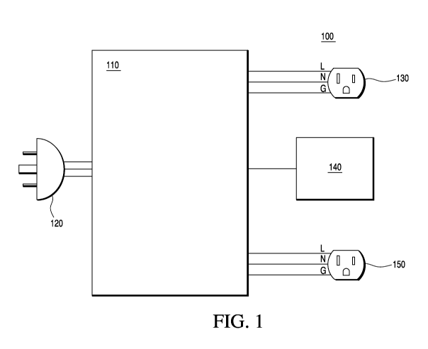
[0039] Figure 1 is a block diagram illustrating an embodiment of an
exemplary system for providing a multi-outlet controlled power strip
including multiple inputs, surge protection and incorporating an improved
power supply. Figure 1 includes power strip 100 (also called a relocatable
power tap (RPT)) including control circuitry 110, power plug 120,
constant "on" outlet(s) 130, command input device 140 and controlled
outlet(s) 150. Control circuitry 110 is a circuit configured to receive
power signals and disperse power signals to constant "on" outlet(s) 130
and possibly command input device 140 if so configured, and further
disperse power signals to controlled outlet(s) 150 based on input received
from command input device 140. Control circuitry 110 can include some
or all the improved power supply circuitry that is detailed in Figures 2 - 4
as well as in Figures 6 - 8 below. In some embodiments, control circuitry
110 additionally includes protection circuitry. Protection circuitry is
described in Figure 2 and specifically detailed in Figure 5, below.
[0040] Power plug 120 is an electrical conduit that is physically coupled to
and in electrical communication with control circuitry 110. Power plug
120 is configured to pass a power signal received from a power source to
control circuitry 110 when power plug 120 is physically coupled to and in
electrical communication with a power source (not shown). Constant "on"
outlet(s) 130 are a power outlet that are physically coupled to and in
constant electrical communication with control circuitry 110 and are
12
CA 02786462 2012-07-04
WO 2011/085048 PCT/US2011/020286
further configured to pass a power signal received from control circuitry
110 to any device with which it is in electrical communication.
[0041] Command input device 140 is any input device that is physically
coupled to and in electrical communication with control circuitry 110 and
is further configured to pass a command signal to control circuitry 110
based on a received command signal or command action that command
input device 140 received previously. Controlled outlet(s) 150 are a
power outlet that are physically coupled to and in controlled electrical
communication with control circuitry 110 and are further selectively
configured to pass a power signal received from control circuitry 110 to
any device with which it is in electrical communication. Command input
device 140 can be implemented as any suitable command input device,
such as, for example a master outlet as part of a master/slave power strip
configuration providing a control signal to control circuitry 110 by
drawing current from control circuitry 110, a receiver device providing a
control signal to control circuitry 110, a sensing device providing a control
signal to control circuitry 110, and the like. Examples of a receiver device
providing a control signal to control circuitry 110 include a radio
frequency (RF) receiver, a light emitting diode (LED) receiver, a wireless
networked receiver, a short range wireless receiver that is part of a
personal area network (PAN), and the like.
[0042] In operation, when power plug 120 is operably coupled to and in
electrical communication with an appropriate power source (e.g., an
alternating current (a.c.) or other power outlet fixture), power becomes
available to constant "on" outlet(s) 130 and command input device 140, as
appropriate. At this time, if command input device 140 has not provided
an appropriate command signal to control circuitry 110, power is NOT
available to controlled outlet(s) 150, and any device(s) operably coupled
to and in electrical communication with controlled outlet(s) 150 will NOT
receive any current or power. Control circuitry 110 is configured to detect
when a control signal is received from command input device 140. In an
13
CA 02786462 2012-07-04
WO 2011/085048 PCT/US2011/020286
example, when command input device 140 provides an "on" control signal
to control circuitry 110, control circuitry 110 will provide power to
controlled outlet(s) 150 thereby providing current and/or power to any
devices coupled to and in electrical communication with controlled
outlet(s) 150. Similarly, when command input device 140 provides an
"off' control signal to control circuitry 110 and then changes the control
signal to an "on" control signal, control circuitry 110 will provide power
to controlled outlet(s) 150 thereby providing current and/or power to any
devices coupled to and in electrical communication with controlled
outlet(s) 150.
[0043] The exemplary configuration illustrated in Figure 1 allows a user, via
constant "on" outlet(s) 130, the flexibility to assign certain devices (e.g.,
a
clock, cable/satellite receiver, etc.) to be supplied with constant power as
well as determine when other devices receive power. Additionally, the
configuration allows a user, via command input device 140 and controlled
outlet(s) 150, to control when power is supplied to a primary device (e.g.,
a personal computer, such as, a laptop or desktop computer) as well as or
in addition to secondary devices, such as, peripherals (e.g., printers,
scanners, etc.).
[0044] Figure 2 is a block diagram illustrating an embodiment of an
exemplary system for providing a multi-outlet controlled power strip
including surge protection and incorporating an improved power supply.
The power strip 200 in Figure 2 is a detailed view of power strip 100 of
Figure 1. As shown in Figure 2, power strip 200 includes: control
circuitry 110, power plug 120, constant "on" outlet(s) 130, command input
device 140 (configured as a master outlet) and controlled outlet(s) 150.
Control circuitry 110 includes metal oxide varistors (MOV) protection
circuit 260, hi-power (HI PWR) circuit 270, low-power (LO PWR) circuit
280 and control circuit 290. Command input device 140 includes master
outlet 240, sensing (SENSE) circuit 242 amplification (AMP) circuit 244.
14
CA 02786462 2012-07-04
WO 2011/085048 PCT/US2011/020286
Elements numbered as in Figure 1 function in a substantially similarly
way.
[0045] MOV protection circuit 260 has an input and an output. The input of
MOV protection circuit 260 is electrically coupled and in communication
with power plug 120. The output of MOV protection circuit 260 is
electrically coupled and in communication with constant "on" outlet(s)
130, master outlet 240 portion of command input device 140, HI PWR
circuit 270, LO PWR circuit 280, and control circuit 290. MOV
protection circuit 260 receives a power signal from power plug 120 and
provides protected power signals to constant "on" outlet(s) 130, command
input device 140, HI PWR circuit 270, LO PWR circuit 280, and control
circuit 290. An embodiment of MOV protection circuit 260 is described
in Figure 5, below. In operation, MOV protection circuit 260 provides
one or more of the following: conditions the received power signal to,
among other things, reduce incoming radiated and conducted high
frequency signals and noise; reduces the amplitude of incoming
overvoltage spikes/surges; provides protection for power strip 200 from
defective MOV units within MOV protection circuit 260; and determines
the presence of a ground connection as well as communicate that
information to a user. In short, MOV protection circuit 260 provides
protected power to all other circuitry and outlets within power strip 200.
[0046] HI PWR circuit 270 has an input and an output. The input of HI
PWR circuit 270 is electrically coupled and in communication with MOV
protection circuit 260, constant "on" outlet(s) 130, master outlet 240
portion of command input device 140 and LO PWR circuit 280. The
output of HI PWR circuit 270 is electrically coupled and in
communication with control circuit 290. LO PWR circuit 280 has an
input and an output. The input of LO PWR circuit 280 is electrically
coupled and in communication with MOV protection circuit 260, constant
"on" outlet(s) 130, master outlet 240 portion of command input device 140
and HI PWR circuit 270. The output of LO PWR circuit 280 is
CA 02786462 2012-07-04
WO 2011/085048 PCT/US2011/020286
electrically coupled and in communication with AMP circuit 244 portion
of command input device 140. HI PWR circuit 270 and LO PWR circuit
280 each receive a protected alternating current (AC) power signal from
MOV protection circuit 260 and generate different levels of low voltage
power for the internal circuitry of power strip 200. HI PWR circuit 270
and LO PWR circuit 280 efficiently convert line AC power to the voltages
required to operate control circuit 290 and AMP circuit 244, respectively.
HI PWR circuit 270 and LO PWR circuit 280 can be optimized to take
advantage of the most efficient power levels to run the internal circuitry of
power strip 200. In operation, LO PWR circuit 280 supplies real power to
AMP circuit 244, and HI PWR circuit 270 supplies real power to the
control circuit 290 allowing for efficient use of power. The uniqueness of
this approach as compared to a more traditional single power supply
approach is that a power savings as high as 4 to 1 can be achieved over the
traditional method. An embodiment of HI PWR circuit 270 and LO PWR
circuit 280 and the advantages of utilizing this configuration are further
described in Figures 6 - 8, below.
[0047] Control circuit 290 has an input and an output. The input of
control circuit 290 is electrically coupled and in separate communication
with MOV protection circuit 260, HI PWR circuit 270 and AMP circuit
244 portion of command input device 140. The output of control circuit
290 is electrically coupled and in communication with controlled outlet(s)
150. Control circuit 290 receives a real power signal from HI PWR circuit
270 and additionally receives a driving signal from AMP circuit 244 when
a device that is plugged into master outlet 240 portion of command input
device 140 is drawing enough power to be active. When control circuit
290 receives the driving signal from AMP circuit 244, control circuit 290
allows current to flow between MOV protection circuit 260 and controlled
outlet(s) 150.
[0048] SENSE circuit 242 of command input device 140 includes an input
and an output. The input of SENSE circuit 242 is electrically coupled and
16
CA 02786462 2012-07-04
WO 2011/085048 PCT/US2011/020286
in communication with master outlet 240 of command input device 140.
The output of SENSE circuit 242 is electrically coupled and in
communication with AMP circuit 244 of command input device 140.
SENSE circuit 242 monitors an output signal from master outlet 240 and
provides a sensing signal to AMP circuit 244 indicating whether or not
master outlet 240 is in use or is at least drawing current above a threshold
or minimum predetermined valve. In operation, SENSE circuit 242
determines that master outlet 240 is drawing current when a device that is
in electrical communication with master outlet 240 is drawing enough
current to exceed a current threshold, such as drawing enough current to
power the device in an "ON" state. In such a situation, SENSE circuit 242
produces a sensing signal in response to master outlet 240 drawing at least
a predetermined amount of current and provides the created sensing signal
to AMP circuit 244. In some embodiments, SENSE circuit 242 is
powered by master outlet 240 because master outlet 240 is always "ON."
In such embodiments, current drawn from master outlet 240 that is
monitored by SENSE circuit 242 can exclude the current (and power) that
SENSE circuit 242 requires to run, and/or SENSE circuit 242 can be
programmed (by hardware, software, or otherwise) or adjusted to account
for the current (and power) that SENSE circuit 242 draws from master
outlet 240.
[0049] AMP circuit 244 of command input device 140 includes an input
and an output. The input of AMP circuit 244 is electrically coupled and in
separate communication with SENSE circuit 242 and LO PWR circuit
280. The output of AMP circuit 244 is electrically coupled and in
communication with control circuit 290. AMP circuit 244 receives a real
power signal from LO PWR circuit 280 and additionally receives a
sensing signal from SENSE circuit 242 that is based on the status of
master outlet 240. AMP circuit 244 compares the signal received from
SENSE circuit 242 to a threshold to determine whether master outlet 240
is "on." If the signal received from SENSE circuit 242 equals or exceeds
17
CA 02786462 2012-07-04
WO 2011/085048 PCT/US2011/020286
a threshold value, AMP circuit 244 generates a driving signal and provides
the generated driving signal to control circuit 290.
[0050] In operation, power strip 200 enables a user to configure the power
strip to utilize one primary device (e.g., a personal computer, such as, a
laptop or desktop computer) in electrical communication with command
input device 140 configured as a master/slave device to control when
power is supplied to secondary devices, such as, peripherals (e.g., printers,
scanners, etc.), desk lighting, and the like. In the same or a different
embodiment, when a primary device is in "standby" state and is coupled to
and in electrical communication with command input device 140
configured as a master/slave device, the primary device will receive
current from command input device 140, but the amount of current will be
lower than when the device is in the "on" state. In this "standby" state, the
device is receiving current at a level that is below a predetermined
threshold level. In an example of this embodiment, power strip 200 treats
the "standby" state similar to the "off' state such that, in both of these
states: (1) command input device 140 is not providing sufficient power or
current to the primary device that is coupled to and in electrical
communication with command input device 140; and (2) control circuitry
110 will not provide power to controlled outlet(s) 150 and, therefore, will
not provide current to any secondary devices coupled to and in electrical
communication with controlled outlet(s) 150. An example of this
embodiment can occur when the primary device is a television.
[0051] Figure 3 is a block diagram illustrating another embodiment of an
exemplary system for providing a multi-outlet controlled power strip
including surge protection and incorporating an improved power supply.
Power strip 300 in Figure 3 is a detailed view of power strip 100 of Figure
1. As shown in Figure 3, power strip 300 includes: control circuitry 110,
power plug 120, constant "on" outlet(s) 130, command input device 140
(configured as a wireless receiver) and controlled outlet(s) 150. Control
circuitry 110 includes metal oxide varistors (MOV) protection circuit 260,
18
CA 02786462 2012-07-04
WO 2011/085048 PCT/US2011/020286
hi-power (HI PWR) circuit 270, low-power (LO PWR) circuit 280 and
control circuit 290. Command input device 140 includes antenna 341,
receiver circuit 343, logic circuit 345 and switch 348. Elements numbered
as in Figures 1 and/or 2 function in a substantially similarly way.
[0052] Antenna 341 of command input device 140 includes an input and an
output. The input of antenna 341 is wirelessly coupled and in
communication with a transmitter (not shown). The output of antenna 341
is electrically coupled and in communication with receiver circuit 343 of
command input device 140. Antenna 341 takes in radiated signals, which
include information such as commands, in the form of waves of energy,
known as electromagnetic signals, via cable, wire, ambient air, sensors or
other mediums. Antenna 341 passes the received signals to receiver
circuit 343. In one embodiment, antenna 341 can be a portion of the
circuit board that is part of receiver circuit 343, a wire antenna, or a
commercially available antenna. Command input device 140 additionally
includes switch 348. Switch 348 includes an input and an output. The
input of switch 348 is configured to receive commands from a user. The
output of switch 348 is electrically coupled to and in communication with
logic circuit 345. In some embodiments, switch 348 is implemented as a
manual switch. In other embodiments, switch 348 may be implemented as
any other user input device capable of performing similar functionality
including a mechanical switch in physical communication with logic
circuit 345 and the like.
[0053] Receiver circuit 343 of command input device 140 includes an input
and an output. The input of receiver circuit 343 is electrically coupled and
in communication with antenna 341, and the output of receiver circuit 343
is electrically coupled and in communication with logic circuit 345. In
one embodiment, receiver circuit 343 is electrically coupled and in
communication with LO PWR circuit 280. Receiver circuit 343 is
configured to receive received signals from antenna 341, produce a
command signal and pass the produced command signal to logic circuit
19
CA 02786462 2012-07-04
WO 2011/085048 PCT/US2011/020286
345. Receiver circuit 343 typically includes a tuner, a detector and an
amplifier. The tuner resonates at a particular frequency and amplifies the
resonant frequency. The detector detects the command signal within the
received signal and extracts the command signal from the received signal.
The amplifier amplifies the received command signal. In other
embodiments, the same or different components provide substantially
similar functionality and may combine functionality of the above
described components. Receiver circuit 343 can be implemented as any
suitable receiver circuit.
[0054] Logic circuit 345 of command input device 140 includes an input
and an output. The input of logic circuit 345 is electrically coupled and in
communication with receiver circuit 343, switch 348 and LO PWR circuit
280. The output of logic circuit 345 is electrically coupled and in
communication with control circuit 290. Logic circuit 345 receives a
received command signal from receiver circuit 343, generates an
operational signal based on the logic within logic circuit 345 and passes
the generated operational signal to control circuit 290. Logic circuit 345
can be implemented as any suitable logic circuit.
[0055] In operation, power strip 300 enables a user to wirelessly control
the power strip to control when power is supplied to devices, such as, a
personal computer or peripherals that are in electrical communication with
controlled outlet(s) 150. In the same or a different embodiment, a user can
wirelessly control power strip 300 using one or a number of
electromagnetic methodologies, such as, for example infrared spectrum,
wireless networking spectrum including personal area network (PAN)
spectrum, radio frequency (RF) spectrum, light emitting diode (LED)
spectrum, and the like. In one embodiment, power strip 300 enables a user
to reduce power consumption of the devices in electrical communication
with controlled outlet(s) 150 by allowing a user to completely shut power
off to her deices.
CA 02786462 2012-07-04
WO 2011/085048 PCT/US2011/020286
[0056] Figure 4 is a block diagram illustrating another embodiment of an
exemplary system for providing a multi-outlet controlled power strip
including surge protection and incorporating an improved power supply.
Power strip 400 in Figure 4 is a detailed view of power strip 100 of Figure
1. As shown in Figure 4, power strip 400 includes: control circuitry 110,
power plug 120, constant "on" outlet(s) 130, command input device 140
(configured as a wireless receiver) and controlled outlet(s) 150. Control
circuitry 110 includes metal oxide varistors (MOV) protection circuit 260,
hi-power (HI PWR) circuit 270, low-power (LO PWR) circuit 280 and
control circuit 290. Command input device 140 includes stimulus circuit
446 and microcontroller 447. Elements numbered as in Figures 1 and/or 2
function in a substantially similarly way.
[0057] Stimulus circuit 446 of command input device 140 includes an input
and an output. The input of stimulus circuit 446 is configured to actively
or passively sense/detect the presence of a required body within a
specified area of the power strip incorporating stimulus circuit 446, such
as, for example that of a user within a given distance of power strip 400.
In one embodiment, stimulus circuit 446 receives power from
microcontroller 447, and in a different embodiment (not shown), stimulus
circuit 446 receives power from LO PWR circuit 280. The output of
stimulus circuit 446 is electrically coupled and in communication with
microcontroller 447 of command input device 140. In some embodiments,
stimulus circuit 446 uses an active methodology by radiating energy
waves into the area surrounding power strip 400, receiving reflected
energy waves from surrounding objects and then producing a command
signal which is passed to microcontroller 447. Examples of active energy
waves that may be utilized by stimulus circuit 446 include ultrasonic
spectrum, radio frequency (RF) spectrum, light emitting diode (LED)
spectrum, and the like. In other embodiments, stimulus circuit 446 uses a
passive methodology by sensing energy from the area surrounding power
strip 400 and then producing a command signal which is passed to
21
CA 02786462 2012-07-04
WO 2011/085048 PCT/US2011/020286
microcontroller 447. Examples of active energy waves that may be
utilized by stimulus circuit 446 include infrared spectrum, audio spectrum
and the like. Stimulus circuit 446 can be implemented as any suitable
circuitry.
[0058] Microcontroller 447 of command input device 140 includes an input
and an output. The input of microcontroller 447 is electrically coupled
and in communication with stimulus circuit 446 and LO PWR circuit 280.
The output of microcontroller 447 is electrically coupled and in
communication with control circuit 290. Microcontroller 447 receives a
command signal from stimulus circuit 446, generates an operational signal
based on the logic within microcontroller 447 and passes the generated
operational signal to control circuit 290. Microcontroller 447 can be
implemented as any suitable logic circuit.
[0059] In operation, power strip 400 enables a user to control the power
strip and determine when power is supplied to devices, such as, a personal
computer or peripherals that are in electrical communication with
controlled outlet(s) 150. In the same or a different embodiment, a user can
control power strip 400 and determine when a user may be nearby using
one or a number of active methodologies, such as, for example ultrasonic
spectrum, radio frequency (RF) spectrum, light emitting diode (LED)
spectrum, and the like. In other embodiments, a user can control power
strip 400 and determine when a user may be nearby using one or a number
of passive methodologies, such as, for example infrared spectrum, audio
spectrum and the like. In one embodiment, power strip 400 enables a user
to reduce power consumption of the devices in electrical communication
with controlled outlet(s) 150 by allowing a user to completely shut power
off to her devices until stimulus circuit 446 determines one or more
specific criteria have been met.
[0060] Figure 5 is a circuit schematic diagram illustrating an embodiment of
an exemplary MOV protection circuit 500, such as, for example MOV
protection circuit 260 of Figures 2 - 4 above. MOV protection circuit 500
22
CA 02786462 2012-07-04
WO 2011/085048 PCT/US2011/020286
performs the functionality as described in Figures 2 - 4 above by receiving
raw power from a power source and providing protected, real power to the
remainder of the elements within the circuit, such as, the additional
elements described in Figure 2 - 4, above. The concepts underlying MOV
protection circuit 500 are known in the art, and therefore only certain
portions of MOV protection circuit 500 will be described herein. MOV
protection circuit 500 includes a line node 520, a neutral node 521 and a
ground node 522 as well as numerous other nodes 501 -514. Node 520 is
in electrical communication with a line voltage. Node 521 is in electrical
communication with the neutral line. Node 522 is in electrical
communication with ground.
[0061] In Figure 5, circuit breaker 530 is located between node 520 and
node 501, and thermal fuse 531 is located between node 501 and 502.
Diode 532 includes an anode coupled to node 502 and a cathode coupled
to node 503, and resistor 533 is located between node 503 and 504. Wire
fuse 534 is located between node 502 and node 505, thermal fuse 536 is
located between node 505 and node 507, and MOV 543 is located between
node 507 and node 521. Resistor 535 is located between node 502 and
node 506, capacitor 544 is located between node 502 and node 521, MOV
545 is located between node 502 and node 521, and resistor 547 is located
between node 502 and node 522. Resistor 537 is located between node
507 and node 508, and diode 540 includes an anode coupled to node 508
and a cathode coupled to node 506. Bipolar junction transistor (BJT) 541
includes a base coupled to node 508, an emitter coupled to node 506 and a
collector coupled to node 510. Resistor 538 is located between node 507
and node 509, and LED 539 includes an anode coupled to node 509 and a
cathode coupled to node 510. Diode 542 includes an anode coupled to
node 510 and a cathode coupled to node 521. MOV 546 is located
between node 502 and node 513. LED 548 includes an anode coupled to
node 504 and a cathode coupled to node 511. BJT 552 includes a
collector coupled to node 511, a base coupled to node 512 and an emitter
23
CA 02786462 2012-07-04
WO 2011/085048 PCT/US2011/020286
coupled to node 521. Resistor 549 is located between node 512 and node
522, resistor 550 is located between node 512 and node 521. Diode 551
includes a cathode coupled to node 512 and an anode coupled to node 521.
MOV 553 is located between node 521 and node 513, thermal fuse 554 is
located between node 513 and node 514, and wire fuse 555 is located
between node 514 and node 522.
[0062] In Figure 5, capacitor 544 reduces unwanted signals or noise from
external sources. MOVs 543, 546, 553 and 545 reduce unwanted voltage
spikes to acceptable levels. Bipolar junction transistor (BJT) 541 and
associated components are a "crowbar circuit" to sense when MOV 543 is
no longer providing protection and to completely and permanently disable
the relocatable power tap, such as, power strip 200 in Figure 2. BJT 552
and associated components determine if power strip 200 is properly
grounded or not and communicate the determination to a user through
some type of user interface (e.g., if not properly grounded, light emitting
diode (LED) LED 548 lights up to show a fault). Resistor 550 counters
the collector leakage current (Icbo) of BJT 552. Diode 532 provides direct
current (DC) power for the circuit as well as diode 551, which prevents a
reverse bias voltage from biasing the base of BJT 552. In this
embodiment, if a connection to ground is lost or was never present,
resistors 547 and 549 function to pull the base of BJT 552 "high" thereby
causing BJT 552 to conduct and supply power to the light emitting diode
LED 548 which when active indicates loss of ground to a user.
[0063] In Figure 5, circuit breaker 530 can be implemented as any suitable
circuit breaker. Thermal fuses 531 and 536 can be implemented as any
suitable 15 amp, 125 volt thermal fuses. Thermal fuse 554 can be
implemented as any suitable five amp, 125 volt thermal fuse. Diodes 540,
532 and 542 can be implemented as any suitable diodes, such as, 1N4007
diodes available from Fairchild Semiconductor Corp of San Jose, CA.
Diode 551 can be implemented as any suitable diode, such as, a 1N4148
diode available from Fairchild Semiconductor Corp of San Jose, CA.
24
CA 02786462 2012-07-04
WO 2011/085048 PCT/US2011/020286
LED 539 can be implemented as any suitable green LED. LED 548 can
be implemented as any suitable red LED. Wire fuse 534 can be
implemented as any suitable wire fuse having a diameter of 0.3 mm. Wire
fuse 555 can be implemented as any suitable wire fuse having a diameter
of 0.23 mm. MOVs 543, 546, and 553 can be implemented as any suitable
MOVs, such as, GNR20D201K MOVs available from Ceramate of Luchu,
Taoyuan, Taiwan. MOV 545 can be implemented as any suitable MOV.
BJT 541 can be implemented as any suitable BJT, such as, a KSP94 BJT
available from Fairchild Semiconductor Corp of San Jose, CA. BJT 552
can be implemented as any suitable BJT, such as, an KSP94 BJT available
from Fairchild Semiconductor Corp of San Jose, CA. Capacitor 544 can
be implemented as any suitable capacitor. Resistor 537 can be
implemented as any suitable 5.1 kf2/.5 watt resistor. Resistor 535 can be
implemented as any suitable 91052/2 watt flame-proof resistor. Resistors
533 and 538 can be implemented as any suitable 39 kf2/.25 watt resistors.
Resistors 547 and 549 can be implemented as any suitable 2 MS /.5 watt
resistors. Resistor 550 can be implemented as any suitable 1 MS /.25 watt
resistor. Resistor elements can be obtained from any reputable electronic
parts distributor or retailer.
[0064] Although the circuit as detailed in Figure 5 and described above is a
typical solution for providing the above described functionality, the
functions detailed and described may be implemented using different
types of components. For example, the MOVs may be replaced with
transient voltage suppressor (TVS) devices, discrete transistor circuits
using integrated circuitry, or electromagnetic interference/radio frequency
interference (EMI/RFI) suppression circuitry utilizing inductors,
transformers and any combination of components to create the required
suppression.
[0065] Figure 6 is a circuit schematic diagram illustrating an embodiment of
a portion of an exemplary system for providing a multi-outlet master/slave
power strip incorporating an improved power supply and excluding an
CA 02786462 2012-07-04
WO 2011/085048 PCT/US2011/020286
MOV portion. Power strip 600 in Figure 6 is a detailed view of a portion
of power strip 200 of Figure 2, but for clarity, excludes the portion of
power strip 200 disclosed and described as MOV protection circuit 500 of
Figure 5. Power strip 600 performs the functionality as described in
Figure 2 by receiving protected power, such as, from an MOV protection
circuit (i.e., MOV protection circuit 260 of Figure 2) and providing multi-
outlet master/slave power strip functionality as also described in Figure 2,
above. Power strip 600 includes: master outlet 240, controlled outlet(s)
150, hi-power (HI PWR) circuit 270, low-power (LO PWR) circuit 280,
sensing (SENSE) circuit 242, amplification (AMP) circuit 244 and control
circuit 290. Power strip 600 includes a line node 630, a neutral node 631
and a ground node 632 as well as numerous other nodes. Node 630 is in
electrical communication with a line voltage, and in one embodiment is
substantially similar to node 502 in FIG. 5. Node 631 is in electrical
communication with the neutral line. Node 632 is in electrical
communication with ground. Elements numbered as in Figures 1 and/or 2
function in a substantially similarly way.
[0066] Master outlet 240 includes a plug receptacle for interfacing with a
device power cord as well as three (3) inputs including a line input
coupled to a line node 630, a neutral input coupled to node 601 and a
ground input coupled to node 632. SENSE circuit 242 includes a current
transformer (CT) 640 that includes a primary winding having a first end
coupled to node 601 and a second end coupled to node 631. CT 640
additionally includes a secondary winding having a first end coupled to
node 631 and a second end coupled to node 602. SENSE circuit 242 is
configured to sense when a device that is interfacing with master outlet
240 is drawing current and then provides a sensing signal (SENSE SIG) to
AMP circuit 244 based on the current draw. In an embodiment, the
neutral input of master outlet 240 passes through the core of SENSE
circuit 242 and is coupled to node 631. In some embodiments, when
current is drawn by a device electrically coupled via the plug receptacle of
26
CA 02786462 2012-07-04
WO 2011/085048 PCT/US2011/020286
master outlet 240, the current flows via a path that is electrically coupled
to CT 640 of SENSE circuit 242 and induces a small voltage in the
secondary winding of CT 640, the SENSE SIG.
[0067] In Figure 6, AMP circuit 244 includes a first operational amplifier
(Op Amp) 641 that includes a non-inverting input coupled to node 602, an
inverting input coupled to node 603, an output coupled to node 604, a DC
power supply input coupled to node 605 (also called Vcc) and a DC return
input coupled to node 631. Resistor 642 is located between node 603 and
node 604, and resistor 643 is located between node 603 and node 631.
Polarized capacitor 644 includes an anode coupled to node 604 and a
cathode coupled to node 607. Op Amp 645 includes a non-inverting input
coupled to node 607, an inverting input coupled to node 608, an output
coupled to node 609, a DC power supply input coupled to node 605 (also
called Vcc) and a DC return input coupled to node 631. In one
embodiment, Vcc is a fixed low power DC power signal. Resistor 646 is
located between node 608 and node 609, resistor 647 is located between
node 608 and node 631, and resistor 648 is located between node 607 and
node 631. Diode 649 includes an anode coupled to node 609 and a
cathode coupled to node 610. Polarized capacitor 650 includes an anode
coupled to node 610 and a cathode coupled to node 631. Finally, diode
651 includes an anode coupled to node 610 and a cathode coupled to node
605.
[0068] AMP circuit 244 includes two operational amplifiers configured to
receive a SENSE SIG from the secondary winding of CT 640 and produce
a driving signal that is provided to control circuit 290. In some
embodiments, AMP circuit 244 includes two (2) operational amplifiers
(641 and 645) which amplify the voltage signal (SENSE SIG) to produce
an amplified control signal (CTRL SIG) and provide the CTRL SIG to
control circuit 290. In an example and referring to Figure 6, SENSE SIG
is amplified by the circuit of Op Amp 641, resistor 642 and resistor 643 by
a factor of about 61.6 to produce and intermediate control signal. Further
27
CA 02786462 2012-07-04
WO 2011/085048 PCT/US2011/020286
to this example, only the AC component of the intermediate control signal
is passed by capacitor 644 and impressed across resistor 648. In this
example, because there is no DC component, about half the AC signal is
lost in the rail making the effective intermediate control signal voltage
gain approximately 31. The intermediate control signal is then amplified
by the circuit of Op Amp 645, resistor 647 and resistor 646 by a factor of
approximately 29.6 with the result that the overall signal voltage gain is
about 911 to produce the amplified control signal, CTRL SIG. In this
example, the CTRL SIG voltage is peak-detected by the combination of
capacitor 650 and diode 649.
[0069] In Figure 6, control circuit 290 includes LED 652 including an anode
coupled to node 610 and a cathode coupled to node 612; resistor 653 is
located between node 612 and node 613; and resistor 654 is located
between node 613 and node 631. Multi-bipolar junction transistor (BJT)
circuit 655 is configured as a Darlington pair and includes a base coupled
to node 613, a collector coupled to node 614 and an emitter coupled to
node 631. Diode 656 includes an anode coupled to node 614 and a
cathode coupled to node 615. Relay/switch 657 includes a first end
coupled to node 614, a second end coupled to node 615, a stationary
normally open contact coupled to node 630 and an armature moving
contact coupled to node 621, which is a switch leg.
[0070] In operation, the CTRL SIG passes across both LED 652 and resistor
653 to bias BJT circuit 655 into conduction. Biasing BJT circuit 655 turns
on or closes relay/switch 657, which energizes controlled outlet(s) 150. In
an example, relay/switch 657 is implemented as a single pole, single throw
switch. In this embodiment, diode 656 absorbs counter electromagnetic
fields (EMF) from relay/switch 657; resistor 654 is used to counter Icbo
from BJT circuit 655; and diode 651 discharges capacitor 650 on
shutdown of power strip 600.
[0071] In Figure 6, HI PWR circuit 270 includes capacitor 658 located
between node 630 and node 617; resistor 659 is located between node 617
28
CA 02786462 2012-07-04
WO 2011/085048 PCT/US2011/020286
and node 618; and diode 662 includes an anode coupled to node 618 and a
cathode coupled to node 615. Resistor 660 is located between node 630
and node 617. Zener diode 661 includes a cathode coupled to node 618
and an anode coupled to node 631, and polarized capacitor 663 includes
an anode coupled to node 615 and a cathode coupled to node 631.
[0072] In operation, capacitor 658 is a reactive voltage divider, which
supplies a reduced current limited voltage to resistor 659 and zener diode
661. Additionally, in this embodiment resistor 660 functions as a bleeder
resistor and resistor 659 provides additional resistance in the event of
over-voltages. Further to the embodiment, zener diode 661 and diode 662
are configured to provide 24 volts for a half wave rectified power signal.
Additionally, in this embodiment, diode 662 is located and configured so
that, during the opposite half cycle, polarized capacitor 663 is not
discharged into zener diode 661, which is configured to be forward biased.
Further to the embodiment, polarized capacitor 663 stores and smoothes
out the energy required to run the control circuit 290. In an example, HI
PWR circuit 270 supplies variable (high and low) DC power signals to
control circuit 290 via node 615, and further supplies an AC power signal
to relay/switch 657 via node 630.
[0073] In Figure 6, LOW PWR circuit 280 includes a polarized capacitor
664, which includes an anode coupled to node 605 and a cathode coupled
to node 606. Capacitor 665 is located between node 619 and node 630,
and resistor 666 is also located between node 619 and node 630. Resistor
667 is located between 619 and 620. Zener diode 668 includes a cathode
coupled to node 620 and an anode coupled to node 631, and diode 669
includes an anode coupled to node 620 and a cathode coupled to node 605.
[0074] In operation, capacitor 665 is a reactive voltage divider that supplies
a reduced current limited voltage to resistor 667 and zener diode 668.
Additionally, in this embodiment, resistor 666 functions as a bleeder
resistor, and resistor 667 provides additional resistance in the event of
over-voltages. In an example, zener diode 668 and diode 669 are
29
CA 02786462 2012-07-04
WO 2011/085048 PCT/US2011/020286
configured to provide 6.2 volts for a half wave rectified power signal.
Additionally, in this embodiment diode 669 is located and configured so
that, during the opposite half cycle, capacitor 664 is not discharged into
diode 669, which is configured to be forward biased. Further to the
embodiment, capacitor 664 stores and smoothes out the energy required to
run the AMP circuit 244.
[0075] In the power supply portion of power strip 600, the two power
circuits (HI PWR circuit 270 and LO PWR circuit 280) are substantially
similar in design, but have different power values to supply to other
portions of power strip 600. Utilizing a dual power supply methodology
allows for a more efficient delivery of power (24V and 6.2V) to
downstream active elements of power strip 600. The efficiency is realized
as a single supply supplying dual voltages that are substantially different
from what would be required by a resistive methodology to voltage divide
the voltage down, thereby producing heat and wasting additional power.
[0076] Each of controlled outlet(s) 150 includes a plug receptacle for
interfacing with a device power cord as well as three (3) inputs including a
line input coupled to relay/switch 657, a neutral input coupled to node 631
and a ground input coupled to node 632. Each of constant "on" outlet(s)
130 include a plug receptacle for interfacing with a device power cord as
well as three (3) inputs including a line input coupled to node 630, a
neutral input coupled to node 631 and a ground input coupled to node 632.
[0077] In Figure 6, CT 640 can be implemented as any suitable current
transformer. Op Amps 641 and 645 can be implemented as any suitable
operational amplifiers, such as, for example LM358 operational amplifiers
available from Fairchild Semiconductor Corp of San Jose, CA. Diodes
649, 651, 656, 662 and 669 can be implemented as any suitable diodes,
such as, 1N4007 diodes available from Fairchild Semiconductor Corp of
San Jose, CA. Zener Diode 661 can be implemented as any suitable 24
volt Zener diode. Zener Diode 668 can be implemented as any suitable
6.2 volt Zener diode. LED 652 can be implemented as any suitable green
CA 02786462 2012-07-04
WO 2011/085048 PCT/US2011/020286
LED. Relay/switch 657 can be implemented as any suitable single pole,
single throw (SPST) relay. Multi-BJT circuit 655 can be implemented as
any suitable multi-BJT, such as, an KSP13 BJT available from Fairchild
Semiconductor Corp of San Jose, CA. Resistors 660 and 666 can be
implemented as any suitable 1 MS2 resistors. Resistors 659 and 667 can
be implemented as any suitable 10052 flame-proof resistors. Polarized
capacitors 650 and 663 can be implemented as any suitable 100 F
polarized capacitors. Resistor 642 can be implemented as any suitable 20
kS resistor. Resistor 643 can be implemented as any suitable 33052
resistor. Resistor 646 can be implemented as any suitable 160 kS resistor.
Resistor 647 can be implemented as any suitable 560052 resistor. Resistor
648 can be implemented as any suitable 510052 resistor. Resistor 653 can
be implemented as any suitable 1 kS resistor. Resistor 654 can be
implemented as any suitable 3 kS resistor. Polarized capacitor 644 can be
implemented as any suitable 1 F polarized capacitor. Capacitor 658 can
be implemented as any suitable 330 nF capacitor. Polarized capacitor 664
can be implemented as any suitable 330 F polarized capacitor. Capacitor
665 can be implemented as any suitable 220 nF capacitor. Resistor and
capacitor elements can be obtained from any reputable electronic parts
distributor or retailer.
[0078] Figure 7 is a circuit schematic diagram illustrating an embodiment of
a portion of an exemplary system for providing a multi-outlet controlled
power strip incorporating an improved power supply and excluding an
MOV portion. The power strip 700 in Figure 7 is a detailed view of a
portion of power strip 300 of Figure 3, but for clarity, excludes the portion
of power strip 300 disclosed and described as MOV protection circuit 500
of Figure 5. Power strip 700 performs the functionality as described in
Figure 3 by receiving protected power, such as, from an MOV protection
circuit (i.e., MOV protection circuit 260 of Figure 3) and providing multi-
outlet controlled power strip functionality as also described in Figure 3,
above. Power strip 700 includes constant "on" outlet(s) 130, controlled
31
CA 02786462 2012-07-04
WO 2011/085048 PCT/US2011/020286
outlet(s) 150, hi-power (HI PWR) circuit 270, low-power (LO PWR)
circuit 280, control circuit 290, antenna 341, receiver circuit 343, logic
circuit 345, and manual switch 348. In some embodiments, antenna 341 is
configured as part of receiver circuit 343. Power strip 700 includes a line
node 740, a neutral node 741 and a ground node 742 as well as numerous
other nodes. Node 740 is in electrical communication with a line voltage,
and in one embodiment is substantially similar to node 502 in FIG. 5.
Node 741 is in electrical communication with the neutral line. Node 742
is in electrical communication with ground. Elements numbered as in
Figures 1, 2 and/or 3 function in a substantially similarly way.
[0079] In Figure 7, receiver circuit 343 includes an antenna 341 and
receiver chip 756 as well as other elements that will be described below.
Receiver circuit 343 includes antenna 341 that is coupled to node 701.
Inductor 750 is located between node 701 and a radio frequency ground
(RFGND) 743, and capacitor 751 is located between node 701 and node
702. Inductor 752 is located between node 702 and RFGND 743, and
capacitor 753 is located between node 702 and RFGND 743. Capacitor
754 is located between node 702 and node 703, and inductor 755 is
located between node 703 and RFGND 743. Receiver chip 756 includes:
an antenna pin ANT coupled to node 703; a power supply pin Vdd
coupled to node 705; a DO pin coupled to node 707; a CAGC pin coupled
to node 708; a CTH pin coupled to node 709; a ROl pin coupled to node
710; a R02 pin coupled to node 711; and a RNG1 pin, a RFG2 pin, a
SELO pin, a SELL pin, a SHDN pin, an NC pin and a GND pin coupled to
RFGND 743. Resistor 757 is located between node 704 and RFGND 743.
Capacitor 758 is located between node 705 and RFGND 743, and
capacitor 759 also is located between node 705 and RFGND 743.
Capacitor 760 is located between node 708 and RFGND 743, and
capacitor 761 is located between node 709 and RFGND 743. Crystal 762
is located between node 710 and node 711.
32
CA 02786462 2012-07-04
WO 2011/085048 PCT/US2011/020286
[0080] In Figure 7, logic circuit 345 includes an address selector switch 763,
decoder 764, integrated circuit 769, as well as other elements. Switch 763
is an addressable selector switch and includes four (4) input pins that are
coupled to GND 744 and four output pins that are coupled to pins A2 - AS
of decoder 764. In other embodiments, switch 763 may be configured to
include more, or less, pins with a corresponding reduction or increase in
associated pins on decoder 764. Decoder 764 additionally includes: a
power supply pin Vcc coupled to node 706; an OSC1 pin coupled to node
712; an OSC2 pin coupled to node 713; a D9 pin coupled to node 714; a
D8 pin coupled to node 715; a VT pin coupled to node 739; and a Vss pin
coupled to GND 744. Capacitor 765 is located between node 706 and
GND 744. Resistor 766 is located between node 712 and node 713. Logic
chips 767 is a NAND gate logic chip having a first input coupled to node
714, a second input coupled to node 739, and an output coupled to node
716. Logic chips 768 is a NAND gate logic chip having a first input
coupled to node 739, a second input coupled to node 715, and an output
coupled to node 717. Integrated circuit 769 includes: a Vcc pin coupled to
node 706; an inverted PR pin coupled to node 716; a D pin coupled to an
inverted Q pin of integrated circuit 769; a CLK pin coupled to node 720;
an inverted CLR pin coupled to node 722; a Q pin coupled to node 721;
and a GND pin coupled to GND 744. Capacitor 770 is coupled between
node 706 and GND 744. Logic chips 771 is a NAND gate logic chip
having a first input coupled to node 718, a second input also coupled to
node 718, and an output coupled to node 720. Resistor 772 is located
between node 718 and node 706, and capacitor 773 is located between
node 718 and GND 744. Manual Switch 348 includes an output pin
coupled to node 718 and a ground pin coupled to GND 744. A diode pair
includes a first diode 774 having an anode coupled to node 722 and a
cathode coupled to node 717, and a second diode 775 having an anode
coupled to node 722 and a cathode coupled to node 723. Resistor 776 is
located between node 722 and node 706. Switch power LED 777 includes
33
CA 02786462 2012-07-04
WO 2011/085048 PCT/US2011/020286
an anode coupled to node 721 and a cathode coupled to node 719. Logic
chip 778 is a NAND gate logic chip having a first input coupled to node
724, a second input also coupled to node 724 and an output coupled to
node 723, a DC power supply input coupled to node 706 and a DC return
input coupled to GND 744. Capacitor 779 is located between node 706
and GND 744. Capacitor 780 is located between node 706 and node 724,
and resistor 781 is located between node 724 and GND 744. A diode pair
includes a first diode 782 having a cathode coupled to node 724 and an
anode coupled to GND 744 and a second diode 783 having a cathode
coupled to node 725 and an anode coupled to GND 744. In one
embodiment, logic chips 767, 768, 771 and 778 are implemented as
NAND gates with Schmitt Triggers.
[0081] In operation, a user determines when the peripheral devices
receiving power from controlled outlet(s) 150 should be enabled or
disabled. The user sends an encoded signal to the unit to perform the on
or off function. Antenna 341 receives the electromagnetic radiation and
converts it into an electrical signal. Receiver circuit 343 selects or tunes
the signal, amplifies it, and then recovers the digital signal embedded in
the transmission. Receiver circuit 343 then supplies the digital signal to
decoder 764 within logic circuit 345 which determines if the transmitted
signal belongs to power strip 700 and the type of signal, such as, whether
it is an on or an off signal. An on signal forces the flip/flop of integrated
circuit 769 to output a one, and an off signal forces the flip/flop of
integrated circuit 769 to output a zero. The switch 348, if pressed,
changes the flip/flop to the next state. A one turns on LED 777, transistor
BJT 7012, and relay circuit 7014 (elements described below); which
energizes the controlled outlet(s) 150. A zero turns everything off. The
power supply comprises of two modules, one to generate power for the
relay and one for the rest of the circuitry. This feature is part of the
energy
savings scheme.
34
CA 02786462 2012-07-04
WO 2011/085048 PCT/US2011/020286
[0082] Further to the above, the received electromagnetic signal is
processed through a preselect/matching filter composed of inductors 750,
752 and 755 and capacitors 751, 753 and 754. This filter matches the
output impedance of antenna 341 to the input impedance of the receiver
circuit 343. This process additionally helps to attenuate any out of
channel signals resulting in pre-tuning the receiver. The signal is next
passed into receiver chip 756 and is further tuned to a single frequency
with a relatively narrow bandwidth, thus screening out most all other
signals, resulting in obtaining the signal of interest. Receiver chip 756
amplifies this signal and utilizes a detection methodology to recover the
embedded digital signal. Capacitors 758 and 759 remove any signals from
receiver circuit 343 that could find their way in from a power supply.
Crystal 762 provides a precise frequency used to run the tuning circuit.
Resistor 757 is a zero ohm resistor and if removed allows the squelch
feature of the radio to be used. Capacitor 761 is used in the detection
circuit of receiver chip 756 and stores a relative threshold value for
receiver chip 756 to determine whether to output a logic one or a logic
zero signal in the serial data output. Capacitor 753 is used in the
Automatic Gain Control ("AGC") circuit of the receiver. AGC is used to
adjust the gain of the radio to a value fixed relative to the detector
requirements for reliable output data.
[0083] The tuned signal is fed into decoder 764, which decodes this serial
data into address and function. The address is checked against the value
set on switch 763. If there is a match, then an on or off function is output
depending on the match data, with an "on" output passing to port pin D9
of decoder 764 and an "off' output passing to port pin D8 of decoder 764.
Resistor 766 sets an internal RC generated clock frequency to run the
decoder 764. Capacitor 765 prevents power supply noise from leaving or
entering decoder 764. Additionally, capacitor 770 and capacitor 779
perform the same function on integrated circuit 769 and logic chips 767,
768, 771 and 778, respectively.
CA 02786462 2012-07-04
WO 2011/085048 PCT/US2011/020286
[0084] If decoder 764 recognizes a valid address, then pin VT is set "high"
for the address time, which allows the function signal to pass through a
transmission gate made up of logic chips 767 and 768. If the signal is a
"one," it is fed directly into the flip/flop integrated circuit 769 preset (PR
bar) pin and forces a "one" resulting in an "on" signal at the Q output.
The opposite signal, in this case a "zero," is fed into the D input of the
flip/flop from the Q-bar output of integrated circuit 769. If a clock signal
is fed into the CLK input of the flip/flop, then it will change state.
Whenever a clock signal is received at the CLK input, the flip/flop will
change state. The clock signal originates from logic chips 771, which is a
Schmitt triggered gate. The gate receives a signal from switch 348 every
time the user presses the switch button of switch 348. The switch signal
from switch 348 is de-bounced by resistor 772 and capacitor 773. When
the user presses the button associated with switch 348, controlled outlet(s)
150 change state. The "off' signal from the transmission gate (i.e., logic
chips 767 and 768) goes through an "OR" gate composed of resistor 776
and diode-pair 774 and 775. The "off' signal passes to the CLR-bar pin of
the flip/flop. Receiving the "off' signal forces LED 777, BJT 7012 and
relay circuit 7014 of control circuit 290, and controlled outlet(s) 150 to
switch "off." Because there is an "OR gate" logic circuit within logic
circuit 345, the other signal that forces everything to the "off' state is a
power on reset. This signal is generated at power "on" by logic chip (e.g.,
Schmitt trigger gate) 778, capacitor 780 and resistor 781. One side of
diode-pair 782 and 783 quickly discharges capacitor 780 to prepare
capacitor 780 to help generate another power on reset signal if required.
When flip/flop circuit is "on," as defined by the Q output of integrated
circuit (IC) 769 is a "one" or "high," then current flows through the LED
777 causing it to light up and indicate that the controlled outlet(s) 150 are
on.
[0085] In Figure 7, HI PWR circuit 270 includes a resistor 784 located
between node 740 and node 726, and a capacitor 785 located between
36
CA 02786462 2012-07-04
WO 2011/085048 PCT/US2011/020286
node 740 and node 726. Full-wave bridge rectifier 786 includes a pinl
coupled to node 728, a pin2 coupled to node 741, pin3 coupled to node
726, and pin4 coupled to node 727. Inductor 787 is located between node
727 and node 729. Inductor 788 is located between node 728 and node
GND 744. Capacitor 789 is located between node 729 and GND 744,
Zener diode 790 includes an anode coupled to GND 744 and a cathode
coupled to node 729, and polarized capacitor 791 includes an anode
couple to node 729 and a cathode coupled to GND 744.
[0086] In Figure 7, LO PWR circuit 280 includes a resistor 792 located
between node 730 and 740, and capacitor 793 is located between node 730
and 740. Full-wave bridge rectifier 794 includes a pinl coupled to node
732, a pin2 coupled to node 741, pin3 coupled to node 730, and pin4
coupled to node 731. Inductor 795 is located between node 731 and node
733, and inductor 796 is located between node 732 and GND 744.
Resistor 797 is located between node 733 and node 734, and capacitor 798
is located between node 733 and GND 744. Zener diode 799 includes an
anode coupled to GND 744 and a cathode coupled to node 734; polarized
capacitor 7001 includes an anode couple to node 734 and a cathode
coupled to GND 744; and capacitor 7002 is located between node 734 and
GND 744. Low drop-out (LDO) regulator 7003 includes an input pin
coupled to node 734, an output pin coupled to node 706, and a ground pin
coupled to GND 744. Capacitor 7004 is located between node 706 and
GND 744, and capacitor 7005 is located between node 706 and GND 744.
Resistor 7006 is located between node 706 and node 735. Inductor 7007
is located between node 706 and node 705. LED 7008 includes an anode
coupled to node 735 and a cathode coupled to GND 744. Inductor 7009 is
located between RFGND 743 and GND 744.
[0087] Because HI PWR circuit 270 and LO PWR circuit 280 are similar
but with different values to supply power as required, only one will be
described in detail, as the other is functionally the same. Capacitor 793 of
LO PWR circuit 280 is a reactive voltage divider, which supplies a
37
CA 02786462 2012-07-04
WO 2011/085048 PCT/US2011/020286
reduced voltage that is current limited to resistor 797 and LDO regulator
7003. Resistor 792 is a bleeder resistor. Capacitor 798, inductors 795 and
796, resistor 797 and Zener diode 799 provide protection in the event of
over voltages. Full-wave bridge rectifier 794 converts the incoming AC
power to DC. Capacitors 7001 and 7002 further protect against surge
voltages, help smooth the incoming rectified voltage and provide a broad
band low impedance source for LDO regulator 7003. LDO regulator 7003
is an active low drop out regulator, which provides a fixed voltage output
for receiver circuit 343 and logic circuit 345. Capacitors 7004 and 7005
further smooth the output voltage and provide a required pole for LDO
regulator 7003. Inductors 7007 and 7009 isolate noise generated in the
logic circuit from the radio. Resistor 7006 and LED 7008 are not used to
generate power, but are an indicator circuit providing an indicator light
when two conditions are both met. The two conditions are: (1) that
constant "on" outlet(s) 130 have power; and (2) the main MOVs of MOV
protection circuit 500 in Figure 5 have not failed.
[0088] Utilizing HI PWR circuit 270 and LO PWR circuit 280 as a two
section power supply design reduces power consumption of the power
supply. In operation and understanding that power is a function of voltage
times current, if a circuit will operate at some fixed current level, but at
various voltages, then choosing the lowest voltage will use the least
amount of power. Therefore, the low voltage supply (i.e., LO PWR circuit
280) is used to generate low voltage power for the radio and logic
circuitry. This configuration uses the minimal amount of power for the
low voltage circuitry because the reactive input power supply wastes no
real power to generate the low voltage from the high voltage AC line
power. The voltage for the relay is the high voltage supply (i.e., HI PWR
circuit 270). Like the low voltage supply, the high voltage supply uses a
reactive input to drop the line voltage to the voltage required for the relay.
The high voltage supply is also a "soft" supply. That is, the voltage drops
while a load current is drawn from the supply, providing even more of a
38
CA 02786462 2012-07-04
WO 2011/085048 PCT/US2011/020286
power savings. The uniqueness of this approach as compared to the more
traditional single power supply approach is that a power savings as high as
4 to 1 can be achieved over the traditional method.
[0089] In Figure 7, control circuit 290 includes resistor 7010 that is located
between node 719 and node 735, and resistor 7011 is located between
node 735 and GND 744. Bipolar transistor BJT 7012 includes a base
coupled to node 735, a collector coupled to node 737, and an emitter
coupled to GND 744. Zener diode 7013 includes a cathode coupled to
node 737 and an anode coupled to GND 744. Relay circuit 7014 includes
a first end coupled to node 737, a second end coupled to node 729, a
stationary normally open contact coupled to node 740 and an armature
moving contact coupled to node 745, which is a switch leg. A diode pair
includes a first diode 7015 having a cathode coupled to node 746 and an
anode coupled to node 737 and a second diode 7016 having a cathode
coupled to node 729 and an anode also coupled to node 737.
[0090] In operation, current flows from logic circuit 345 to control circuit
290 through resistor 7010, which limits the current for both LED 777 and
the base of BJT 7012. When current flow through resistor 7010, BJT
7012 turns "on" and allows current to flow in the coil of relay circuit 7014
of control circuit 290 causing relay circuit 7014 to close its contacts and
supply power to the controlled outlet(s) 150. If the flip/flop circuit of
logic circuit 345 is "off," as defined by the Q output of integrated circuit
769 is zero or "low," then the LED 777 is not forward biased, and BJT
7012, relay circuit 7014, and controlled outlet(s) 150 are "off." When
controlled outlet(s) 150 are "off," there is no current flow into the base of
BJT 7012 other than Icbo. Because the Icbo leakage current could turn the
transistor on, resistor 7011 drains any BJT 7012 Icbo to a safe level
thereby preventing BJT 7012 from turning "on." Only one half of the
diode-pair including diodes 7015 and 7016 (7016 across the relay coil) is
used for counter EMF when BJT 7012 turns off. Zener diode 7013 is used
39
CA 02786462 2012-07-04
WO 2011/085048 PCT/US2011/020286
to protect BJT 7012 against surge voltage from the AC line that pass
through the power supply.
[0091] In Figure 7, receiver chip 756 can be implemented as any suitable
receiver chip, such as, for example a MICRF211 available from Micrel Inc
of San Jose, California. Crystal 762 can be implemented as any suitable
crystal device having a frequency of 13.52127 MHz. Address selector
switch 763 can be implemented as any suitable 4 position DIP address
selector switch. Decoder 764 can be implemented as any suitable logic
chip, such as, for example a HT12D available from Holtek Semiconductor
Inc. of Fremont, CA. NAND gate logic chips 767, 768, 771 and 778 can
be implemented as any suitable NAND gate logic chips, such as, for
example a MM74HC132 available from Fairchild Semiconductor Corp of
San Jose, CA. Integrated circuit 769 can be implemented as any suitable
logic chip, such as, for example a NC7SZ74 available from Fairchild
Semiconductor Corp of San Jose, CA. LDO regulator 7003 can be
implemented as any suitable LDO regulator, such as, for example a
LP2950ACDT-3.3 available from ON Semiconductor of Phoenix, AZ.
BJT 7012 can be implemented as any suitable BJT. Relay circuit 7014
can be implemented as any suitable single pole, single throw (SPST) relay.
Diode - pairs 774 and 775, 782 and 783, and 7015 and 7016 can be
implemented as any suitable diode - pair device, such as, for example a
BAS40SL available from Fairchild Semiconductor Corp of San Jose, CA.
Full-wave bridge rectifiers 786 and 794 can be implemented as any
suitable full-wave bridge rectifier, such as, for example a S I ZB60
available from Shindengen America, Inc of Bannockburn, IL. LEDs 777
and 7008 can be implemented as any suitable green LEDs. Zener Diode
790 can be implemented as any suitable 24 volt Zener diode. Zener Diode
799 can be implemented as any suitable 4.7 volt Zener diode. Zener
Diode 7013 can be implemented as any suitable 27 volt Zener diode.
Inductors 787, 788, 795, 796, 7007, and 7009 are inductors having 1 kf2 at
100. Inductor 750 can be implemented as any suitable 30 nH inductor.
CA 02786462 2012-07-04
WO 2011/085048 PCT/US2011/020286
Inductor 752 can be implemented as any suitable 24 nH inductor.
Inductor 755 can be implemented as any suitable 39 nH inductor.
Capacitors 758, 761, 765, 770, 779, 789, 798, 7002, and 7004 can be
implemented as any suitable .1 F capacitors. Capacitors 759, 760 and
7005 can be implemented as any suitable 4.7 F capacitors. Capacitors
773 and 780 can be implemented as any suitable .22 F capacitors.
Capacitor 751 can be implemented as any suitable 1.2 pF capacitor.
Capacitor 753 can be implemented as any suitable 5.6 pF capacitor.
Capacitor 785 can be implemented as any suitable .15 F capacitor.
Capacitor 793 can be implemented as any suitable .27 F. Polarized
capacitors 791 and 7001 can be implemented as any suitable 100 F at 50
volts polarized capacitors. Resistors 784 and 792 can be implemented as
any suitable 470 kS resistors. Resistor 766 can be implemented as any
suitable 32.4 kS resistor. Resistor 772 can be implemented as any
suitable 22.1 kS resistor. Resistor 776 can be implemented as any
suitable 20.0 kS resistor. Resistor 781 can be implemented as any
suitable 200 kS resistor. Resistor 797 can be implemented as any suitable
51052 resistor. Resistor 7006 can be implemented as any suitable 301052
resistor. Resistor 7010 can be implemented as any suitable 163052
resistor. Resistor 7011 can be implemented as any suitable 100 kS
resistor. Resistor and capacitor elements can be obtained from any
reputable electronic parts distributor or retailer
[0092] Figure 8 is a circuit schematic diagram illustrating an embodiment of
a portion of an exemplary system for providing a multi-outlet controlled
power strip incorporating an improved power supply and excluding an
MOV portion. The power strip 800 in Figure 8 is a detailed view of a
portion of power strip 400 of Figure 4 but for clarity, excludes the portion
of power strip 400 disclosed and described as MOV protection circuit 500
of Figure 5. Power strip 800 performs the functionality as described in
Figure 4 by receiving protected power, such as, from an MOV protection
circuit (i.e., MOV protection circuit 260 of Figure 3) and providing multi-
41
CA 02786462 2012-07-04
WO 2011/085048 PCT/US2011/020286
outlet controlled power strip functionality as also described in Figure 4,
above. Power strip 800 includes constant "on" outlet(s) 130, controlled
outlet(s) 150, hi-power (HI PWR) circuit 270, low-power (LO PWR)
circuit 280, control circuit 290, stimuli circuit 346, logic circuit 347, and
transformer 840. Power strip 800 includes a line node 830, a neutral node
831, and a ground node 832. Node 830 is in electrical communication
with a line voltage, and in one embodiment is substantially similar to node
502 in FIG. 5. Node 831 is in electrical communication with the neutral
line. Node 832 is in electrical communication with ground. Elements
numbered as in Figures 1, 2 and/or 4 function in a substantially similarly
way. Transformer 840 includes a primary winding, a low-power
secondary winding in electromagnetic communication with the primary
winding and a hi-power secondary winding in electromagnetic
communication with the primary winding. The primary winding of
transformer 840 includes a first tap that is in electrical communication
with node 830, and a second tap that is in electrical communication with
node 831. Transformer includes additional elements that will be described
further below. Additionally, stimuli circuit 346 is configured as a manual
switch input circuit. In some embodiments, stimuli circuit 346 can be
configured as any number of different stimuli circuits, such as, for
example as a motion sensor circuit, a thermal sensor circuit, an ultrasonic
sensor, and the like. Figure 8 illustrates a line isolated power supply that
may be utilized for safety concerns when part(s) of a circuit are accessible
to the user.
[0093] In operation, a user, and/or the device, depending on the input
stimulus, determines when the peripheral devices should be supplied with
power. In some embodiments, the user presses a button to switch on the
switched outlets and start a timer, which then ends the sequence. In other
embodiments, other input stimuli may completely automate the process, or
the process may be completely manual, or some combination thereof. In
one embodiment, power strip 800 operates as follows: a press of a switch
42
CA 02786462 2012-07-04
WO 2011/085048 PCT/US2011/020286
sends an instruction signal to a microcontroller to turn on an LED and the
circuitry associated with activating a relay, which energizes the controlled
outlets; after a fixed time, the LED will start to blink on and off; if the
button is not activated in the next short time window, the microcontroller
turns the controlled outlets "off;" and if the button is pressed, the LED
stays "on," the relay remains "on" and the timer resets and restarts. In
other embodiments, depending on the stimulus and the programming,
different or all portions of the sequence may be automated. As with
previous embodiments the power supply consists of two modules, one to
generate power for the relay and one for the rest of the circuitry, and again
this feature is part of the energy savings scheme.
[0094] In Figure 8, logic circuit 347 includes a logic chip 841 and an
electrical plug 842, as well as other elements that will be described below.
In some embodiments, electrical plug 842 allows for the logic circuit 347
portion of power strip 800 to be removed from the circuit, if necessary.
Logic chip 841 includes: an RAO pin coupled to node 802; a RA1 pin
coupled to node 803, a RA2 pin coupled to node 801, a RA3 pin coupled
to node 804, a RA4 pin coupled to node 805, a power supply pin Vcc
coupled to node 806, a RC2 pin coupled to node 807, a RC5 pin coupled
to node 809, and a Vss pin coupled to GND 833. Test pin 870 is coupled
to node 805; programming pad 871 is coupled to node 806; programming
pad 872 is coupled to node 802; programming pad 873 is coupled to node
803; programming pad 874 is coupled to node 804; and programming pad
875 is coupled to node GND 833. In some embodiments, pins RAO - RA3
are configured as programming pins, and pin RA4 is configured to provide
clock information, such as, for example for programming support.
Capacitor 843 is located between node 806 and GND 833. Resistor 844 is
located between node 807 and node 808. LED 845 includes an anode
coupled to node 808 and a cathode coupled to GND 833. Resistor 846 is
located between node 809 and node 810. Electrical plug 842 includes a
first pin coupled to node 806, a second pin coupled to node 810 and a third
43
CA 02786462 2012-07-04
WO 2011/085048 PCT/US2011/020286
pin coupled to GND 833. In operation, each of the pins of electrical plug
842 mechanically and electrically coupled to a corresponding female
connector located within jack 865 of control circuit 290.
[0095] In operation, logic chip 841 is implemented as a microcontroller that
is programmed for the sequence through signals applied at programming
pads 871 - 875. A timing test signal can be measured at test pin 870 when
test code is invoked. Capacitor 843 is used to help isolate digital noise
from the power supply. At the start of the fixed time period described
above, current flows through resistor 844 to LED 845 and the LED
illuminates. Resistor 844 limits the current. In one embodiment, logic
circuit 347 is a separate module from the outlet strip and is electrically
connected through electrical plug 842 of logic circuit 347 and jack 865 of
control circuit 290. In one embodiment, electrical plug 842 is
implemented as a 3.5 millimeter (mm) stereo phone plug, and jack 865 is
implemented as a mating jack on power strip 800. In some embodiments,
portions of electrical plug 842 are soldered to pads 876 - 878. In
operation, electrical plug 842 carries a signal used to power circuitry that
activates controlled outlet(s) 150 and additionally provides power for logic
chip 841, stimuli circuit 346, and LED 845. Further to the example, at the
start of the timing sequence and at the same time logic chip 841 supplies
current to LED 845, logic chip 841 additionally supplies current to resistor
846. Resistor 846 is in series with a signal wire in electrical plug 842 and
passes power to resistor 869, and hence, to control circuit 290.
[0096] In Figure 8, HI PWR circuit 270 includes the hi-power secondary
winding portion of transformer 840 that includes a first tap coupled to
node 811, and a second tap coupled to node 812. Capacitor 847 is located
between node 811 and node 813. Diode 848 includes an anode that is
coupled to node 813 and a cathode that is coupled to node 814. Diode 849
includes a cathode that is coupled to node 813 and an anode that is
coupled to GND 833. Diode 850 includes an anode that is coupled to
node 812 and a cathode that is coupled to node 814. Diode 851 includes a
44
CA 02786462 2012-07-04
WO 2011/085048 PCT/US2011/020286
cathode that is coupled to node 812 and an anode that is coupled to GND
833. Polarized capacitor 852 includes an anode that is coupled to node
814 and a cathode that is coupled to GND 833. Resistor 853 is located
between node 814 and GND 833.
[0097] In Figure 8, LO PWR circuit 280 includes the low-power secondary
winding portion of transformer 840 that includes a first tap coupled to
node 815, and a second tap coupled to node 816. Capacitor 854 is located
between node 815 and node 816. Diode 855 includes an anode that is
coupled to node 815 and a cathode that is coupled to node 817. Diode 856
includes a cathode that is coupled to node 815 and an anode that is
coupled to GND 833. Diode 857 includes an anode that is coupled to
node 816 and a cathode that is coupled to node 817. Diode 858 includes a
cathode that is coupled to node 816 and an anode that is coupled to GND
833. Zener diode 859 includes a cathode that is coupled to node 817 and
an anode that is coupled to GND 833. Polarized capacitor 860 includes an
anode that is coupled to node 817 and a cathode that is coupled to GND
833. Capacitor 861 is located between node 817 and GND 833. Low
drop-out (LDO) regulator 862 includes an input pin coupled to node 817,
an output pin coupled to node 806, and a ground pin coupled to GND 833.
Polarized capacitor 863 includes an anode that is coupled to node 806 and
a cathode that is coupled to GND 833.
[0098] In Figure 8, power for power strip 800 is supplied from transformer
840. The input of transformer 840 protects the user from electric shock in
the event contact is made between the user and exposed metal connected
to the circuit. Transformer 840 has two secondary windings that are
similar, but have different voltage values for supplying different levels of
power, as required. For both power values supplied, transformer 840
efficiently reduces the input voltage on the primary winding of
transformer 840 to some usable value. For the high voltage supply,
capacitor 847 is a reactive current limiter to the full-wave rectifier diode
bridge 848, 849, 850, and 851. Polarized capacitor 852 stores and
CA 02786462 2012-07-04
WO 2011/085048 PCT/US2011/020286
smoothes the voltage supplied to the relay circuit 864. Resistor 853 bleeds
excess energy from polarized capacitor 852.
[0099] The low voltage supply uses diodes 855, 856, 857 and 858 as the full
wave rectifier bridge. The input to the bridge is shunted by capacitor 854,
and the output of the bridge is shunted by Zener diode 859. Both of these
components are used to help attenuate any voltage surges. Capacitors 860
and 861 also help to mitigate surge damage. Capacitors 860 and 861 have
other functions. Capacitors 860 and 861 help smooth the incoming
rectified voltage and provide a broad band low impedance source for
regulator 862. Regulator 862 is an active low drop out regulator, which
provides a fixed voltage output for the micro controller and related
circuitry. Polarized capacitor 863 helps to further smooth the output
voltage and provides a required pole for the regulator.
[00100] In Figure 8, control circuit 290 includes relay circuit 864, jack 865,
as well as other elements that will be described below. Relay circuit 864
includes a first end coupled to node 814, a second end coupled to node
818, a stationary normally open contact coupled to node 830 and an
armature moving contact coupled to node 821, which is a switch leg.
Diode 867 includes a cathode that is coupled to node 814 and an anode
that is coupled to node 818. Bipolar transistor BJT 868 includes a
collector coupled to node 818, a base coupled to node 819 and an emitter
coupled to GND 833. Resistor 866 is located between node 819 and GND
833, and resistor 869 is located between node 819 and node 820. Jack 865
includes a first pin coupled to GND 833, a second pin coupled to node 806
and a third pin coupled to node 820. In operation, each of the female
connectors of jack 865 mechanically and electrically receive a
corresponding male connector located at electrical plug 842 of logic
circuit 347.
[00101] In operation, electrical plug 842 of logic circuit 347 passes power to
resistor 869 of control circuit 290 via jack 865. Because resistor 869 is in
series with the base of a BJT 868, when the power is passed to resistor
46
CA 02786462 2012-07-04
WO 2011/085048 PCT/US2011/020286
869, BJT 868 turns "on" which turns relay circuit 864 "on." Relay circuit
864 then energizes the controlled outlet(s) 150. Resistors 846 and 869
limit the current to the base of BJT 868. Resistor 846 also helps to protect
logic chip 841 from electrostatic discharge (ESD). Diode 867 is used to
absorb the counter EMF generated by the magnetic field collapse from
relay circuit 864 when BJT 868 turns "off." Resistor 866 is used to defeat
the effect of Icbo if the logic circuit 347 is not electrically coupled to
control circuit 290 via jack 865.
[00102] In Figure 8, utilizing a two-tiered power supply design reduces
power consumption within power strip 800. The reduced power
consumption occurs as power is a function of voltage times current and if
a circuit will operate at some fixed current level but at various voltages,
then utilizing the lowest voltage will result in the least amount of power
consumption. Therefore, a low voltage supply is used to generate low
voltage power for logic chip 841 and associated circuitry. This technique
uses the minimal amount of power for the low voltage circuitry because
the transformer input power supply wastes little power to generate the low
voltage from the high voltage AC line power. The voltage for relay circuit
864 is the high voltage supply. Like the low voltage supply, the high
voltage supply uses a transformer input to drop the line voltage to the
voltage required for the relay circuit 864. Unlike the low voltage supply,
there is also a reactive current limiter, which wastes no real power. This is
called a "soft" supply. The reactive current limiter takes advantage of an
effect of relay circuit 864. In other words, as load current is drawn from
the supply, the voltage drops, providing even more of a power savings.
Additionally, although relay circuit 864 requires a high voltage to initially
close its contacts and energize controlled outlet(s) 150 and uses the energy
stored in capacitor 852 for initial engagement, relay circuit 864 can remain
closed during operation using a lower voltage and therefore using less
power. The uniqueness of this approach is that a power savings can be
achieved over traditional methods.
47
CA 02786462 2012-07-04
WO 2011/085048 PCT/US2011/020286
[00103] In Figure 8, utilizing a two-tiered power supply design reduces
power consumption within power strip 800. The reduced power
consumption occurs as power is a function of voltage times current and if
a circuit will operate at some fixed current level but at various voltages,
then utilizing the lowest voltage will result in the least amount of power
consumption. Therefore, a low voltage supply is used to generate low
voltage power for logic chip 841 and associated circuitry. This technique
uses the minimal amount of power for the low voltage circuitry because
the transformer input power supply wastes little power to generate the low
voltage from the high voltage AC line power. The voltage for relay circuit
864 is the high voltage supply. Like the low voltage supply, the high
voltage supply uses a transformer input to drop the line voltage to the
voltage required for the relay circuit 864. Unlike the low voltage supply,
there is also a reactive current limiter, which wastes no real power. This is
called a "soft" supply. The reactive current limiter takes advantage of an
effect of relay circuit 864. In other words, as load current is drawn from
the supply, the voltage drops, providing even more of a power savings.
Additionally, although relay circuit 864 requires a high voltage to initially
close its contacts and energize controlled outlet(s) 150 and uses the energy
stored in capacitor 852 for initial engagement, relay circuit 864 can remain
closed during operation using a lower voltage and therefore using less
power. The uniqueness of this approach is that a power savings can be
achieved over traditional methods.
[00104] Figure 9 is a circuit schematic diagram illustrating an embodiment of
a portion of an exemplary system for providing a multi-outlet controlled
power strip incorporating an improved power supply and excluding an
MOV portion. The power strip 900 in Figure 9 is another embodiment of
a portion of power strip 300 of Figure 3. Portions of power strip 900 are
substantially similar to portions of power strip 700 of Figure 7, function in
substantially similar ways and their elements will not be described further.
The power strip 900 in Figure 9 is a detailed view of another embodiment
48
CA 02786462 2012-07-04
WO 2011/085048 PCT/US2011/020286
of power strip 300 of Figure 3 and includes a single improved power
supply but, for clarity, excludes the portion of power strip 300 disclosed
and described as MOV protection circuit 500 of Figure 5. Power strip 900
performs the functionality as described in Figure 3 by receiving protected
power, such as, from an MOV protection circuit (i.e., MOV protection
circuit 260 of Figure 3) and providing multi-outlet controlled power strip
functionality. Power strip 900 includes constant "on" outlet(s) 130,
controlled outlet(s) 150, power supply circuit 975, control circuit 290,
receiver circuit 343, logic circuit 345, and manual switch 348. Power strip
900 includes a line node 940, a neutral node 941 and a ground node 942 as
well as numerous other nodes. Node 940 is in electrical communication
with a line voltage, and in one embodiment is substantially similar to node
502 in FIG. 5. Node 941 is in electrical communication with the neutral
line. Node 942 is in electrical communication with ground. Elements
numbered as in Figures 1, 2, 3 and/or 7 function in a substantially
similarly way.
[00105] In operation, a user determines when the peripheral devices should
have power. The user sends an encoded signal to the unit to perform the
power "on" or "off' function. Receiver circuit 343 receives the signal,
tunes, amplifies, and converts it into an electrical signal that is passed to
logic circuit 345 for implementation. As described in Figure 7 above,
logic circuit 345 switches controlled outlet(s) 150 "on" or "off." Manual
switch 348 also switches the controlled outlet(s) 150 "on" or "off." The
power supply is a single module, which generates power for both relay
circuit 7014 of control circuit 290 and the low voltage circuitry of power
supply circuit 975, described below.
[00106] In Figure 9, power supply circuit 975 includes a resistor 920 located
between node 901 and 940, and capacitor 921 located between node 901
and 940. Full-wave bridge rectifier 922 includes a pinl coupled to relay
ground node (RLYGND) 945, pin2 coupled to node 907, pin3 coupled to
node 901, and pin4 coupled to node 902. Resistor 936 is located between
49
CA 02786462 2012-07-04
WO 2011/085048 PCT/US2011/020286
node 907 and node 941. Inductor 923 is located between node 902 and
node 903. Capacitor 924 is located between node 903 and RLYGND 945.
Polarized capacitor 925 includes an anode coupled to node 903 and a
cathode coupled to RLYGND 945, and Zener diode 926 includes an anode
coupled to RLYGND 945 and a cathode coupled to node 903. Inductor
929 is located between RLYGND 945 and GND 944. Capacitor 927 is
located between node 903 and GND 944. Low drop-out (LDO) regulator
928 includes an input pin coupled to node 903, an output pin coupled to
node 906, and a ground pin coupled to GND 944. Capacitor 930 is located
between node 906 and GND 944, and capacitor 931 is located between
node 906 and GND 944. Resistor 932 is located between node 906 and
node 904, and LED 933 includes an anode coupled to node 904 and a
cathode coupled to GND 944. Inductor 934 is located between node 906
and node 905. Inductor 935 is located between RFGND 943 and GND
944.
[00107] In Figure 9, Resistor 932 and LED 933 are not used to generate
power, but are an indicator circuit providing an indicator light when two
conditions are both met. The two conditions are: (1) that constant "on"
outlet(s) 130 have power; and (2) the main MOVs of MOV protection
circuit 500 in Figure 5 have not failed. Capacitor 921 is a reactive voltage
divider, which supplies a reduced voltage that is current limited to the full-
wave bridge rectifier 922. Resistor 920 is a bleeder resistor for capacitor
921. Resistor 936 is a fuse in the event that capacitor 921 shorted.
Resistor 936 is shown as a zero ohm resistor, but in other embodiments
Resistor 936 can be, for example, a 100 ohms and 1 watt flameproof
resistor. Full-wave bridge rectifier 922 converts incoming AC power to
DC power. Capacitors 924 and 925, inductor 923 and Zener diode 926 act
to attenuate surge over-voltages. Capacitor 925 smoothes the rectified
voltage from the bridge and stores the energy for use by relay circuit 7014
of control circuit 290. Zener diode 926 has a second function in which it
establishes the maximum voltage across capacitor 925. Capacitor 927 and
CA 02786462 2012-07-04
WO 2011/085048 PCT/US2011/020286
inductor 929 protect against surge voltages. Capacitor 927 also provides a
high-frequency, low-impedance source for LDO regulator 928 allowing
LDO regulator 928 to respond to fast changing loads. LDO regulator 928
is an active LDO regulator that provides a fixed voltage output for the
receiver circuit 343 and logic circuit 345. Capacitors 930 and 931 help to
further smooth the output voltage and provide a required pole for LDO
regulator 928. Inductors 934 and 935 isolate noise generated in the logic
circuit from the radio.
[00108] In Figure 9, Zener diode 926 generates the 24 volts needed to
initially close relay circuit 7014 of control circuit 290. This voltage is too
high for the rest of the circuitry and is regulated down to 3.3 volts by LDO
regulator 928. Unfortunately, the process of regulating the voltage down
from 24 volts to 3.3 volts is inefficient and consumes real power in the
LDO regulator 928 and in Zener diode 926. To counteract this problem,
the value of capacitor 921 keeps the inefficient power consumption at a
minimum. When relay circuit 7014 of control circuit 290 is engaged, the
voltage across Zener diode 926 reduces to approximately 7.6 volts and
there is little to no power wastage in Zener diode 926 as well as reduced
power wastage within LDO regulator 928. This embodiment, while not
saving as much power as the dual power supplies previously described,
still saves power both in the design function and in the design itself.
[00109] In Figure 9, LDO regulator 928 can be implemented as any suitable
LDO regulator, such as, for example a LP2950ACDT-3.3 available from
ON Semiconductor of Phoenix, AZ. Full-wave bridge rectifier 922 can be
implemented as any suitable full-wave bridge rectifier, such as, for
example a S I ZB60 available from Shindengen America, Inc of
Bannockburn, IL. Zener Diode 926 can be implemented as any suitable
24 volt Zener diode. LED 933 can be implemented as any suitable green
LED. Inductors 923, 929, 934 and 935 are inductors having 1 kS at 100.
Capacitors 924, 927 and 930 can be implemented as any suitable .1 F
capacitors. Capacitor 921 can be implemented as any suitable .47 F
51
CA 02786462 2012-07-04
WO 2011/085048 PCT/US2011/020286
capacitor. Polarized capacitor 925 can be implemented as any suitable
100 F at 50 volts polarized capacitor. Capacitor 931 can be implemented
as any suitable 4.7 F capacitor. Resistor 920 can be implemented as any
suitable 470 kf2 resistor. Resistor 932 can be implemented as any suitable
33252 resistor. Resistor and capacitor elements can be obtained from any
reputable electronic parts distributor or retailer.
[00110] FIG. 10 illustrates an example of a method 1000 of providing a
selectable output AC power signal, according to an embodiment of the
present invention. Method 1000 includes a process 1010 of producing an
output AC power signal, a first DC power signal, and a second DC power
signal at a power supply and based on a received input AC power signal.
As an example, method 1000 can be a method associated with power strip
200 in FIG. 2, power strip 300 in FIG. 3, and/or power strip 400 in FIG. 4.
In this example, the output AC power signal of process 1010 can be
similar to the output AC power signal for constant "on" outlet(s) 130,
controlled outlet(s) 150, and/or master outlet(s) 240. in this same
example, the first DC power signal of process 1010 can be similar to the
output of HI PWR circuit 270, and the second DC power signal of process
1010 can be similar to the output of LO PWR circuit 280. In addition, the
received input AC power signal of process 1010 can be similar to the input
for power plug 120.
[00111] Next, method 1000 includes a process 1020 of producing a control
signal at a control circuit based on a received command signal and the
second DC power signal. As an example, the control signal of process
1020 can be similar to the signal transmitted from command input device
140 to control circuit 290 (FIGs. 2-4). In this same example, the
command signal of process 1020 can be similar to the command signal
generated within and transmitted within command input device 140 (FIGs.
2-4).
[00112] Subsequently, method 1000 includes a process 1030 of powering a
switch circuit with the first DC power signal based on the control signal
52
CA 02786462 2012-07-04
WO 2011/085048 PCT/US2011/020286
and the second DC power signal. As an example, the switch circuit of
process 1030 can be a portion of control circuit 290 (FIGs. 2-4).
[00113] After process 1030, method 1000 includes a process 1040 of
providing the output AC power signal to a load when the switch circuit is
powered. As an example, the load of process 1040 can be similar to a
device plugged in to any of constant "on" outlet(s) 130, controlled
outlet(s) 150, or master outlet(s) 240 (FIGs. 2-4).
[00114] Next, in some embodiments, method 1000 can include a process
1050 of providing the output AC power signal to a constant power outlet
when the output AC power signal is produced. As an example, the
constant power outlet of process 1050 can be similar to constant "on"
outlet(s) 130 (FIGs. 2-4).
[00115] Figure 11 illustrates an isometric view of an embodiment of an
exemplary system 1100 for providing a relocatable power tap (RPT)
incorporating an improved power supply that uses approximately zero
power when inactive. In some embodiments, the "zero power when
inactive feature" incorporated within this device may be used in other
embodiments of power distribution/management devices, such as, for
example, multi-outlet controlled power strips, multi-outlet controlled
power strips with surge protection, and multi-outlet controlled power
strips using various stimuli (e.g., manual, remote, sensor, and the like). In
other embodiments and as similarly described above with respect to
Figures 1 - 10, this configuration of control circuitry 110 (Figure 10)
prevents excessive use of energy in the Run State (e.g., maintaining the
switched state of the energized relay). In these embodiments, when using
the features described above and below, this configuration of internal
assembly 1210 (Figure 12) achieves the above improvements as well as
zero power use in the Inactive State. In some embodiments,
"approximately zero power" and "zero power" mean power in the
nanoampere range, the picoampere range, or the femtoampere range.
53
CA 02786462 2012-07-04
WO 2011/085048 PCT/US2011/020286
[00116] Skipping ahead, Figures 14 through 17 illustrate additional isometric
views of system 1100. System 1100 includes various components,
including electrical prongs 1101, an electrical outlet 1102, switches,
buttons, slides, and/or other user input devices 1103 and 1104, visual,
audible, and/or tactile indicators 1105, and housing 1110. In one
embodiment, user input device 1103 has two settings (e.g., on and off),
and user input device 1104 has three settings (e.g., 1.5 hours, 3 hours, and
6 hours). Electrical prongs 1101 and electrical outlet 1102 can be
configured for US electrical systems or other electrical systems. Electrical
prongs 1101 can include two or three prongs, and electrical outlet 1102
can include two or three holes. In one embodiment, system 1100
comprises a system that can be held in a user's hand and that can be
manually coupled to an electrical wall outlet by the user without using any
tools.
[00117] Figure 12 is a block diagram illustrating an embodiment of an
exemplary system 1200 for providing a RPT incorporating an improved
power supply that uses approximately zero power when inactive. System
1200 in Figure 12 is a detailed view of system 1100 of Figure 11. As
shown in Figure 12, system 1200 can comprise internal assembly 1210,
power plug 1201, and outlet 1202. Internal assembly 1210 can comprise
Power Switch Block (PSB) 1220, Power Conserve Feature Block (PCFB)
1230, Low Voltage Power Supply Block (LVPSB) 1240, and
microcontroller (uController) 1250. uController 1250 can be a
microcontroller, a processor with a separate memory component, or other
equivalent component(s). As described above with respect to Figures 1 -
10, internal assembly 1210 can be configured to function in either a start-
up state (Start Up State) or in a continuous run state (Run State).
Additionally, internal assembly 1210 can be configured to function in an
inactive state using zero power (Inactive State). In operation, these states
can be entered sequentially with the Start Up State being the first state, the
Run State being the second state, and the Inactive State being the third
54
CA 02786462 2012-07-04
WO 2011/085048 PCT/US2011/020286
state. In other embodiments, the states can be entered into according to a
different sequence.
[00118] Referring to Figure 12, the power and power switching function can
be contained in PSB 1220. PSB 1220 can be coupled to power plug 1201
and outlet 1202. PSB 1220 can be configured to receive an unswitched
AC power signal from power plug 1201 and provide switched AC power
signal to a load coupled to outlet 1202. PSB 1220 can be electrically
coupled to PCFB 1230 and LVPSB 1240, and can be in electrical
communication with uController 1250. PSB 1220 can be configured to
provide a high-voltage AC signal to PCFB 1230.
[00119] In some situations, PCFB 1230 can be electrically coupled to
LVPSB 1240. When PCFB 1230 is electrically coupled to LVPSB 1240
and PCFB 1230 receives the high voltage AC signal from PSB 1220,
PCFB 1230 can be configured to attenuate the high voltage AC signal into
a low voltage AC signal and to pass the low voltage AC signal to LVPSB
1240. In some situations, during the Start Up State PCFB 1230 can
attenuate the high voltage AC signal into a low voltage AC signal while
dissipating real power for a short period of time. In these situations,
during the Run State PCFB 1230 can attenuate the high voltage AC signal
into a low voltage AC signal without dissipating real power. Additionally,
PCFB 1230 can comprise a manual switch (e.g., a manual switch, a
momentary switch, a push button switch, etc.) for allowing a user
controlled Start Up State initiation.
[00120] LVPSB 1240 can be additionally electrically coupled to PSB 1220
and uController 1250. LVPSB 1240 can be configured to receive the low
voltage AC signal from PCFB 1230 and to convert the low voltage AC
signal into a first low voltage DC signal and a second low voltage DC
signal. LVPSB 1240 can be configured to pass the first low voltage DC
signal to PSB 1220 and to pass the second low voltage DC signal to
uController 1250. In some embodiments, simultaneous to LVPSB 1240
converting the low voltage AC signal into a first low voltage DC signal
CA 02786462 2012-07-04
WO 2011/085048 PCT/US2011/020286
and a second low voltage DC signal, the low voltage AC signal from
PCFB 1230 also can cause LVPSB 1240 to optically or otherwise visibly
indicate that power is on. In other embodiments, the indication may be
presented by any means such as audio, tactile, and the like, or any
combination thereof. In some embodiments, the initial indication can be
at a higher intensity (e.g., during the manual button press for the Start Up
State due to PCFB 1230 dissipating real power in this state) for as long as
the manual switch is depressed.
[00121] As described above, uController 1250 is in electrical
communication with PSB 1220. uController 1250 can be configured to
receive the second low voltage DC signal from LVPSB 1240 and a time
select signal from a user interface (e.g., a slide switch, potentiometer, an
encoder, a remote device, etc.). The received signals help uController
1250 determine the length of time internal assembly 1210 will allow
power plug 1201 to provide the switched AC power signal to outlet 1202
via PSB 1220.
[00122] In operation, when the manual switch located within PCFB 1230 is
depressed to initiate the Start Up State, which in turn allows a timer
function within uController 1250 to countdown a time period based on the
received time select signal, a resulting low voltage AC signal is produced
by PCFB 1230 causing LVPSB 1240 to send the first low voltage DC
signal to PSB 1220 to latch at the switched AC power signal (the output
power level) associated with outlet 1202. In some embodiments, when
internal assembly 1210 is in the Start Up State (e.g., when the user presses
the manual switch), the first low voltage DC is provided to PSB 1220 and
is dissipating real power within PCFB 1230 (as described above). In these
embodiments, when internal assembly 1210 is in the Run State (e.g., when
the user releases the manual switch), the first low voltage DC signal can
be seamlessly provided to PSB 1220 and is not dissipating real power
within PCFB 1230 (as described above). In the case of stopping the RPT
during normal operations, there can be a single method - a timed method.
56
CA 02786462 2012-07-04
WO 2011/085048 PCT/US2011/020286
During the timed method stop, the time select signal determines the length
of time loaded into a time counter within uController 1250. Because
uController 1250 is in electrical communication with PSB 1220, when the
time counter counts down to zero, uController 1250 sends a control signal
to PSB 1220 to disconnect the switched AC power signal from outlet
1202.
[00123] Figure 13 is a circuit schematic diagram illustrating an
embodiment of a portion of an exemplary system for providing a
relocatable power tap (RPT) incorporating an improved power supply that
uses approximately zero power when inactive. RPT 1300 in Figure 13 is a
detailed view of a portion of RPT 1200 of Figure 12. RPT 1300 performs
the functionality as described in Figure 12 by receiving an unswitched AC
power signal from a power distribution node, such as, for example a wall
outlet, and providing a switched AC power signal to an associated single
outlet contained within RPT 1200. In a different embodiment, the RPT
receives the unswitched AC power signal from the power distribution
node, and provides the switched AC power signal to multiple outlets
contained within the RPT. RPT 1300 comprises internal assembly 1310,
power plug 1201 and outlet 1202. Internal assembly 1310 includes Power
Switch Block (PSB) 1220, Power Conserve Feature Block (PCFB) 1230,
Low Voltage Power Supply Block (LVPSB) 1240, and uController 1250.
RPT 1300 comprises an unswitched line node 1303, a neutral node 1304,
and a ground node 1305, and can comprise numerous other nodes.
Unswitched line node 1303 is in electrical communication with an AC
power signal. Node 1304 is in electrical communication with the neutral
line. Node 1305 is in electrical communication with ground. Elements in
Figure 13 that are numbered as in Figure 12 can function in a substantially
similar way, as described with respect to Figure 12. As described above
with respect to Figures 1 - 10, internal assembly 1310 is configured to
function in either a start-up state (Start Up State) or in a continuous run
state (Run State). Additionally, internal assembly 1310 is configured to
57
CA 02786462 2012-07-04
WO 2011/085048 PCT/US2011/020286
function in an inactive state using approximately zero power (Inactive
State). In operation, these states are entered sequentially with the Start Up
State being the first state, the Run State being the second state, and the
Inactive State being the third state. In other embodiments, these states are
performed in a different sequence.
[00124] Power plug 1201 comprises a prong assembly for interfacing with
a wall outlet as well as three (3) outputs including a line output coupled to
unswitched line node 1303, a neutral output coupled to node 1304 and a
ground output coupled to node 1305. PSB 1220 comprises relay 1321,
trace fuse 1326, diode 1323, bi-polar junction transistor (BJT) 1322,
resistor 1324, and resistor 1325. Relay 1321 of PSB 1220 can comprise
five (5) pins with pin5 electrically coupled to unswitched line node 1303.
Additionally, pin3 of relay 1321 is electrically coupled to node 1327; pin2
of relay 1321 is electrically coupled to internal ground node 1306; and
pin4 of relay 1321 is coupled to node 1309. In other embodiments, relay
1321 can be implemented as a four (4) pin relay. Trace fuse 1326
comprises a first end electrically coupled to node 1327 and a second end
coupled to node 1328. The cathode of diode 1323 is electrically coupled
to node 1309, and the anode of diode 1323 is electrically coupled to
internal ground node 1306. Bi-polar junction transistor (BJT) 1322
comprises an emitter, a collector, and a base. The collector of BJT 1322 is
electrically coupled to node 1309; the emitter of BJT 1322 is electrically
coupled to internal ground node 1306; and the base of BJT 1322 is
electrically coupled to node 13201. Resistor 1324 includes a first end and
a second end. The first end of resistor 1324 is electrically coupled to node
13201, and the second end of resistor 1324 is electrically coupled to node
1307. Resistor 1325 includes a first end and a second end. The first end
of resistor 1325 is electrically coupled to node 1307, and the second end of
resistor 1325 is electrically coupled to internal ground node 1306.
[00125] In Figure 13, PCFB 1230 comprises manual switch 1331, capacitor
1332, resistor 1333, resistor 1334, resistor 1335, resistor 1336, and trace
58
CA 02786462 2012-07-04
WO 2011/085048 PCT/US2011/020286
fuse 1337. Manual switch 1331 of PCFB 1230 comprises three (3) pins.
Pin2 of manual switch 1331 is electrically coupled to unswitched line
node 1303. Additionally, pinl of manual switch 1331 is electrically
coupled to node 1338. In other embodiments, manual switch 1331 can be
implemented as a two (2) pin manual switch. Resistor 1333 includes a
first end and a second end. The first end of resistor 1333 is electrically
coupled to node 1338, and the second end of resistor 1333 is electrically
coupled to node 13301. Resistor 1334 includes a first end and a second
end. The first end of resistor 1334 is electrically coupled to node 13301,
and the second end of resistor 1334 is electrically coupled to node 1308.
Trace fuse 1337 includes a first end and a second end. The first end of
trace fuse 1337 is electrically coupled to node 1327, and the second end of
trace fuse 1337 is electrically coupled to node 1339. Capacitor 1332 is
implemented as a non-polarized capacitor and includes a first end and a
second end. The first end of capacitor 1332 is electrically coupled to node
1339, and the second end of capacitor 1332 is electrically coupled to node
1308. Resistor 1335 includes a first end and a second end. The first end
of resistor 1335 is electrically coupled to node 1339, and the second end of
resistor 1335 is electrically coupled to node 13302. Resistor 1336
includes a first end and a second end. The first end of resistor 1336 is
electrically coupled to node 13302, and the second end of resistor 1336 is
electrically coupled to node 1308.
[00126] In Figure 13, LVPSB 1240 comprises full-wave bridge rectifier
1341, non-polarized capacitor 1342, polarized capacitor 1343, Zener diode
1344, resistor 1345, light emitting diode (LED) 1346, non-polarized
capacitor 1347, polarized capacitor 1348, Zener diode 1349, inductor
13401, and resistor 13402. Inductor 13401 includes a first end and a
second end. The first end of inductor 13401 is electrically coupled to node
1308, and the second end of inductor 13401 is electrically coupled to node
13403. In some embodiments, inductor 13401 can be implemented as a
ferrite-bead choke. Full-wave bridge rectifier 1341 includes four (4) pins.
59
CA 02786462 2012-07-04
WO 2011/085048 PCT/US2011/020286
Pin3 (e.g., AC input) of full-wave bridge rectifier 1341 is electrically
coupled to node 13403; a pin2 (e.g., dual anode DC output) is electrically
coupled to internal ground node 1306; a pin4 (e.g., AC input) is
electrically coupled to node 1304; and a pint (e.g., dual cathode DC
output) is electrically coupled to node 1309. In some embodiments, the
functionality of the full-wave bridge rectifier can be accomplished using
discrete diodes. Non-polarized capacitor 1342 includes a first end and a
second end. The first end of non-polarized capacitor 1342 is electrically
coupled to node 1309, and the second end of non-polarized capacitor 1342
is electrically coupled to internal ground node 1306. Polarized capacitor
1343 includes an anode and a cathode. The anode of polarized capacitor
1343 is electrically coupled to node 1309, and the cathode of polarized
capacitor 1343 is electrically coupled to internal ground node 1306. Zener
diode 1344 includes an anode and a cathode. The cathode of Zener diode
1344 is electrically coupled to node 1309, and the anode of Zener diode
1344 is electrically coupled to internal ground node 1306. Resistor 1345
includes a first end and a second end. The first end of resistor 1345 is
electrically coupled to node 1309, and the second end of resistor 1345 is
electrically coupled to node 13404. LED 1346 includes an anode and a
cathode. The anode of LED 1346 is electrically coupled to node 13404,
and the cathode of LED 1346 is electrically coupled to node 13001.
Resistor 13402 includes a first end and a second end. The first end of
resistor 13402 is electrically coupled to node 13001, and the second end of
resistor 13402 is electrically coupled to internal ground node 1306. Zener
diode 1349 includes an anode and a cathode. The cathode of Zener diode
1349 is electrically coupled to node 13001, and the anode of Zener diode
1349 is electrically coupled to internal ground node 1306. Non-polarized
capacitor 1347 includes a first end and a second end. The first end of non-
polarized capacitor 1347 is electrically coupled to node 13001, and the
second end of non-polarized capacitor 1347 is electrically coupled to
internal ground node 1306. Polarized capacitor 1348 includes an anode
CA 02786462 2012-07-04
WO 2011/085048 PCT/US2011/020286
and a cathode. The anode of polarized capacitor 1348 is electrically
coupled to node 13001, and the cathode of polarized capacitor 1348 is
electrically coupled to internal ground node 1306.
[00127] In Figure 13, uController 1250 comprises uController 1351, slide
switch 1352, resistor 1353, resistor 1354, non-polarized capacitor 1355,
and programming pads 1356 - 1359 and 13500 - 13501. uController
1351 includes six (6) pins. Pin6 of uController 1351 is electrically
coupled to node 1307; pins of uController 1351 is electrically coupled to
node 13001; pin4 of uController 1351 is electrically coupled to node
13505; pin3 of uController 1351 is electrically coupled to node 13502;
pin2 of uController 1351 is electrically coupled to internal ground node
1306; and pinl of uController 1351 is electrically coupled to node 13503.
In some embodiments, uController 1351 can be implemented as any
suitable microcontroller, such as, for example PIC10F22 available from
MicroChip Technology, Inc. of Chandler, AZ. In Figure 13, slide switch
1352 includes four (4) pins, as well as a manual slide arm (not numbered).
Pin2 of slide switch 1352 is electrically coupled to node 13504; pin3 of
slide switch 1352 is electrically coupled to node 13503; and pin4 of slide
switch 1352 is electrically coupled to internal ground node 1306.
Although pinl is not electrically coupled to any node, in other
embodiments pinl could be utilized. Resistor 1353 includes a first end
and a second end. The first end of resistor 1353 is electrically coupled to
internal ground node 1306, and the second end of resistor 1353 is
electrically coupled to node 13504. Resistor 1354 includes a first end and
a second end. The first end of resistor 1354 is electrically coupled to node
13001, and the second end of resistor 1354 is electrically coupled to node
13503. Non-polarized capacitor 1355 includes a first end and a second
end. The first end of non-polarized capacitor 1355 is electrically coupled
to node 13001, and the second end of non-polarized capacitor 1355 is
electrically coupled to internal ground node 1306. Programming pad 1356
is electrically coupled to node 13505; programming pad 1357 is
61
CA 02786462 2012-07-04
WO 2011/085048 PCT/US2011/020286
electrically coupled to node 13001; programming pad 1358 is electrically
coupled to internal ground node 1306; programming pad 1359 is
electrically coupled to node 13503; programming pad 13500 is electrically
coupled to node 13502; and programming pad 13501 is electrically
coupled to a null node.
[00128] In operation, the unswitched AC power signal enters internal
assembly 1310 at node 1303 and node 1304 via the associated prongs of
power plug 1201. The unswitched AC power signal is passed to pins
(normally open contact) of relay 1321. In other embodiments, the
functionality of relay 1321 may be replaced with triacs, a discrete silicon
controlled rectifier contained within a diode bridge, and the like. When
relay 1321 is energized, the unswitched AC power signal is passed to trace
fuse 1326 and on to outlet 1202 (and, therefore, the load coupled to outlet
1202) via node 1328. The return side of the AC power signal passes from
outlet 1202 (and, therefore, the load coupled to outlet 1202) via node 1304
and on to power plug 1201 and is then returned to origin. External ground
is fed to power plug 1201 and is passed to outlet 1202 via node 1305.
During the Start Up State, a user activates manual switch 1331, and the
high-voltage AC signal is passed to pin2 of manual switch 1331 via node
1303. The high-voltage AC signal is passed to resistor 1333 via node
1338 and then on to resistor 1334 via node 13301. The resistor(s) provide
voltage attenuation, thereby producing a low voltage AC signal. In some
embodiments, resistor 1334 is replaced with a jumper wire, such as, for
example in jurisdictions having lower voltages. The low voltage AC
signal is then passed to LVPSB 1240 via node 1308. While internal
assembly 1310 is in the Start Up State, resistor 1333 and resistor 1334 (if
used) are dissipating real power. During the Run State, the user no longer
activates manual switch 1331, and the AC power signal cannot be passed
to pin2 of manual switch 1331. Instead, the switched high-voltage AC
signal is passed to trace fuse 1337 via node 1327 and then on to non-
polarized capacitor 1332 via node 1339. Non-polarized capacitor 1332
62
CA 02786462 2012-07-04
WO 2011/085048 PCT/US2011/020286
provides voltage attenuation thereby producing a low voltage AC signal.
The low voltage AC signal is then passed to LVPSB 1240 via node 1308.
While internal assembly 1310 is in the Run State, non-polarized capacitor
1332 is not dissipating real power. In some embodiments, if a user
continues to depress manual switch 1331 during the Run State, resistors
1333 and 1334 will continue dissipating real power while non-polarized
capacitor 1332 is not dissipating real power. In other embodiments,
resistors 1335 and 1336 are supplied to discharge non-polarized capacitor
1332.
[00129] Continuing the operation, when the low voltage AC signal is
received at inductor 13401, the low voltage AC signal is passed to full-
wave bridge rectifier 1341 via node 13403. In some embodiments,
inductor 13401 provides surge protection to the internal circuitry of
internal assembly 1310. Full-wave bridge rectifier 1341 receives low
voltage AC signal and produces an intermediate low voltage DC signal.
The intermediate low voltage DC signal is simultaneously passed to non-
polarized capacitor 1342, polarized capacitor 1343, and Zener diode 1344,
which in combination produce a smoothed DC power signal called the
first low voltage DC signal that is passed to pin4 (e.g., the coil) of relay
1321 via node 1309. When the first low voltage signal is received at relay
1321 in a sufficient quantity, the armature of relay 1321 actuates, thereby
moving from pint to pins, and internal assembly 1310 enters the Run
State. Simultaneous to the first low voltage DC signal passing to relay
1321 via node 1309, a small portion of the first low voltage DC signal is
passed to resistor 1345 via node 1309. Resistor 1309 attenuates the first
low voltage DC signal and passes the attenuated first low voltage DC
signal to LED 1346 via node 13404 which further attenuates the first low
voltage DC signal. LED 1346 simultaneously passes the further
attenuated first low voltage DC signal to non-polarized capacitor 1347,
polarized capacitor 1348, resistor 13402, and Zener diode 1349, which in
combination produce a smoothed DC power signal called the second low
63
CA 02786462 2012-07-04
WO 2011/085048 PCT/US2011/020286
voltage DC signal that is passed to uController 1250 via node 13001. In
some embodiments, resistor 13402 provides an additional current path
allowing LED 1346 to produce additional illumination.
[00130] Continuing the operation, when the second low voltage DC signal
is received at pins of uController 1351 via node 13001, uController 1351
is initialized (e.g., begins the boot process). After uController 1351
initializes, uController 1351 checks pinl for the time select signal from a
user interface (e.g., a slide switch, potentiometer, an encoder, a remote
device, etc.) from switch 1352, for example, from a single-pole, three-
position slide switch, such as, slide switch 1104 of Figure 11. In some
embodiments, the time select signal provided by switch 1352 can be
differentiated as each of the three positions of switch 1352 produces a
different voltage level. In these embodiments, resistors 1353 and 1354 aid
in switch 1352 producing the three voltage levels of the time select signal.
Non-polarized capacitor 1355 absorbs transients, thereby assisting in the
stabilization of second low voltage DC signal that is used to power
uController 1351. Programming pads 1356 - 1359 and 13500 - 13501 are
utilized for loading firmware programming into uController 1351 during
production.
[00131] Continuing the operation, the received time select signal provides a
time value to uController 1351, which then is loaded into a countdown
register within uController 1351. The time value is the amount that time
internal assembly 1310 will allow power plug 1201 to provide the
switched AC power signal to outlet 1202 via PSB 1220. While the
countdown is running on uController 1351, uController 1351 is checking
pinl for an updated time select signal from switch 1352. In the event a
new time select signal is received from switch 1352 at pinl of uController
1351, the current value to reset to the new value, and the countdown
resumes from the new value. In some embodiments, pinl is electrically
coupled to an analog-to-digital converter (ADC) device within uController
64
CA 02786462 2012-07-04
WO 2011/085048 PCT/US2011/020286
1351. In these embodiments, the ADC differentiates between each of the
three voltage level values provided by switch 1352.
[00132] When the value within the countdown register reaches zero,
uController 1351 issues a control signal to PSB 1220. The control signal
is received via a resistor network including resistors 1324 and 1325.
Resistor 1325 insures when the control signal is absent that no current is
flowing into BJT 1322. When the control signal is present, resistor 1324
attenuates the control signal, and the attenuated control signal is passed to
the base of BJT 1322 to forward-bias BJT 1322, causing conduction
between the emitter and collector of BJT 1322. When BJT 1322 conducts,
the first low voltage DC signal at node 1309 is then shunted to internal
ground node 1306 and thereby to internal ground. Shunting the first low
voltage DC signal to internal ground de-energizes the coil of relay 1321,
thus allowing the armature of relay 1321 to return to the normally open
position. Returning the armature of relay 1321 to the normally open
position interrupts the switched AC power signal from power plug 1201 to
outlet 1202. Because a back EMF pulse is typically generated when the
coil of relay 1321 is de-energized, diode 1323 is present to absorb the back
EMF pulse and therefore protect BJT 1322.
[00133] Referring back to the figures, Figure 18 illustrates a flow chart for
an embodiment of a method 1800 for manufacturing an electrical system.
Method 1800 is merely exemplary and is not limited to the embodiments
presented herein. Method 1800 can be employed in many different
embodiments or examples not specifically depicted or described herein.
In some embodiments, the procedures, processes and/or the activities of
method 1800 can be performed in the order presented. In other
embodiments, the procedures, processes and/or the activities of the
method 1800 can be performed in any other suitable order. In still other
embodiments, one or more of the procedures, processes and/or the
activities in method 1800 can be combined or skipped.
CA 02786462 2012-07-04
WO 2011/085048 PCT/US2011/020286
[00134] Referring now to Figure 18, method 1800 can comprise a procedure
1805 of providing a power input.
[00135] Method 1800 can comprise a procedure 1810 of providing at least
one power output configured to be electrically coupled to at least one load.
[00136] Method 1800 can comprise a procedure 1815 of providing a first
user input device configured to provide a start up input.
[00137] Method 1800 can comprise a procedure 1820 of providing a second
user input device configured to provide a time select input.
[00138] Method 1800 can comprise a procedure 1825 of providing an
internal assembly comprising: a power switch module configured to
receive a first power signal from the power input and comprising a control
mechanism that opens and closes to regulate a flow of the first power
signal to the at least one power output; a power conserve module
configured to receive the first power signal, to receive the start up input,
and to attenuate the first power signal to a second power signal and a third
power signal; a power supply module configured to receive the second
power signal and the third power signal, to convert the second power
signal into a fourth power signal and a fifth power signal, to convert the
third power signal into a sixth power signal and a seventh power signal,
and to provide the fourth power signal and the sixth power signal to the
power switch module; and a control module configured to receive the fifth
power signal, the seventh power signal, and the time select input.
[00139] Method 1800 can comprise a procedure 1830 of coupling the power
input to the power switch module.
[00140] Method 1800 can comprise a procedure 1835 of coupling the at least
one power output to the power switch module.
[00141] Method 1800 can comprise a procedure 1840 of coupling the power
switch module to the power conserve module.
[00142] Method 1800 can comprise a procedure 1845 of coupling the power
switch module to the power supply module.
66
CA 02786462 2012-07-04
WO 2011/085048 PCT/US2011/020286
[00143] Method 1800 can comprise a procedure 1850 of coupling the power
conserve module to the power supply module.
[00144] Method 1800 can comprise a procedure 1855 of coupling the power
supply module to the control module.
[00145] Method 1800 can comprise a procedure 1860 of coupling the control
module to the power switch module
[00146] In some embodiments of Method 1800, the first user input device
comprises at least one of a manual switch, a momentary switch, or a push
button switch.
[00147] In some embodiments of Method 1800, the second user input device
comprises at least one of a slide switch, potentiometer, an encoder, or a
remote device.
[00148] Method 1800 can comprise a procedure 1865 of providing at least
one indicator configured to activate when the power supply module
receives at least one of the second power signal or the third power signal.
[00149] Method 1800 can comprise a procedure 1870 of coupling the at least
one indicator to the power supply module.
[00150] In many embodiments, at least two of procedures 1830, 1835, 1840,
1845, 1850, 1855, and 1860 can occur simultaneously with each other.
[00151] Referring back to the figures, Figure 19 illustrates a flow chart for
an
embodiment of a method 1900 for regulating a flow of a first power signal
to at least one power output. Method 1900 is merely exemplary and is not
limited to the embodiments presented herein. Method 1900 can be
employed in many different embodiments or examples not specifically
depicted or described herein. In some embodiments, the procedures,
processes and/or the activities of method 1900 can be performed in the
order presented. In other embodiments, the procedures, processes and/or
the activities of the method 1900 can be performed in any other suitable
order. In still other embodiments, one or more of the procedures,
processes and/or the activities in method 1900 can be combined or
skipped.
67
CA 02786462 2012-07-04
WO 2011/085048 PCT/US2011/020286
[00152] Method 1900 can comprise a procedure 1905 of attenuating the first
power signal to a second power signal having a lower voltage than the first
power signal.
[00153] Method 1900 can comprise a procedure 1910 of converting the
second power signal to a third power signal and a fourth power signal, the
second power signal having an alternating current and the third power
signal and fourth power signal having direct currents.
[00154] Method 1900 can comprise a procedure 1915 of permitting the first
power signal to flow to the at least one power output after receiving a
control mechanism activation signal.
[00155] Method 1900 can comprise a procedure 1920 of activating a
countdown register such that the countdown register counts down from a
time interval until the time interval elapses.
[00156] Method 1900 can comprise a procedure 1925 of attenuating the first
power signal to a fifth power signal having a lower voltage than the first
power signal and the second power signal.
[00157] Method 1900 can comprise a procedure 1930 of converting the fifth
power signal to a sixth power signal and a seventh power signal, the fifth
power signal having an alternating current and the sixth power signal and
the seventh power signal having direct currents;
[00158] Method 1900 can comprise a procedure 1935 of powering the
control mechanism with the sixth power signal such that the control
mechanism remains in a state permitting the first power signal to flow to
the at least one power output;
[00159] Method 1900 can comprise a procedure 1940 of referencing the
countdown register to determine whether the time interval has elapsed.
[00160] Method 1900 can comprise a procedure 1945 of prohibiting the first
power signal from flowing to the at least one power output when the time
interval elapses or after the time interval.
[00161] Method 1900 can comprise a procedure 1950 of prohibiting the flow
of the first power signal to the at least one power output such that
68
CA 02786462 2012-07-04
WO 2011/085048 PCT/US2011/020286
approximately zero power passes to the at least one power output when the
countdown register is not counting down from the time interval.
[00162] In some embodiments, method 1900 can comprise a procedure of
activating an indicator upon the occurrence of at least one of. converting
the second power signal to a third power signal and a fourth power signal,
the second power signal having an alternating current and the third power
signal and fourth power signal having direct currents; or converting the
fifth power signal to a sixth power signal and a seventh power signal, the
fifth power signal having an alternating current and the sixth power signal
and the seventh power signal having direct currents.
[00163] In some embodiments, method 1900 can comprise a procedure of
obtaining the first power signal from an electrical wall outlet.
[00164] In some embodiments, method 1900 can comprise a procedure of
coupling at least one electrical load to the at least one power output.
[00165] Although the invention has been described with reference to specific
embodiments, it will be understood by those skilled in the art that various
changes may be made without departing from the scope of the invention.
Additional examples of such changes have been given in the foregoing
description. Accordingly, the disclosure of embodiments is intended to be
illustrative of the scope of the invention and is not intended to be limiting.
It is intended that the scope of the invention shall be limited only to the
extent required by the appended claims. To one of ordinary skill in the art,
it will be readily apparent that the devices and method discussed herein
may be implemented in a variety of embodiments, and that the foregoing
discussion of certain of these embodiments does not necessarily represent
a complete description of all possible embodiments. Rather, the detailed
description of the drawings, and the drawings themselves, disclose at least
one preferred embodiment, and may disclose alternative embodiments.
[00166] Although the invention has been described with reference to specific
embodiments, it will be understood by those skilled in the art that various
changes may be made without departing from the spirit or scope of the
69
CA 02786462 2012-07-04
WO 2011/085048 PCT/US2011/020286
invention. Accordingly, the disclosure of embodiments of the invention is
intended to be illustrative of the scope of the invention and is not intended
to be limiting. It is intended that the scope of the invention shall be
limited only to the extent required by the appended claims. For example,
the methods described herein may be comprised of many different
activities and/or procedures, and may be performed by many different
modules, in many different orders than any element of Figures 1-19, and
the foregoing discussion of certain of these embodiments does not
necessarily represent a complete description of all possible embodiments.
[00167] All elements claimed in any particular claim are essential to the
embodiment claimed in that particular claim. Consequently, replacement
of one or more claimed elements constitutes reconstruction and not repair.
Additionally, benefits, other advantages, and solutions to problems have
been described with regard to specific embodiments. The benefits,
advantages, solutions to problems, and any element or elements that may
cause any benefit, advantage, or solution to occur or become more
pronounced, however, are not to be construed as critical, required, or
essential features or elements of any or all of the claims, unless such
benefits, advantages, solutions, or elements are expressly stated in such
claim.
[00168] Moreover, embodiments and limitations disclosed herein are not
dedicated to the public under the doctrine of dedication if the
embodiments and/or limitations: (1) are not expressly claimed in the
claims; and (2) are or are potentially equivalents of express elements
and/or limitations in the claims under the doctrine of equivalents.