Note: Descriptions are shown in the official language in which they were submitted.
INTELLIGENT & SELF-CLEANING SOLAR PANELS
Field of the invention and background
The present invention concerns the field of solar panels, and more
specifically the field of
intelligent and self-cleaning panels.
One of the major problems that has been identified with the use of solar
panels (in particular
the ones used in deserts and places where the sun illumination is particularly
effective, is the
frequent dust and sand cleaning off solar panels and glass facades which is
needed.
indeed, a regular cleaning of the solar panels has to be made in order to keep
the efficiency
at the highest percentage possible.
Efficiency of a solar panel can decrease by as much as 30% due to dirt and
dust or even
much more clue to accumulated snow on the panel.
Solar panel manufacturers advise a minimum of one cleaning a month. In some
situation it is
not easy to climb to a roof in order to dean the panel.
Traditional cleaning causes scratches to surfaces, which reduces the
efficiency of the panel.
In most cases cleaning requires solvents, water, personnel time, equipment and
machinery.
In addition, such solar panels are usually spread out on large areas to build
large surfaces
and the cleaning of such large areas is time consuming.
Prior art publication include:
-) US 6,076,216 which disclose a method and apparatus for cleaning surfaces of
dust by the
use of an alternating electrical field with a low power consumption, The
amplitude of the
electrical field is between 1,000 and 30,000 V/cm and its frequency is from 10
to 1000 Hz.
-) US 2002/0134399 discloses a method for collection of lunar dust particles
includes the
steps of providing a magnetic field source for attracting lunar dust
particles, providing
magnetic proximity between the lunar dust particles and the magnetic field
source, and
collecting lunar dust particles by the magnetic field source. An apparatus for
the collection of
lunar dust particles includes a magnetic field source, a structure for
providing magnetic
proximity between lunar dust particles and the magnetic field source, and a
structure for
collecting lunar dust particles by the magnetic field source. The apparatus
can be utilized
with a lunar living facility, such as a spaceship or lunar base. A self-
cleaning solar cell
includes at least one solar panel and a movable structure having a magnetic
field source
adapted for translation over the solar panel to collect accumulated particles.
-) US 2007/0017567 discloses systems and materials to improve photovoltaic
cell efficiency
by implementing a self-cleaning function on photovoltaic cells and on albedo
surfaces
associated with photovoltaic cell assemblies.
-) US 2007/0256732 discloses a photovoltaic module including at least one
photovoltaic cell
and a transparent layer. The transparent layer is positioned above the
photovoltaic cell,
wherein the transparent layer has a plurality of protruding parts arranged on
at least one
surface of the transparent layer, which faces the outside, inside or both of
the photovoltaic
module.
CA 2786670 2018-07-20
Summary of the invention
An aim of the present invention is to propose improved solar panels over the
known ones.
More specifically, an aim of the present invention is to proposed solar panels
that are easy to
clean in an effective way so that they keep their properties and efficiency
over time.
Accordingly, the Applicant has developed an intelligent self-cleaning
multilayer layer coating to
address the cleaning of surfaces such as solar panels, glass windows or any
similar surfaces
that require cleaning.
The surface of a panel is equipped with various detectors such as luminosity,
temperature,
humidity and others for automatic operation or can be operated manually.
In the case of a transparent surface the light transmission efficiency is
monitored regularly and
compared with the initial factory calibration.
The intelligent electronics decides to activate the self-cleaning system in
relation with the
decrease in efficiency taking into consideration the time zone, luminosity,
temperature and
weather conditions of the region.
The electronics will activate four independent DC powered pulsed electrostatic
fields when
detecting dirt or sand on the panel or use the same elements on the surface to
melt down the
snow.
The electronic means (see figure 17) comprise typically the power input and
regulation of the
board, a microcontroller, monitoring electronics, electrostatic field power
electronics and
communication electronics.
This innovative technology uses a small percentage of the power produced by
the solar panel
and for a very short period of time.
In the case of other surfaces the electronic circuit has to be powered by
other external sources.
Detailed description of the invention
The present invention will be better understood from a detailed description
and from the
appended drawings which show:
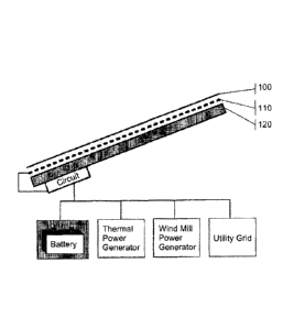
Figure 1 illustrates the principle of the invention, where 100 represents
transparent isolating
coating, 110 conductive coating with different geometries, and 120 the solar
panel or any
surface;
Figures 2 to 8 illustrate different embodiments of conductive coatings;
Figures 9 to 11 illustrate different embodiments of photovoltaic and thermal
solar panels;
Figures 12 and 13 illustrate different embodiments of mirrors and reflectors
for concentrated
solar;
Figures 14 and 15 illustrate embodiments of facades, windows and windshields;
2
CA 2786670 2019-05-16
CA 02786670 2012-07-06
WO 2011/092670 PCT/IB2011/050422
Figure 16 illustrates an embodiment of a vacuum based photovoltaic solar
panel;
Figure 17 illustrates the main electronic board;
Figure 18 illustrates the ultrasonic cleaning system.
The present invention relates to a method and apparatus for levitating and
conveying sand,
dust or melting snow deposits off the surface of objects, in particular solar
panels, mirrors,
glass objects and the like. The principle of a panel according to the present
invention is
illustrated in figure 1, which comprises a panel or any surface on which a
conductive coating
with different geometries is applied, and then on top a transparent isolating
coating is
preferably added.
Accordingly, such apparatus employs various geometries of conductive traces
(either
transparent or opaque) embedded inside a thin layer on the surface of the
object.
This invention employs multiple sensors and detectors used to monitor the
surrounding, the
environment, temperature, humidity and the performance of the object and
activate either the
cleaning or the snow melting process.
The detection system, the embedded traces on the surface and the power output
of the
object (in case of a solar panel) are all connected to an intelligent
electronic board or circuit
that takes decisions when to start any of the processes of cleaning or
melting.
Many objects can be connected together, communicate with each other and are
connected to
a central station for remote monitoring and activation.
Four independent pulsed electrostatic fields, generated from a DC power supply
(all other
known devices use AC power supplies which require much more electronics and
power), use
the geometries of traces on the surface of the objects to repel dirt, dust and
sand without
scratching or damaging the surface of the object. The fields are interlaced
with variable
phase shift to ensure fast execution time.
Additional ultrasonic waves generated by piezoelectric devices placed on the
surface can be
used to provide additional cleaning means of dried humid sand, dust and the
like.
The electronics go to standby or sleep mode when not being used.
Traces and electronics are also used for detecting and melting snow deposit
off the surface
of the object.
This invention saves the use of moving mechanical parts, water, detergent or
any other
cleaning method.
3
CA 02786670 2012-07-06
WO 2011/092670 PCT/IB2011/050422
The power required for the traces on the surface and the electronics is very
small. It can be
drawn from various sources such as:
In the case of a Photovoltaic solar panel less than 10% of its power is
required for less than
one minute at least once a day. Otherwise power can be drawn from a battery,
utility grid or
any other external sources as illustrated in figure 1.
In the case of vacuum or thermal solar panels, power can be drawn from their
own generated
power or any other external sources.
The applications of the present invention are numerous:
-) Photovoltaic solar panels
-) Thermal solar panels
-) Vacuum solar panels
-) Mirrors
-) Glass
-) Windshields
-) Optical surfaces
-) Facades etc.
Figures 2 to 8 illustrate different shapes of conductive traces according to
the present
invention. As can readily be understood from these figures, the shapes can be
different and
have a suitable effect.
Figures 9 to 15 illustrate different embodiments as concrete applications of
the present
invention and the various geometries shown in the figures below and other
similar and
related geometries to cover different shapes of panels and surfaces.
For example, figures 9, 10 and 11 illustrate two embodiments of photovoltaic
and thermal
solar panels. In figure 9, there is a glass 1 or a polymer 6 with patterned,
conductive layer
deposited on either surface, with a highly transparent non-conductive resin 2,
photovoltaic or
thin film solar cells 3 and a back sheet made out of compound material 4.
In figure 10, there is in addition a further highly transparent non-conductive
resin 2 layer and
a thin highly transparent sheet 5 made out of polymers such as Teflon or
another
equivalent material.
In figure 11, there is in addition a honeycomb backing 7 made out of metal for
heat
dissipation or out of other material for high rigidity and lightweight
backing.
Figures 12 and 13 illustrate embodiments for mirrors and reflectors for
concentrated solar
rays.
In addition to the elements already discussed with reference to previous
embodiments such
as the transparent non-conductive resin 2 and the glass or polymer 6 with
patterned,
conductive layer deposited on either surface, there is a highly reflective
parabolic or semi
cylindrical mirror or concentrator 8 in figure 12 and a thermal solar panel
with glass surface 9
in figure 13.
4
CA 02786670 2012-07-06
WO 2011/092670 PCT/IB2011/050422
In figures 14 and 15, embodiments for facades, windows and windshields are
illustrated
where reference 10 identifies a glass sheet and reference 11 identifies double
layer glass
hermetically isolated by a very high vacuum layer for thermal insulation.
In figure 16, an embodiment for vacuum based photovoltaic solar panel is
illustrated. This
embodiment comprises a solar panel 12 made out of a chamber with upper glass
surface
hermetically sealed under very high vacuum for thermal insulation. Solar cells
3 are located
on the bottom layer. The interest of this configuration is that Photovoltaic
cells (or
Polycrystalline Silicon) generates lots of heat especially in hot areas where
the outside
temperature reaches more than 50`C. The efficiency of the cells is reduced by
orders of
magnitude. Vacuum being one of the best insulator will keep the
Polycrystalline silicon at
much lower temperature, therefore higher efficiency.
In figure 17 the electronic means used in the device are illustrated with a
microcontroller, a
high voltage source, monitoring means and communication means to implement the
principle
of the invention.
In figure 18, an embodiment of either a solar panel, mirror, reflector, glass
surface or the like
equipped with either one or multiple piezoelectric devices 13 to create an
ultrasonic cleaning
waves.
In these configurations, the systems include in addition to the elements
already discussed
with reference to previous embodiments such as the transparent non-conductive
resin 2 and
the glass or polymer 6 with patterned, conductive layer deposited on either
surface, there is a
glass sheet 11 used for windshield, window or façade.
The embodiments and example given in the present application are of course
examples that
should not be construed in a limiting manner and combinations of different
embodiments are
possible within the frame of the present invention. Also, it is possible to
use equivalent
means.
Reference numbers
1. Glass with patterned, conductive layer deposited on either surface.
2. Highly transparent non-conductive resin.
3. Photovoltaic or thin film solar cells.
4. Back sheet made out of compound material.
5. Thin highly transparent sheet made out of Polymers such as Teflon.
6. Polymer with patterned, conductive layer deposited on either surface.
7. Honeycomb backing made out of metal for heat dissipation or out of other
material for high
rigidity and light weight backing.
8. Highly reflective parabolic or semi cylindrical mirror or concentrator.
9. Thermal solar panel with glass surface.
10. Glass sheet used for windshield, window or façade.
11. Double layer glass hermetically isolated by a very high vacuum layer for
thermal insulation.
12.A solar panel made out of a chamber with upper glass surface hermetically
sealed under
very high vacuum for thermal insulation. Solar cells are located on the bottom
layer.
13. One or multiple Piezoelectric transducers placed on the panel for creating
an ultrasonic
wave.
100. Transparent isolating coating.
110. Conductive coating with different geometries,
120. Solar panel or any surface
6
CA 2786670 2019-05-16