Note: Descriptions are shown in the official language in which they were submitted.
CA 02787094 2012-07-13
WO 2011/112300 PCT/US2011/023665
1
GRAPHENE BASED THREE-DIMENSIONAL INTEGRATED CIRCUIT DEVICE
BACKGROUND
[0001] The present invention relates generally to semiconductor device
manufacturing
and, more particularly, to a graphene based, three-dimensional (3D) integrated
circuit device.
[0002] Graphene refers to a two-dimensional planar sheet of carbon atoms
arranged in a
hexagonal benzene-ring structure. A free-standing graphene structure is
theoretically stable only
in a two-dimensional space, which implies that a truly planar graphene
structure does not exist in
a three-dimensional space, being unstable with respect to formation of curved
structures such as
soot, fullerenes, nanotubes or buckled two dimensional structures. However, a
two-dimensional
graphene structure may be stable when supported on a substrate, for example,
on the surface of a
silicon carbide (SiC) crystal. Free standing graphene films have also been
produced, but they
may not have the idealized flat geometry.
[0003] Structurally, graphene has hybrid orbitals formed by sp2 hybridization.
In the sp2
hybridization, the 2s orbital and two of the three 2p orbitals mix to form
three sp2 orbitals. The
one remaining p-orbital forms a pi (m)-bond between the carbon atoms. Similar
to the structure
of benzene, the structure of graphene has a conjugated ring of the p-orbitals,
i.e., the graphene
structure is aromatic. Unlike other allotropes of carbon such as diamond,
amorphous carbon,
carbon nanofoam, or fullerenes, graphene is only one atomic layer thin.
[0004] Graphene has an unusual band structure in which conical electron and
hole
pockets meet only at the K-points of the Brillouin zone in momentum space. The
energy of the
charge carriers, i.e., electrons or holes, has a linear dependence on the
momentum of the carriers.
As a consequence, the carriers behave as relativistic Dirac-Fermions with a
zero effective mass
and are governed by Dirac's equation. Graphene sheets may have a large carrier
mobility of
greater than 200,000 cm2/V-sec at 4K. Even at 300K, the carrier mobility can
be as high as
15,000 cm2N-sec.
[0005] Graphene layers may be grown by solid-state graphitization, i.e., by
sublimating
CA 02787094 2012-07-13
WO 2011/112300 PCT/US2011/023665
2
silicon atoms from a surface of a silicon carbide crystal, such as the (0001)
surface. At about
1,150 C, a complex pattern of surface reconstruction begins to appear at an
initial stage of
graphitization. Typically, a higher temperature is needed to form a graphene
layer. Graphene
layers on another material are also known in the art. For example, single or
several layers of
graphene may be formed on a metal surface, such as copper and nickel, by
chemical deposition of
carbon atoms from a carbon-rich precursor.
[0006] Graphene displays many other advantageous electrical properties such as
electronic coherence at near room temperature and quantum interference
effects. Ballistic
transport properties in small scale structures are also expected in graphene
layers.
[0007] Despite the fact that the graphene was isolated for the first time only
a few years
ago (by using ordinary Scotch tape), this field currently being intensively
studied. Because of the
unique electrical properties such as those described above (e.g., high charge
carrier mobility etc.),
graphene is ultimately promising for electronic applications. For example,
graphene transistors
have been demonstrated recently, and more advanced graphene circuits are
considered to be
promising candidates to perhaps replace silicon in future integrated circuit
technology. However,
the lack of easy and low cost graphene fabrication processes presently limits
the development of
graphene applications.
SUMMARY
[0008] In an exemplary embodiment, a three-dimensional (3D) integrated circuit
(IC)
structure includes a first layer of graphene formed over a substrate; a first
level of one or more
active devices formed using the first layer of graphene; an insulating layer
formed over the first
level of one or more active devices; a second layer of graphene formed over
the insulating layer;
and a second level of one or more active devices formed using the second layer
of graphene, the
second level of one or more active devices electrically interconnected with
the first level of one
or more active devices.
[0009] In another embodiment, a method of forming a three-dimensional (3D)
integrated
circuit (IC) structure includes forming a first layer of graphene over a
substrate; forming a first
CA 02787094 2012-07-13
WO 2011/112300 PCT/US2011/023665
3
level of one or more active devices using the first layer of graphene; forming
an insulating layer
over the first level of one or more active devices; forming a second layer of
graphene over the
insulating layer; and forming a second level of one or more active devices
using the second layer
of graphene, the second level of one or more active devices electrically
interconnected with the
first level of one or more active devices.
BRIEF DESCRIPTION OF THE SEVERAL VIEWS OF THE DRAWINGS
[0010] Referring to the exemplary drawings wherein like elements are numbered
alike in
the several Figures:
[0011] Figures 1(a) through 1(h) are a series of cross-sectional views
illustrating an
exemplary method of forming a graphene based, three-dimensional (3D)
integrated circuit, in
accordance with an embodiment of the invention; and
[0012] Figures 2(a) through 2(k) are a series of cross-sectional views
illustrating an
exemplary method of forming a graphene based, 3D integrated circuit, in
accordance with an
alternative embodiment of the invention.
DETAILED DESCRIPTION
[0013] Disclosed herein are embodiments of a graphene based, three-dimensional
(3D)
integrated circuit device, and methods of forming the same. In the
semiconductor industry, a 3D
integrated circuit (IC) generally refers to a chip having two or more layers
of active electronic
components, integrated both vertically and horizontally into a single circuit.
3D ICs potentially
offer many significant benefits, such as for example: a smaller footprint
(more functionality
fitting into a small space), speed (the average wire length becomes much
shorter, in turn reducing
signal propagation delay and increasing overall performance), power
consumption (by keeping a
signal on-chip, the resulting shorter wires reduce power consumption and
produce less parasitic
capacitance), and heterogeneous integration, to name a few. In the case of
heterogeneous
integration, different circuit layers may be formed with different processes,
or even on different
types of wafers. Moreover, components otherwise having completely incompatible
manufacturing processes could be combined in a single device.
CA 02787094 2012-07-13
WO 2011/112300 PCT/US2011/023665
4
[0014] Currently, 3D ICs may be formed by techniques such as wafer-on-wafer
bonding,
wherein electronic components are built on two or more semiconductor wafers,
which are then
aligned, bonded, and diced into 3D ICs. Each wafer may be thinned before or
after bonding.
Vertical connections are either built into the wafers before bonding or
otherwise created in the
stack after bonding. These "through-silicon vias" (TSVs) pass through the
silicon substrate(s)
between active layers and/or between an active layer and an external bond pad.
In a die-on-wafer
process, electronic components are built on two semiconductor wafers. One
wafer is diced, and
the singulated dies are aligned and bonded onto die sites of the second wafer.
As in the wafer-
on-wafer method, thinning and TSV creation are performed either before or
after bonding.
Additional dies may be added to the stacks before dicing. Alternatively, in a
die-on-die process,
electronic components are built on multiple dies, which are then aligned and
bonded. Thinning
and TSV creation may be done before or after bonding.
[0015] In order to avoid multiple substrates and aligning, thinning, bonding,
or TSV
techniques, 3D ICs would desirably be formed monolithically. That is, the
electronic
components and their connections (wiring) are built in layers on a single
semiconductor wafer,
which is then diced into 3D ICs. Unfortunately, existing applications of this
method are
currently limited because creating conventional transistors in semiconductor
layers (e.g., dopant
implantation and activation annealing) requires processing tempeatures that
are sufficient any
existing wiring.
[0016] Accordingly, Figures 1(a) through 1(h) are a series of cross-sectional
views
illustrating an exemplary method of forming a graphene based, three-
dimensional (3D) integrated
circuit. Beginning in Figure 1(a), a starting substrate 102 (e.g., silicon)
has an insulating layer
(e.g., an oxide such as Si02) 104 formed thereon. In Figure 1(b), a blanket
graphene layer 106 is
transferred onto the insulating layer 104. The transfer of graphene films may
be performed in
any suitable manner known in the art such as, for example, by a dry thermal
release tape process.
In one exemplary embodiment, the graphene layer 106 is a monolayer of
graphene. Notably,
because graphene is deposited on such a substrate surface in this manner, it
is a particularly
suitable material for 3D integration.
[0017] As shown in Figure 1(c), the graphene layer 106 is patterned through
appropriate
CA 02787094 2012-07-13
WO 2011/112300 PCT/US2011/023665
lithography techniques (e.g., hardmask and/or photoresist layer formation,
development and
etching) to form desired active areas of graphene-based devices. This is
followed by a first level
of transistor device formation. As shown in Figure 1(d), the graphene active
areas 106 are
covered with transistor gate stack materials such as, for example, a gate
dielectric layer 108 and a
gate electrode layer 110. In an exemplary embodiment, the gate dielectric
layer 108 may be a
high-k material suchas hafnium, hafnium silicate, zirconium oxide, zirconium
silicate, nitrided
dielectrics, as well as combinations thereof. The gate electrode layer 110 may
include
polysilicon, a metal, or combinations thereof.
[0018] Referring now to Figure 1(e), the gate dielectric and gate electrode
layers 108, 110
are then patterned so as to define transistor devices (e.g., field effect
transistors or FETs) on the
patterned graphene active areas 106, including gate electrodes 112 and gate
dielectric layers 114.
It should be noted that the patterning operation depicted in the figures is
only illustrative in
nature, in that more than one patterning and RIE process may be used, for
example, in
accordance with different gate stack requirements depending on the type and
polarity of the
transistor device. Thus, in the exemplary embodiment shown, the designation
"GN" refers to a
transistor gate for an n-type device (e.g., an NFET) while the designation
"GP" refers to a
transistor gate for a p-type device (e.g., a PFET).
[0019] Following gate stack patterning, the formation of source/drain contacts
116 and
conductive pad structures 118 is shown in Figure 1(f). The formation of the
source and drain
contacts includes, for example deposition of source/drain contact material and
patterning. The
source/drain contact material may be a metal material such as, for example,
titanium (Ti),
palladium (Pd), aluminum (Al), tungsten (W), or alloys thereof. The deposition
method can be
may include, for example, sputtering, and atomic layer deposition (ALD).
[0020] Upon completion of a first layer of graphene circuit devices, an
insulating layer
120 (e.g., an oxide) is formed over the devices as shown in Figure 1(g). Vias
122 are then etched
into the insulating layer 120 so as to provide vertical electrical connection
to one or more
additional levels of graphene based active devices, in accordance with a 3D IC
structure. In
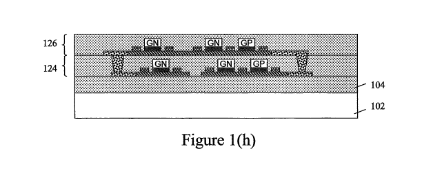
Figure 1(h), the lower level 124 of graphene based active devices is shown
connected to an upper
layer 126 of graphene based active devices. The formation of the upper level
126 is similar to
CA 02787094 2012-07-13
WO 2011/112300 PCT/US2011/023665
6
that of the lower level 124, in that a graphene layer (e.g., monolayer) is
first deposited/transferred
onto the completed lower level 124, followed by pattering of the desired
active areas of the
graphene, formation and patterning of the gate stack materials, formation and
patterning of the
source/drain contacts and conductive pads, and formation of an insulating
layer over the upper
level devices.
[00211 Although the illustrative embodiment depicts a pair of graphene based
active
device levels, it will be appreciated that the above process may be repeated
as desired to form
still additional graphene based active device levels. In one contemplated
embodiment, each level
of graphene may have different functions (e.g., logic, analog, memory).
[00221 The exemplary 3D IC device embodiment shown in the process flow
sequence of
Figures 1(a) through 1(h) is an example of a top gate orientation, in that the
gate electrode and
dielectric are disposed above the active graphene source/drain regions.
However, the active
graphene devices may also be formed using a bottom orientation, as depicted in
the process flow
sequence of Figures 2(a) through 2(k). Beginning in Figure 2(a), a starting
substrate 202 (e.g.,
silicon) has an insulating layer (e.g., an oxide such as Si02) 204 formed
thereon, similar to the
top gate orientation process of Figure 1(a).
[00231 Rather then transferring a graphene layer to the insulating layer 204
at this point in
the process, the insulating layer 204 is instead patterned with vias 206
corresponding to the
locations of the gates of the lower level graphene based devices, as shown in
Figure 2(b). Then,
as shown in Figure 2(c), a gate electrode layer 208 is formed over the device,
filling in the vias.
Once the gate electrode layer 208 is planarized, individual gate electrodes
210 are now defined,
as shown in Figure 2(d). A gate dielectric layer 212 is then formed over the
insulating layer 204
and gate electrodes 210, as shown in Figure 2(e). As is the case with the
first embodiment, the
gate dielectric layer 212 may be a high-k gate dielectric layer.
[00241 Referring now to Figure 2(f), a graphene layer 214 is formed on the
gate dielectric
layer 212. Again, the transfer of graphene films may be performed in any
suitable manner known
in the art such as, for example, by a dry thermal release tape method. In one
exemplary
embodiment, the graphene layer 214 is a monolayer of graphene. As also shown
in Figure 2(f),
CA 02787094 2012-07-13
WO 2011/112300 PCT/US2011/023665
7
the gate electrodes have been labeled with "GN" and "GP" designations to
indicated exemplary
n-type and p-type FET devices.
100251 In Figure 2(g), the graphene layer is patterned in accordance with the
desired
active areas, and corresponding to the location of the bottom orientation gate
electrodes. The
blanket gate dielectric layer 212 remains intact at this point. As then shown
in Figure 2(h),
source/drain contacts 216 for the graphene based FET devices are formed,
followed by gate
dielectric layer patterning and formation of conductive pads 218 as
illustrated in Figure 2(i).
Thus configured, a first or lower layer of graphene based active devices is
completed, and
followed by the formation of an insulating layer 220 (e.g., an oxide) over the
devices as shown in
Figure 2(j). Vias 222 are then etched into the insulating layer 220 so as to
provide vertical
electrical connection to one or more additional levels of graphene based
active devices, in
accordance with a 3D IC structure. Finally, in Figure 2(k), a second level 224
of graphene based
active devices is shown connected to the first level of graphene based active
devices. Here, the
FET devices of the second level 224 are also bottom orientation gates.
However, it is still further
contemplated that a graphene based 3D IC structure could have both top
orientation and bottom
orientation gates in the same or different levels of the device.
[00261 While the invention has been described with reference to a preferred
embodiment
or embodiments, it will be understood by those skilled in the art that various
changes may be
made and equivalents may be substituted for elements thereof without departing
from the scope
of the invention. In addition, many modifications may be made to adapt a
particular situation or
material to the teachings of the invention without departing from the
essential scope thereof.
Therefore, it is intended that the invention not be limited to the particular
embodiment disclosed
as the best mode contemplated for carrying out this invention, but that the
invention will include
all embodiments falling within the scope of the appended claims.