Note: Descriptions are shown in the official language in which they were submitted.
CA 02787221 2012-07-16
WO 2011/086394 1
PCT/GB2011/050077
1 Gas Sensor with Radiation Guide
2
3 Field of the invention
4
The invention relates to the field of optical absorption gas sensors,
including but not
6 limited to infra-red absorption gas sensors.
7
8 Background to the invention
9
Gas sensors are commonly employed in industrial and consumer applications to
11 measure analytes in the gaseous state. Many gas sensors rely on the
absorption
12 characteristics of the target analyte when illuminated with radiation
and comprise a
13 radiation source, a detector capable of detecting radiation emitted by
the radiation
14 source, and a chamber for receiving the target gaseous analyte. Analyte
gas within
the chamber absorbs radiation of specific wavelengths or ranges of wavelengths
and
16 the attenuation of the radiation detected by the detector gives an
indication of the
17 concentration of the target analyte within the chamber. The target
analyte typically
18 diffuses into the chamber although sensors which actively transport gas
into the
19 chamber are known. In some optical absorption gas sensors, the source
emits
radiation at a broad range of wavelengths and a wavelength selective filter is
21 provided at the detector, in which case the gas sensor is referred to as
a non-
22 dispersive sensor. In other optical absorption gas sensors, the source
emits radiation
23 of a defined wavelength or wavelength range or includes a filter which
selects a
24 specific wavelength band.
CA 02787221 2012-07-16
WO 2011/086394 2
PCT/GB2011/050077
1
2 To achieve
high sensitivity, it is desirable that the radiation has as long a mean path
3 length as
possible through the analyte, from the radiation source to the detector, such
4 that the
analyte absorbs a significant portion of the radiation, and that the radiation
is
not absorbed by any other processes within the sensor. For example, if the
path
6 between the
radiation source and the detector is not linear, the radiation must be
7 reflected to
be directed to the detector. However, the reflecting surface will introduce
8 optical loss
from absorption and/ or scatter and this optical loss will typically be
9 significant
in a low cost sensor. There is therefore a balance to be struck between
increasing the number of reflections to increase path length and avoiding
excessive
11 attenuation of the emitted radiation by excessive reflections.
12
13 However, for
many practical applications, it is desirable for gas sensors to be small,
14 or to comply
with standardised dimensions, resulting in generally short path lengths
and corresponding low sensitivity. Thus, one aim of the present invention is
to
16 provide a gas
sensor that has high sensitivity whilst being compact and suitable for
17 cost-effective manufacture.
18
19 It is known
to provide gas sensors having a straight hollow tubular radiation guide
which extends between the radiation source and the detector and has a
rectangular
21 or other
cross section. Radiation guides of this type guide radiation with a range of
22 path lengths
depending on the orientation at which radiation enters the radiation
23 guide.
Radiation which enters the radiation guide at a high angle of incidence to the
24 walls of the
radiation guide reflects many times and so is more highly attenuated than
radiation which enters a straight rectangular radiation guide at an
orientation close to
26 the axis of the radiation guide.
27
28 It is known
that for linear radiation guides increasing the size of the cross section
29 decreases the
number of reflections and therefore the absorption loss but results in
poor collection efficiency. A better arrangement is to have the beginning and
end of
31 the waveguide
shaped eg as compound parabolic collectors (CPCs). The effect of
32 this is to
transform the radiation field as it moves along the waveguide. At the source
33 it has a
large angular spread and relatively small spatial spread, midway it has a
34 small angular
spread but large spatial spread and at the detector again it has a large
angular spread but small spatial spread. If chosen correctly this arrangement
can
36 significantly reduce the absorption due to multiple reflections.
37
CA 02787221 2012-07-16
WO 2011/086394 3
PCT/GB2011/050077
1 The
incorporation of a curved portion into a radiation guide can facilitate the
provision
2 of a longer
path for radiation in a given volume than a radiation guide lacking curved
3 portions.
However, where a radiation guide curves, radiation falling on the curved
4 walls of the
guide results in greater angular spread without a reduction in spatial
spread and consequently an increase in loss due to absorption in the multiple
6 reflections.
In particular, where radiation falls onto a curved wall, parallel radiation
7 incident on
the curved wall will not be parallel after reflection and so be dispersed.
8 Some
radiation will be incident on a curved wall with a greater angle of incidence
9 than would be
the case were the wall planar. Thus, where a radiation guide curves,
some radiation is reflected into a path where it reflects at a relatively high
angle
11 towards an
opposite wall, with the effect that a substantial proportion of radiation
12 entering a
curved radiation guide may be reflected many times and so be strongly
13 absorbed.
14
Furthermore, in embodiments comprising a curved radiation guide and a
collector at
16 the detector,
the collimator is unable to direct the radiation onto the detector due to
17 the increase
in angular spread. Therefore, the intensity of radiation incident upon the
18 detector is reduced, correspondingly reducing the sensitivity of the gas
sensor.
19
Some aspects of the invention aim to provide optical absorption gas sensors
with
21 improved
curved radiation guides which better transmit radiation from a radiation
22 source to a detector through a gas sample.
23
24 Another
problem which arises in the field of absorption gas sensors is that during
operation the radiation source, which is often an infra-red radiation emitter,
and the
26 detector are
temperature sensitive. The emission spectrum of the radiation source
27 may vary with
temperature and the sensitivity of the detector may also vary with
28 temperature.
As well as being affected by ambient temperature, the radiation source
29 in particular
will heat up in use. If the radiation output is to be substantial and pulsed,
temperature may fluctuate dramatically. When measuring small attenuations,
small
31 measurement
errors due to temperature fluctuations in either or both the source and
32 the detector can create substantial errors in measured gas
concentration.
33
34 WO
2007/091043 (Gas Sensing Solutions Limited) discloses a sensor in which an
infra-red light emitting diode (functioning as radiation source) and a
photodiode
36 (functioning
as detector) are located adjacent to each other and in thermal
37 communication
with each other. By locating the source and detector adjacent to
CA 02787221 2012-07-16
WO 2011/086394 4
PCT/GB2011/050077
1 each other
and in thermal communication, they remain at substantially the same
2 temperature,
simplifying the procedure of compensating for temperature variation.
3 Accordingly,
some embodiments of the invention aim to provide a compact gas
4 sensor having
high sensitivity given the constraint that the source and detector
should be either or both adjacent either other and in thermal communication.
6
7 Optical
absorption gas sensors typically include a mechanism for providing a
8 reference
signal, in addition to a measurement signal, to enable more accurate
9 measurement.
One mechanism for obtaining a reference signal in a non-dispersive
optical absorption sensor is to provide a second detector, with a different
filter, to
11 measure light
at a wavelength which is not absorbed by any gas which is expected to
12 be present in
varying amounts. However, this adds to the complexity of the gas
13 sensor, and
therefore its cost. It is known to provide separate measurement and
14 reference
radiation sources, but there will typically be different paths between these
sources and the detector, or the presence of a reference radiation source will
require
16 an optical
arrangement which directs a lower proportion of emitted radiation to the
17 detector than
would be the case without the presence of a second radiation source.
18 Accordingly,
some aspects of the invention aim to provide improved or alternative
19 mechanisms for obtaining a reference signal in an optical absorption gas
sensor.
21 Summary of the invention
22
23 According to
the first aspect of the invention there is provided a gas sensor
24 comprising a
radiation source, a detector operable to detect radiation emitted by the
radiation source and a radiation guide operable to guide radiation between the
26 radiation
source and the detector, the radiation guide comprising a curved portion
27 having a
substantially rectangular cross section, wherein the curved portion of the
28 radiation
guide curves around an axis parallel to one of the sides of the rectangular
29 cross section.
31 The
substantially rectangular cross section may be a substantially square cross
32 section (for
example, a square cross section), but preferably the rectangular cross
33 section is a
substantially oblong cross section (for example, an oblong cross section)
34 having a major and a minor dimension.
36 As the curved
portion has a substantially rectangular cross-section and curves
37 around an
axis parallel to one of the sides of the rectangular cross-section, the
CA 02787221 2012-07-16
WO 2011/086394 5
PCT/GB2011/050077
1 angular
spread of the radiation will be increased and some radiation will be reflected
2 into paths
where it is will be reflected many times (and thereby highly attenuated in a
3 radiation
guide which significantly absorbs incident radiation). However, this effect
4 will occur in
only one plane. Radiation which reflects off the walls which are normal
to the axis around which the radiation guide curves will not be dispersed in
this way.
6 Thus, the
amount of radiation which reaches the detector is greater than would be the
7 case if the
radiation guide did not have a rectangular cross section and curved
8 around an axis parallel to one of the side of the rectangular cross
section.
9
Preferably, the radiation guide comprises a collimator operable to at least
partially
11 collimate
radiation emitted by the radiation source. Typically, the collimator reduces
12 the angular
spread of radiation more in an axis parallel to the major dimension than
13 an axis parallel to the minor dimension of the radiation guide.
14
Preferably, the radiation guide comprises a condenser operable to condense
16 radiation onto the detector.
17
18 The curved
portion of the radiation guide increases the angular spread of the
19 radiation in
the plane of curvature only. Therefore, there is a disparity in angular
spread for radiation reflected predominantly by the walls parallel to the
minor
21 dimension of
the rectangular cross section and radiation reflected predominantly by
22 the walls
parallel to the major dimension of the rectangular cross section incident
23 upon the
condenser. The direction radiation incident to the condenser is condensed
24 is determined
by the angular spread of that radiation. Generally, the condenser will
be optimised to direct radiation with the lower angular spread onto the
detector.
26 Therefore,
radiation reflected predominantly by the walls parallel to the major
27 dimension of
the rectangular cross section, having a high angular spread, may not
28 reach the detector.
29
Radiation having a high angular spread before being reflected within a curved
31 radiation
guide can be collected more efficiently by a condenser than collimated
32 radiation having a low angular spread.
33
34 Therefore, in
the present aspect of the invention, the collimator typically collimates
the radiation emitted by the radiation source to a greater degree in the axis
parallel to
36 the major
dimension of the rectangular cross section where reflections from the walls
37 perpendicular
to this axis will not generally introduce angular spread, and to a lesser
CA 02787221 2012-07-16
WO 2011/086394 6
PCT/GB2011/050077
1 degree in the
axis parallel to the minor dimension of the rectangular cross section
2 where
reflections from the walls perpendicular to this axis will generally introduce
3 angular spread.
4
Accordingly, the current aspect of the invention combines a long path length
provided
6 by a curved
portion of the radiation guide and a high proportion of radiation emitted
7 by the radiation source reaching the detector, leading to high
sensitivity.
8
9 The curved
portion of the radiation guide may curve around an axis parallel to the
minor dimension of the substantially rectangular cross section. However,
preferably,
11 the curved
portion of the radiation guide curves around an axis parallel to the major
12 dimension of
the substantially rectangular cross section. Thus, for a given cross-
13 sectional
area (and therefore volume of gas through which radiation passes)
14 dispersion
and attenuation will be less than would be the case if the curvature was
around an axis parallel to the minor dimension or if the radiation guide has a
16 substantially square cross section.
17
18 Preferably,
the radiation guide, and the curved portion of the radiation guide,
19 comprises a
hollow tube. The interior of the radiation guide is in gaseous
communication with air adjacent the gas sensor. Analyte gas is received within
the
21 hollow tube
in use, through one or more apertures or gas permeable regions of the
22 radiation
guide. The radiation guide may have an inward facing surface formed from
23 a material
operable to reflect radiation emitted by the radiation source. The material
24 may be a
metallic coating, such as gold or aluminium. The material may be a
dielectric coating. By enabling the use of materials which absorb some
incident
26 radiation the
invention allow cost-effective sensors to be provided. Typically, the
27 reflectivity of the material is at least 0.99, or typically at least
0.97.
28
29 The radiation
source and the detector may be adjacent to each other. The spacing
between the radiation source and the detector may be less than three times,
and
31 preferably
less than two times, the mean breadth of the radiation guide in a plane
32 extending
through the radiation source and the detector (which may also be a plane
33 of symmetry
of the radiation guide). The shortest path length of radiation between
34 the radiation
source and the detector along the radiation guide is preferably at least
10 times (18 times in an example embodiment) the spacing between the radiation
36 source and
the detector. Thus, a significant path length is obtained while the
37 radiation source and detector are close to each other.
CA 02787221 2012-07-16
WO 2011/086394 7
PCT/GB2011/050077
1
2 The radiation
source and the detector may be in thermal communication with each
3 other, for
example, directly or through heat transfer means. The radiation source and
4 the detector
may be in thermal communication so that, in use, the radiation source
and the detector remain substantially in thermal equilibrium.
6
7 The gas
sensor may comprise a support element, which may be a planar support,
8 with the
radiation source and detector mounted on the support element. The support
9 element may
comprise an electronic circuit and is typically a printed circuit board
(PCB). The support element may further comprise heat transfer means operable
to
11 conduct heat
between the radiation source and the detector. The heat transfer
12 means may be the electrical circuit.
13
14 The radiation
guide may comprise a plurality of said curved portions. The radiation
guide may comprise first and second curved portions which curve in opposite
senses.
16 Preferably,
the radiation guide comprises a first curved portion which curves in a first
17 sense and
then a second curved portion, further along the radiation guide than the
18 first curved
portion (measured from the radiation source to the detector) which curves
19 in a second
opposite sense. The radiation guide may further comprise a third curved
portion, further along the radiation guide than the second curved portion
(measured
21 from the
radiation source to the detector) curved in the first sense. This enables a
22 longer
radiation path to be provided in a given volume, particularly in embodiments
23 where light
is incident on the detector in generally the opposite direction to the
24 direction at which light enters the radiation guide from the radiation
source.
26 The radiation
guide may comprise a first curved portion which curves in a first sense
27 by at least
10 , and typically by at least 25 , and a second curved portion, further
28 along the
radiation guide than the first curved portion (measured from the radiation
29 source to the
detector) which curves in the opposite sense with a substantially
constant curve for at least 180 . The first and second curved portions may be
in
31 direct contact with each other.
32
33 The radiation
guide may extend substantially in a plane. The radiation guide may
34 have a plane
of symmetry. The curved portion of the radiation guide may curve
within a plane.
36
CA 02787221 2012-07-16
WO 2011/086394 8
PCT/GB2011/050077
1 The radiation
guide may change the mean direction of radiation between the radiation
2 source and
the detector by at least 900. The radiation guide may change the mean
3 direction of
radiation between the radiation source and the detector by at least 135 .
4 In
embodiments in which the detector receives radiation with a mean direction
which
is substantially opposite the mean direction at which radiation from the
radiation
6 source enters
the radiation guide the radiation guide may change the mean direction
7 of radiation
between the radiation source and the detector by 160-200 and
8 preferably 170-190 or more preferably 175-185 .
9
The integral of magnitude of the curvature of the radiation guide may be at
least 90 ,
11 preferably at
least 180 and more preferably at least 260 . The integral of the
12 magnitude of
the curvature of the radiation guide is preferably at least 90 greater
13 than the net
curvature of the radiation guide between the radiation source and the
14 detector.
Thus, it may be possible to provide a mean path length which is greater
than if the radiation guide curved continuously in a single sense between the
16 radiation
source and the detector. Nevertheless, it may be that the integral of the
17 magnitude of
the curvature of the radiation guide is less than 720 or more preferably
18 less than 540 to avoid excess attenuation of radiation.
19
The radiation guide may comprise a collimator operable to at least partially
collimate
21 radiation
emitted by the source. By at least partially collimating radiation emitted by
22 the source,
the amount of light lost due to attenuation by multiple reflections in the
23 curved
portion of the radiation guide is reduced. Preferably, the collimator is a
partial
24 collimator
which partially reduces the angular spread of radiation. It is preferable for
radiation to be directed through as much as possible of the volume of the
radiation
26 guide to
maximise absorption by analyte gas. Furthermore, although radiation which
27 is incident
at a significant angle to the flat walls of the curved portion will be
reflected
28 a significant
number of times, it will have a greater path length than radiation which is
29 parallel to
the flat walls of the curved portion. Accordingly, the collimator preferably
partially collimates the radiation.
31
32 The
collimator may be a reflector, for example, a parabolic reflector, and is
typically
33 part of the
reflective interior surface of the radiation guide. At least part of the
curved
34 portion of
the radiation guide may be at least part of the collimator. The collimator
may be a lens or an array of lenses. Typically, the collimator has a
substantially
36 oblong cross
section having a minor and a major dimension and the collimator
37 reduces the
angular spread of radiation more in an axis parallel to the major
CA 02787221 2012-07-16
WO 2011/086394 9
PCT/GB2011/050077
1 dimension
than an axis parallel to the minor dimension. Preferably, the major
2 dimension of
the collimator and the major dimension of the or each curved portion of
3 the radiation guide are parallel.
4
The collimator may extend for more than 5%, or preferably more than 10%, of
the
6 length of the
radiation guide. We have found that collimators of this length provide a
7 suitable degree of collimation for the present aspect of the invention.
8
9 The radiation
guide may comprise a condenser operable to condense radiation onto
the detector. The condenser may be a reflector, for example a parabolic
reflector or
11 an elliptical
reflector. However, the condenser may comprise a lens or an array of
12 lenses.
13
14 The condenser
may extend for more than 5%, or preferably more than 10%, of the
length of the radiation guide.
16
17 The or each
curved portion of the radiation guide typically comprises an inner wall
18 and an
opposed outer wall such that the inner wall describes the inner arc of the
19 curved
portion and the opposed outer wall describes the outer arc of the curved
portion. It may be that the inner wall of one or more said curved portions
comprises
21 an inlet to
admit a gas sample into the radiation guide. Typically, less radiation falls
22 on the inner
wall of a curved portion of a radiation guide and, by providing an inlet for
23 a gas sample
in the inner wall of a curved portion of the radiation guide, the
24 attenuation
of radiation within the radiation guide by the inlet for a gas sample is less
than would be the case if the inlet was provided in the outer wall. This is
especially
26 beneficial
where the curved portion curves by more than 90 or preferably more than
27 180 .
28
29 The or each
curved portion of the radiation guide may comprise an inward region and
an outward region. The inner region of the radiation guide may correspond to
that
31 half of the
radiation guide nearest the inner wall. The outward half of the radiation
32 guide may
correspond to that half of the radiation guide nearest the outer wall.
33 Radiation
travelling from the radiation source to the detector through the radiation
34 guide may
travel around the curved section of the radiation guide predominantly
within the outward region of the radiation guide, as a result of the
configuration of the
36 radiation
guide, the radiation source and the detector. This reduces the mean
37 number of reflections of the radiation between the radiation source and
the detector.
CA 02787221 2012-07-16
WO 2011/086394 10
PCT/GB2011/050077
1
2 The width of the radiation guide may be less than one tenth the length of
the radiation
3 guide (measured along the centre of the radiation guide) but is
preferably less than
4 one twentieth the length of the radiation guide.
6 The gas sensor may comprise a radiation filter which selectively admits
radiation
7 within a defined wavelength range into the detector. The wavelength range
is
8 selected depending on the target analyte. Typically, the target analyte
is a gaseous
9 species such as CO2, CO, NO, CH4 or NO2 etc.
11 The gas sensor may comprise a radiation filter which selectively admits
radiation
12 within a defined wavelength range at the radiation source.
13
14 The radiation source and or the detector may be chosen such that the
radiation
emitted or detected respectively coincides with a wavelength absorption peak
of the
16 target analyte to be detected.
17
18 The gas sensor may be a non-dispersive infra-red sensor. Typically, the
majority of
19 the radiation emitted by the radiation source is near infra red.
21 The radiation source may be a light-emitting diode (LED), an organic
LED, a laser
22 diode or another electrical component operable to convert electrical
current into
23 radiation. The radiation source may emit radiation in a broad
spectrum of
24 wavelengths. The radiation source may emit radiation in a narrow
spectrum of
wavelengths. Typically, the radiation source has a peak emission wavelength
that
26 overlaps with the absorption spectrum of the target analyte such that
the target
27 analyte may strongly absorb the radiation emitted by the radiation
source.
28
29 The detector may be a photodiode. Alternatively, the detector may be a
device
operable to convert incident radiation into thermal energy and subsequently
convert
31 the thermal energy into electrical current. For example, the device may
be a
32 thermopile or pyroelectric detector.
33
34 The gas sensor may comprise a radiation guide element (comprising or
consisting of
the said radiation guide) and the abovementioned support element. The
radiation
36 guide element or the support element may comprise a plurality of
locating elements
37 configured to locate the support element relative to the radiation guide
element (and
CA 02787221 2012-07-16
WO 2011/0863941 1
PCT/GB2011/050077
1 to thereby
align the detector and radiation source with the radiation guide). Some or
2 all of the
locating elements may comprise a protrusion or groove on the radiation
3 guide
element. In at least some cases, the support element may comprise a
4 cooperating
groove or protrusion respectively. Preferably, there will be three locating
elements (formed in the radiation guide element or the support element).
Typically
6 there will be
a cooperating groove or protrusion for two of the three locating elements
7 (formed in
the support element or radiation guide element respectively). This enables
8 the relative
movement of the radiation guide element and the support element to be
9 fully constrained without being overconstrained.
11 The plurality
of locating elements may comprise a pivot (.e.g a protuberance received
12 by a
complementary recess) in the radiation guide element (or support element)
13 around which
the radiation guide element can be rotated relative to the support
14 element
during the process of locating the radiation guide element relative to the
support element. The pivot may comprise a hemisphere or other protrusion.
16
17 The plurality
of locating elements may comprise at least one protrusion (such as a
18 post) in the radiation guide element (or support element) received by a
19 complementary
formation (for example, a groove) in the support element (or radiation
guide element respectively) and configured to prevent rotation of the support
element
21 relative to
the radiation guide element in the plane normal to the radiation guide. The
22 complementary
formation in the support element may be elongate. The elongate
23 complementary
formation may allow the support element or radiation guide element
24 to expand
(for example due to a rise in temperature) relative to the radiation guide
element or support element respectively without relative rotation between the
support
26 element and the radiation guide element.
27
28 The plurality
of locating elements may comprise at least one spacer. The at least one
29 spacer may be
located such that when the support element is mounted onto the
radiation guide element the at least one spacer is between the detector and
the
31 radiation
source. The at least one spacer may be configured to maintain a specified
32 separation
between the support element and the radiation guide element. The at
33 least one
spacer may be adapted to maintain a specified separation between the
34 detector and the radiation source, and radiation guide of the radiation
guide element.
36 Preferably,
the at least one spacer is not received by a cooperating groove but abuts
37 the opposing
surface. For example, in embodiments where the spacer is located on
CA 02787221 2012-07-16
WO 2011/086394 12
PCT/GB2011/050077
1 the radiation
guide element, the spacer abuts the support element and is not received
2 by a cooperating groove.
3
4 The provision
of a plurality of locating elements configured to locate the support
element to the gas sensor allows the radiation source and the detector to be
located
6 precisely to
the gas sensor such that the radiation source is adjacent to an aperture in
7 the radiation
guide and the detector is adjacent to an aperture in the radiation guide
8 or to otherwise align the radiation source and detector relative to the
radiation guide.
9
Preferably, the gas sensor comprises three locating elements. Preferably, the
three
11 locating
elements comprise a pivot, a protrusion and a spacer. The three locating
12 elements may
be arranged to form the corners of a triangle, that is, with one of the
13 locating elements located out of line with the other two.
14
Preferably, the gas sensor comprises biasing means (e.g. a biasing device) to
bias
16 the support
element towards the radiation guide element. The biasing means may be
17 a rigid or
flexible element (such as a spring) which applies pressure onto the support
18 element
towards the radiation guide element. This enables the locating elements to
19 constrain the
relative position and orientation of the radiation guide element and the
support element.
21
22 The provision
of a biasing means ensures that the plurality of locating elements
23 remain
engaged with their respective cooperating grooves and surfaces, thereby
24 ensuring that
the support element is stably constrained against the radiation guide
element, thus maintaining the alignment of the radiation guide and the
detector with
26 the radiation guide.
27
28 The radiation
guide may comprise a support element facing surface. A recess may
29 be formed in
the support element facing surface adjacent to the radiation source. A
recess may be formed in the support element facing surface adjacent to the
detector.
31 The recess
formed in the support element facing surface adjacent to the radiation
32 source and/or
the detector may be located such that there is a separation between
33 the radiation
source and or the detector, and the support element facing surface of
34 the radiation guide.
36 In
embodiments of the invention where the radiation guide comprises a conductive
37 surface
(typically, a metal coating, for example, gold), provision of a recess formed
in
CA 02787221 2012-07-16
WO 2011/086394 13
PCT/GB2011/050077
1 the support
element facing surface adjacent to the radiation source and or the
2 detector
prevents an electrical short circuit being formed between the radiation guide
3 and the
radiation source or detector. This is applicable where the support element
4 facing
surface forms at least part of the conductive surface of the radiation guide.
This is especially advantageous where the detector and/or radiation guide
element
6 has a
radiation guide facing surface and an electrical connection (e.g. a connection
to
7 a wire extending to a circuit board) on the respective radiation guide
facing surface.
8
9 According to
a second aspect of the invention a gas sensor is provided comprising a
radiation source, a detector operable to detect radiation emitted by the
radiation
11 source and a
radiation guide operable to guide radiation between the radiation source
12 and the
detector, wherein the detector is operable to emit radiation having a
different
13 wavelength
spectrum to that emitted by the radiation source, and the radiation source
14 is operable to detect radiation emitted by the detector.
16 Preferably,
the gas sensor may further comprise an electronic circuit operable to
17 cause the
radiation source and the detector to operate in two modes such that in a
18 first mode
the radiation source emits radiation and said radiation is detected by the
19 detector to
provide a measurement signal, and in a second mode the detector emits
radiation and said radiation is detected by the radiation source to provide a
reference
21 signal.
22
23 Accordingly,
the present aspect of the invention allows a reference signal and a
24 measurement
signal to be obtained along the same radiation path without the
requirement of providing a separate radiation source and a separate detector.
A gas
26 sensor
comprising a first and a second radiation source, and a first and a second
27 detector will
be larger than a gas sensor comprising a single radiation source and a
28 single
detector. Therefore, providing a radiation source and a detector that are each
29 operable to
emit radiation and to be sensitive to radiation emitted by the other
enables the gas sensor of the present aspect of the invention to be smaller
than gas
31 sensors requiring an additional radiation source and detector.
32
33 Preferably,
radiation emitted by the detector and detected by the radiation source
34 provides a
reference signal and the radiation emitted by the radiation source and
detected by the detector provides a measurement signal. Typically the detector
and
36 radiation
source emit radiation with different peak wavelengths. Typically, the
37 radiation
source emits radiation having a peak intensity at a wavelength substantially
CA 02787221 2012-07-16
WO 2011/086394 14
PCT/GB2011/050077
1 corresponding
to a wavelength at which a target analyte gas absorbs radiation.
2 Typically the
detector emits radiation predominantly at wavelengths which are
3 substantially
less absorbed by a target analyte than the said wavelength of the peak
4 intensity of radiation emitted by the radiation source.
6 Optional
features described in relation to the first or second aspect of the invention
7 are optional
features of the second aspect of the invention and the gas sensor of the
8 first aspect
of the invention may also be a gas sensor according to the second aspect
9 of the invention.
11 According to
a third aspect of the invention there is provided a gas sensor comprising
12 a first
radiation source, a second radiation source, a detector operable to detect
13 radiation
emitted by the first radiation source and the second radiation source, and a
14 radiation
guide operable to guide radiation from the first radiation source and the
second radiation source to the detector, wherein radiation emitted from the
second
16 radiation
source is guided along a path extending either or both around or through the
17 first radiation source.
18
19 Radiation
detected from the first radiation source may be used to calculate a
measurement or a reference signal in use. Radiation detected from the second
21 radiation
source may be used to calculate a reference or a measurement signal
22 respectively.
Thus, the second radiation source typically emits radiation with a
23 different wavelength spectrum to the first radiation source.
24
Radiation emitted from the second radiation source may be guided along a path
26 extending
through the first radiation source. It may be that the substantial majority or
27 all of the
radiation from the second radiation source which reaches the detector
28 passes
through the first radiation source. Some or all of the said radiation is
typically
29 reflected
from a radiation guide only after the radiation has passed through the first
radiation source. The first radiation source may be located in the path
extending from
31 the second
radiation source along the radiation guide to the detector. The first
32 radiation
source may be translucent at the peak wavelength emitted by the second
33 radiation
source. At least 1% of the radiation emitted by the second radiation source
34 may be
transmitted through the first radiation source, preferably at least 3%, and
more preferably at least 10%.
36
CA 02787221 2012-07-16
WO 2011/086394 15
PCT/GB2011/050077
1 Radiation
emitted from the second radiation source may be transmitted around the
2 first
radiation source. The second radiation source may extend around the first
3 radiation source. For example, the second radiation source may be
annular.
4
The first and second radiation sources may be mounted to opposite sides of a
printed
6 circuit
board. The printed circuit board may comprise a bore therethrough, with the
7 first and
second radiation sources located at opposite ends of the bore. The first
8 radiation
source may occlude the bore. The second radiation source may be oriented
9 to direct
light through the bore at least in part through the first radiation source.
The
second radiation source may be oriented to direct light through the bore and
around
11 the first radiation source.
12
13 The gas
sensor may comprise an electronic circuit operable to pulse the first and
14 second
radiation sources. The first and second radiation sources may be pulsed
alternately such that radiation from either the first radiation source or the
second
16 radiation source may be detected by the detector.
17
18 Accordingly,
the output signal from the detector may be analysed to determine a
19 measurement
signal when the first radiation source is emitting and reference signal
from the detector when the second radiation source is emitting. Therefore,
both
21 measurement
and reference signals may be obtained from a single detector and
22 processed to determine the measured concentration of analyte gas.
23
24 The gas
sensor may further comprise a reference detector operable to detect
radiation from the second radiation source, wherein the radiation guide
further
26 comprises
directing means operable to direct radiation from the second radiation
27 source to the
reference detector and to prevent radiation from the second radiation
28 source from being absorbed by the detector.
29
The directing means may comprise a dichroic reflector operable to reflect
radiation
31 emitted by
the second radiation source and to transmit radiation emitted by the first
32 radiation source.
33
34 Optional
features described in relation to the first or second aspect of the invention
are optional features of the third aspect of the invention and the gas sensor
of the first
36 aspect of the
invention may also be a gas sensor according to the third aspect of the
37 invention.
CA 02787221 2012-07-16
WO 2011/086394 16
PCT/GB2011/050077
1
2 According to
a fourth aspect of the invention there is provided an optical absorption
3 gas sensor
comprising a radiation source, a detector operable to detect radiation
4 emitted from
the radiation source and a radiation guide having a plurality of reflective
walls, wherein the radiation guide is formed by two abutting radiation guide
portions
6 having substantially L-shaped reflective surfaces.
7
8 By
substantially L-shaped reflective surfaces we refer to the shape of the
reflective
9 walls of the
radiation guide portions in the plane perpendicular to the contact line of
each abutment. Typically each substantially L-shaped reflective surface is
defined by
11 two planar
reflective walls which meet at an angle of 80- 100 degrees, and typically
12 90 degrees.
13
14 Typically,
the reflective walls of the radiation guide portions comprise a reflecting
coating on a substrate. The coating may comprise a metal, such as gold or
16 aluminium,
but may comprise two or more dielectric materials, such as MgF2 and
17 ZnS.
18
19 Optional
features described in relation to the any previous aspect of the invention are
optional features of the fourth aspect of the invention and the gas sensor of
the first
21 aspect of the
invention may also be a gas sensor according to the fourth aspect of the
22 invention.
23
24 According to
a fifth aspect of the invention there is provided a method of
manufacturing an optical absorption gas sensor comprising providing two
radiation
26 guide
portions of the fourth aspect of the present invention and bonding the two
27 radiation
guide portions such that the two radiation guide portions abut each other to
28 form a
radiation guide with the reflective surfaces of the two radiation guide
portions
29 forming the interior surface of the radiation guide.
31 The radiation
guide portions may comprise a single continuous elongate member
32 comprising an
L-shaped reflective surface. Alternatively, the radiation guide portions
33 may comprise
two elongate members bonded along an edge to form an L-shaped
34 reflective surface.
36 Preferably,
the material is a metal, such as gold or aluminium, but may comprise two
37 or more dielectric materials, such as MgF2 and ZnS.
CA 02787221 2012-07-16
WO 2011/086394 17
PCT/GB2011/050077
1
2 Generally, radiation guides for gas sensors are manufactured by bonding a
first
3 planar member onto a second member comprising a trench to form a hollow
body.
4 Covering a planar surface with a material is straight forward and a
uniform film can be
readily produced. However, on a small length scale, it is technically
challenging to
6 produce a uniform film in a member comprising a trench.
7
8 Producing a uniform film on the inner surface of an L-shaped surface is
much less
9 technically challenging than for a member comprising a trench. Therefore,
a higher
quality film may be produced on an L-shaped surface and at lower expense than
11 producing a uniform film in a trench.
12
13 Accordingly, the method of manufacture of the present aspect of the
invention
14 enables hollow bodies comprising a cavity, such as radiation guides and
sample
chambers, to be manufactured with uniform reflective films to a higher
standard and
16 for less expense than previous methods.
17
18 The invention extends in a sixth aspect to a gas sensor comprising a
support element
19 and a radiation guide element, the support element comprising a
radiation source and
a detector operable to detect radiation emitted by the radiation source; the
radiation
21 guide element comprising a radiation guide operable to guide radiation
between the
22 radiation source and the detector; wherein the support element or the
radiation guide
23 element comprise a plurality of locating elements configured to locate
the support
24 element relative to the radiation guide element to thereby align the
radiation source
and the detector with the radiation guide.
26
27 Typically, the gas sensor comprises three locating elements. The gas
sensor may
28 further comprise biasing means to bias the support element towards the
radiation
29 guide element. Further optional features of the gas sensor according to
the sixth
aspect of the invention correspond to those discussed above in relation to the
first
31 through fifth aspects of the invention.
32
33 The invention extends in a seventh aspect to a gas sensor comprising a
support
34 element and a radiation guide element, the support element comprising a
radiation
source and a detector operable to detect radiation emitted by the radiation
source,
36 the radiation guide element comprising a radiation guide having a
conductive surface,
37 the radiation source and/or detector having a radiation guide facing
surface with an
CA 02787221 2012-07-16
WO 2011/086394 18
PCT/GB2011/050077
1 electrical connection on the radiation guide facing surface, the
radiation guide
2 comprising a support element facing surface which forms at least part of
the
3 conductive surface, and a recess in the support element facing surface
adjacent to
4 the radiation source and/or a recess in the support element facing
surface adjacent to
the detector. Further optional features of the gas sensor according to the
sixth aspect
6 of the invention correspond to those discussed above in relation to the
first through
7 fifth aspects of the invention.
8
9 Description of the Drawings
11 An example embodiment of the present invention will now be illustrated
with
12 reference to the following Figures in which:
13
14 Figure 1 is a plan view of a gas sensor illustrating the path of an
example ray;
16 Figure 2 illustrates the mounting for the radiation source and detector
of the gas
17 sensor;
18
19 Figure 3 is a plan view of the radiation guide of the gas sensor of
Figure 1, including
traces of several example rays;
21
22 Figure 4 is a perspective view of the radiation guide of the gas sensor
of Figure 1
23 including ray traces;
24
Figure 5 is a perspective view of the radiation guide of the gas sensor of
Figure 1
26 including ray traces;
27
28 Figure 6 is a schematic diagram of components of a first configuration
for obtaining
29 both a reference and measurement signal in a gas sensor;
31 Figure 7 is a graph of radiation transmission versus wavelength for an
example light
32 emitting diode;
33
34 Figure 8 illustrates the spectra of radiation emitted by (a) a light
emitting diode; and
(b) a photodiode, in a second configuration for obtaining both a reference and
36 measurement signal in a gas sensor;
37
CA 02787221 2012-07-16
WO 2011/086394 19
PCT/GB2011/050077
1 Figure 9
illustrates a comparison of assembling a radiation guide from (A) two "L-
2 shaped" bodies and from (B) a planar body and a trench-like body; and
3
4 Figure 10 is a perspective view of the body of the gas sensor.
6 Detailed Description of an Example Embodiment
7
8 With
reference to Figures 1 through 5, an optical absorption gas sensor 1 comprises
9 a support
(functioning as the support element) 2 including a light emitting diode 4
(functioning as the radiation source) and a mid infra-red emitting photodiode
6
11 (functioning
as the detector), located adjacent to each other and mounted on a
12 printed
circuit board 8. Electronic circuitry 10 on the printed circuit board conducts
13 heat between
the light emitting diode and the photodiode, and thereby functions as
14 heat conduction means.
16 The optical
absorption gas sensor comprises body 12 (functioning as a radiation
17 guide
element) including a hollow tubular radiation guide 14. The body comprises a
18 support
facing surface 16. The support facing surface comprises a pivot 18, which
19 acts as a
first reference point, a post 20 which fits into a radial groove to prevent
relative rotation of the body and the support while allowing some differential
thermal
21 expansion,
and a spacer 22 (the pivot, post and spacer collectively functioning as the
22 plurality of
locating elements). The support is mounted to the body and located by
23 the pivot,
post and spacer such that the radiation guide extends from the light
24 emitting
diode to the photodiode, with the light emitting diode and photodiode aligned
with the radiation guide.
26
27 The support
further comprises a plate 23 (acting as a biasing means) which extends
28 from the body
around the support, and induces a force pulling the support towards
29 the body,
which is opposed by the pivot, post and spacer, thus ensuring that the
pivot, post and spacer are fully engaged with the support, thereby maintaining
the
31 alignment of
the light emitting diode and the photodiode with the radiation guide. The
32 plate can be
sprung, or rigid and simply held directly against the support. It may, for
33 example,
simply comprise holes for receiving the pivot and post and be attached
34 using an interference fit.
36 The light
emitting diode and photodiode are each front mounted, with exposed gold
37 wires 24
extending from the surface of the printed circuit board to the surface of each
CA 02787221 2012-07-16
WO 2011/086394 20
PCT/GB2011/050077
1 device. The
support facing surface further comprises two recesses 26. The first
2 recess is
located adjacent to the photodiode and the second recess is located
3 adjacent to
the light emitting diode. These recesses avoid the possibility of an
4 electrical
short through the wires and the gold reflecting surface of the radiation
guide. The recesses are located only along the edges of the radiation guide
where
6 the wires are
present and the radiation guide is preferably very close to or contacts
7 the printed
circuit board around the sides of the detector and photodiode which do not
8 have an exposed wire.
9
The radiation guide has a reflective coating of gold, which absorbs 2 to 5% of
the
11 infra-red
light which is incident on it, and reflects the remainder. The radiation guide
12 includes a
first curved portion 28, a second curved portion 30, and a third curved
13 portion 32, a
collimator 34, which tapers towards the light emitting diode, and a
14 condenser 36
which tapers towards the detector. Although they are illustrated as
separate regions of the radiation guide, the collimator and condenser will
typically
16 blend into the first and third curved portions respectively.
17
18 The radiation
guide has a rectangular cross-section 38 throughout, except for
19 parabolic
reflectors 40 behind the light emitting diode and the photodiode. The minor
dimension of the rectangular cross-section is in a plane extending through the
light
21 emitting
diode, the photodiode, and the radiation guide (the same plane as the cross-
22 section of
Figure 1), and the major dimension of the rectangular cross-section is
23 perpendicular
to this plane. The aspect ratio of the radiation guide where it has its
24 greatest cross-section is typically between about 4:1 and about 8:1.
26 The radiation
guide curves generally within the said plane. The first curved portion
27 curves
outwards. At any given point, it curves around an axis parallel to the major
28 dimension of
the rectangular cross-section, although the location of the axis around
29 which it
curves, and therefore the radius of curvature, may vary along the length of
the first curved portion. The second curved portion curves in the opposite
sense,
31 again around
an axis parallel to the major dimension of the rectangular cross-section.
32 The second
curved portion describes a part-circle, with a constant radius of curvature
33 around an
axis 42. The third curved portion again curves outwards, in the same
34 sense as the
first curved portion, and the opposite sense to the second curved
portion. Radiation is guided around the curved portion by reflection and
Figure 4
36 illustrated example ray traces 44.
37
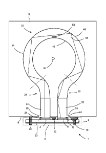
CA 2787221 2017-04-21
21
1 The
radiation guide has an inner wall 46 and an outer wall 48 perpendicular to the
plane
2 of the
sensor and opposing flats walls 50 and 52 parallel to the plane of the sensor.
One
3 more gas
access points 54 are provided within the inner wall to enable a gas sample to
4 diffuse
into the cavity 56 defined by the walls of the radiation guide from the
immediate
surroundings of the gas.sensor. The body of the sensor may comprise a dust
exclusion
6 grille
or fabric covered channel (not shown) for gas to diffuse from the surroundings
of
7 the gas sensor to the or each gas access point,
8 The
light emitting diode and photodiode are each formed from a narrow band gap Ill-
V
9 material
indium aluminium antimonide material ((lnl-x)AlxSb), grown on a gallium
arsenide (GaAs) substrate, the doping of which is chosen to tune the band gap
to cause
11 the
light emitting diode to emit light of a narrow wavelength range corresponding
to a
12
wavelength at which gaseous carbon dioxide absorbs strongly. The formation of
suitable
13 light
emitting diodes and photodiodes are disclosed in EP 0 864 180, EP 0 992 094,
and
14 in Haigh, M.K. et al., Applied Physics Letters. vol. 90, 231 116 (2007).
The light emitting diode and photodiode may be fabricated from the same
16
semiconducting substrate. The light emitting diode and photodiode may also be
17
fabricated from similar substrates and differ only in their epilayer
thicknesses, which
18 maybe
tuned to enhance the performance of light emission in the case of the light
19 emitting
diode or collection in the case of the photodiode. Due to their proximity and
the
present of heat conduction means, the light emitting diode and photodiode will
remain in
21 thermal
equilibrium, facilitating temperature compensation, for example, using a
22
temperature compensation circuit set out in WO 2009/019467 (Gas Sensing
Solutions
23 Limited).
24 In use,
the light emitting diode is driven by a conventional light emitting diode
driving
circuit. The light emitting diode emits electromagnetic radiation of a narrow
band of
26
wavelengths centred on 4.31J1n (in the case of a gas sensor for measuring
carbon
27 dioxide
concentration). The radiation is emitted with a broad angular spread and a
28
generally lambertian distribution. The radiation is partially collimated by
the collimator
29 and
passes through the first, second and third curved portions of the radiation
guide in
turn. All radiation will be reflected at least several times. Due to the
curvature in the
31 plane of the radiation guide. some radiation will be reflected onto a
path where it reflects
32 many times between the opposing walls and so is
CA 02787221 2012-07-16
WO 2011/086394 22
PCT/GB2011/050077
1
substantially attenuated, for example ray 58. However, radiation which
reflects off
2 the walls
which are generally parallel to the plane of the radiation guide will not
3 change the
component of its path in the plane of the radiation guide, avoiding the
4 additional
dispersion and attenuation which would arise if the walls which are
generally parallel to the plane of the radiation guide were not flat.
6
7 Much of the
radiation from the source will reflect several times off the walls which are
8 generally
parallel to the plane of the radiation guide. Thus, the mean path length
9 between the
light emitting diode and the photodiode is greater than would be the
case if the radiation from the light emitting diode was sufficiently
collimated to have
11 only a
narrow range of angles from the plane of the radiation guide. The condenser
12 typically
has the same profile as the collimator, except that it faces in the opposite
13 direction.
14
The radiation guide changes the mean direction of emitted radiation by 1800
between
16 the light
emitting diode and the detector, but the first curved portion curves by around
17 45 , the
second curved portion curves by around 270 in the opposite sense, and the
18 third curved
portion curves by around 45 in the same sense as the first curved
19 portion.
Thus, the integral of the magnitude of the curvature of the radiation guide
between the light emitting diode and the photodiode is around 360 . A
relatively long
21 gently
curved radiation guide has been provided, enabling a relatively long mean
22 path length to be achieved in a compact sensor.
23
24 Furthermore,
as a result of the configuration of the radiation guide, a substantial
proportion of radiation emitted by the light emitting diode will reach the
photodiode
26 provided
that it is not absorbed by gas. The amount of radiation detected by the
27 photodiode
will depend on the concentration of gas within the radiation guide which
28 absorbs radiation from the light emitting diode.
29
A gas sample enters and leaves the chamber within the radiation guide by
diffusion
31 through the
gas access port. The gas access port is located on the inside surface of
32 the second
curved portion. Less radiation is incident on the inside surface than the
33 outside
surface. Thus, less radiation is lost due to absorption or scattering by the
gas
34 access port
than would be the case if the gas access port was instead located on the
outside surface of the second curved portion. Several gas access ports can be
36 provided on
the inside surface of the second curved portion, and possible also other
37 curved
portions. As the sensor is relatively compact, the rate at which the
CA 02787221 2012-07-16
WO 2011/086394 23
PCT/GB2011/050077
1 composition
of gas within the radiation guide equilibrates with external gas (e.g. air) is
2 relatively
fast, providing a sensor with a relatively quick response to changing gas
3 concentrations.
4
The sensor may be operated without a reference signal. However, it is
preferable
6 that a
reference signal, which has only a low or no sensitivity to the concentration
of
7 analyte gas
is also measured, and used to calibrate the measurement signal, to
8 enable a more accurate measurement of analyte gas concentration to be
obtained.
9
Two examples of alternative apparatus and methods for obtaining a suitable
11 reference
signal will now be described. Each of these apparatus and methods may
12 be employed
with the apparatus described above and illustrated with reference to
13 Figures 1
through 5 and may also be employed with other types of optical absorption
14 gas sensor
having a radiation source and a detector sensitive to radiation from the
radiation source.
16
17 Example 1
18
19 With
reference to Figure 6, a first indium aluminium antimonide light emitting
diode
100, which emits radiation with a peak intensity at around 4.311m in use, is
provided
21 on a first
side 102 of a 1.6 mm thick fibreglass resin printed circuit board 104. The
22 first light
emitting diode is formed according to EP 0 864 180, EP 0 992 094, and in
23 Haigh, M.K.
et al., Applied Physics Letters, vol. 90, 231116 (2007). This first light
24 emitting
diode is driven by an electronic circuit 106, under control of a
microcontroller
108 to provide electromagnetic radiation which is detected by a photodiode
110. The
26 photodiode is
also based on indium aluminium antimonide and is mounted to a
27 printed
circuit board 112 which, when used with the gas sensor of Figures 1 to 5, is
28 preferably a
region of the printed circuit board to which the first light emitting diode is
29 mounted,
adjacent the light emitting diode, to facilitate thermal communication
between the light emitting diode and the photodiode through electronic
circuitry
31 printed on the printed circuit board.
32
33 The radiation
guide illustrated in Figures 1 though 5 extends between the light
34 emitting
diode and the photodiode, to direct radiation from the light emitting diode
through a sample gas so that the amount of radiation detected by the
photodiode is
36 sensitive to
the concentration of gas which absorbs radiation at around 4.3pm.
CA 02787221 2012-07-16
WO 2011/086394 24
PCT/GB2011/050077
1 Current from
the photodiode is amplified by a photodiode amplifier circuit 113 and the
2 resulting measurement is provided to the microcontroller.
3
4 The first
light emitting diode includes a bore 114 which extends through the circuit
board. A second light emitting diode 116, which emits electromagnetic
radiation at a
6 wavelength of
950 nm, is fixed to the opposite side of the circuit board to the first light
7 emitting
diode, and is oriented to direct emitted radiation through the bore. The first
8 light
emitting diode has an absorption spectrum illustrated in Figure 7. The first
light
9 emitting
diode transmits around 10% of radiation at a wavelength of 950 nm, and so
is translucent to radiation of this wavelength. Although the photodiode is
optimised to
11 detect
radiation of around 4.3 m wavelength, it is also sensitive to some extent to
12 radiation at
950 nm. Accordingly, radiation from the second light emitting diode can
13 also be
detected by the photodiode, and measured using the photodiode amplifier. A
14 second light
emitting diode drive circuit 118 is provided to drive the second light
emitting diode, under the control of the microcontroller.
16
17 In use, the
microcontroller signals the drive circuits for the first and second light
18 emitting
diodes so that the first and second light emitting diodes pulse alternately.
19 Thus, the
currents generated by the photodiode alternately provide a measure of
radiation received from the first and second light emitting diodes in turn.
Radiation at
21 from the
first light emitting diode, at a wavelength of around 4.3 m is absorbed in
22 dependence on
the amount of carbon dioxide which is present and the intensity
23 measured
while the first light emitting diode is illuminated provides a measurement
24 signal.
Radiation emitted at 950 nm by the second light emitting diode is only
absorbed minimally by carbon dioxide, and other gases typically found in the
26 atmosphere,
is low. Accordingly, the microcontroller can determine the concentration
27 of carbon
monoxide from the measurement signal while using the absorption of
28 radiation emitted by the second light emitting diode to calibrate the
measured signal.
29
Ideally, the second light emitting diode is chosen to have a similar response
to
31 temperature
and other environmental factors to the first light emitting diode. The path
32 for radiation
from the second light emitting diode to the photodiode is the same as the
33 path of a
radiation from the first light emitting diode to the photodiode, although the
34 angular
spread of radiation through the first light emitting diode from the second
light
emitting diode may be different to the angular spread of radiation generated
by the
36 first light
emitting diode. Nevertheless, this provides a useful calibration signal which
CA 02787221 2012-07-16
WO 2011/086394 25
PCT/GB2011/050077
1 can be
employed to provide a more accurate measured gas concentration signal than
2 would be possible using only a single light emitting diode.
3
4 In a
variation of this strategy, rather than being transmitted through the first
light
emitting radiation source, radiation from the second radiation source may be
reflected
6 around the
first radiation source, or a second radiation source may be provided which
7 extends
around the first radiation source. The first and second radiation sources are
8 controlled as before.
9
Example 2
11
12 In a second,
alternative approach for obtaining a reference measurement, we have
13 found that an
indium aluminium antimonide based photodiode will emit light when
14 driven using
a conventional light emitting diode driving circuit. Similarly, an indium
aluminium antimonide-based light emitting diode according to EP 0 864 180, EP
0
16 992 094, and
in Haigh, M.K. et al., Applied Physics Letters, vol. 90, 231116 (2007),
17 referred to
above, can be used as a photodiode by attachment to a conventional
18 photodiode amplifier circuit.
19
Thus, in the second example, a light emitting diode is pulsed, as before, and
the
21 current at
the photodiode is measured to provide a measurement signal. Between
22 each pulse of
the light emitting diode, the photodiode is driven to emit radiation, and
23 radiation
received at the light emitting diode is measured using an amplifier. In this
24 mode, the
radiation emitted by the photodiode is predominantly at a significantly
higher wavelength than the radiation emitted by the light emitting diode, and
is much
26 less
sensitive to carbon dioxide concentration. The emission spectra of the light
27 emitting diode 200 and the photodiode 202 are shown in Figures 8A and
8B.
28
29 Accordingly,
the current generated by the photodiode when the light emitting diode
emits radiation is used to derive a measurement signal and the current
generated by
31 the light
emitting diode while the photodiode emits radiation is used to derive a
32 reference
signal. A microcontroller uses the reference signal to calibrate the
33 measurement
signal and then outputs a signal which is a more accurate
34 measurement
of carbon dioxide concentration than would be possible without the
reference signal.
36
CA 02787221 2012-07-16
WO 2011/086394 26
PCT/GB2011/050077
1 One skilled in the art will appreciate that the two examples of apparatus
and methods
2 for obtaining a reference measurement may be employed in any optical
absorption
3 gas sensor and not only an optical absorption gas sensor according to
Figure 1 to 5.
4
Although the example optical absorption gas sensors disclosed herein are
adapted
6 for the detection of carbon dioxide, the sensors can be customised for
the detection
7 of different gaseous analytes by selecting radiation sources and
detectors adapted to
8 measure the attenuation of radiation having a wavelength or range of
wavelengths
9 corresponding to wavelengths at which the specific analytes absorb
strongly but at
which other components of air or potential interferents to do not absorb
strongly.
11
12 With reference to Figure 9, an alternative embodiment of the present
invention
13 provides a method of manufacture for optical absorption gas sensors
comprising a
14 cavity. The example embodiment of a linear rectangular radiation guide
will be used
to illustrate this method of manufacture.
16
17 A first L-shaped radiation guide portion 300 comprises a first 302 and a
second 304
18 elongate member having a major and minor dimension. The first elongate
member is
19 connected to the second elongate member along an edge along the major
dimension
306 to form a generally "L-shaped" radiation guide portion.
21
22 A second L-shaped radiation guide portion 308 comprises a first 310 and
a second
23 312 elongate member having a major and minor dimension. The first
elongate
24 member is connected to the second elongate member along an edge along
the major
dimension 314 to form a generally "L-shaped" radiation guide portion. The
first and
26 second radiation guide portions comprise an inner 316 and an outer
surface 318.
27
28 A gold layer is applied to the inner surface of the first and second L-
shaped radiation
29 guide portions by the process of sputtering, well known in the art. It
may be
necessary to apply a layer of chromium to the inner surface of the L-shaped
radiation
31 guide portions. A chromium layer enables the gold to bind strongly to
the L-shaped
32 radiation guide portions and may be necessary if the L-shaped radiation
guide
33 portions comprise a material with a low affinity for gold.
34
The first and second L-shaped radiation guide portions are arranged as
illustrated in
36 Figure 10A such that the first L-shaped radiation guide portion is anti-
aligned with the
37 second L-shaped radiation guide portion such that a cavity is formed
therebetween,
CA 02787221 2012-07-16
WO 2011/086394 27
PCT/GB2011/050077
1 and the gold
layer is on the interior surface of the hollow body so formed. The edges
2 of the first
and second L-shaped radiation guide portions are bonded together by
3 soldering. Alternatively they may be bonded by glue or welding, for
example.
4
In an alternative embodiment the gold layer may be replaced by an aluminium
layer
6 or two
dielectric layers. In the latter case, a layer of low refractive index, such
as ZnS
7 is applied
onto a layer of high refractive index, such as MgF2 or Ti02. Whilst an
8 extremely
effective reflective material, the application of two dielectric layers
requires
9 a high level of precision and is correspondingly expensive.
11 The above
method is in contrast the typical method of manufacture used for radiation
12 guides and
sample chambers, wherein a planar member 320 is bonded onto a
13 member
comprising a trench 322. A planar surface is straight forward to apply a
14 reflective
material to but a to apply a reflective material to the interior surface of a
trench is challenging if a smooth finish is to be obtained.
16
17 Further
variations and modifications may be made within the scope of the invention
18 herein disclosed.