Note: Descriptions are shown in the official language in which they were submitted.
CA 02788107 2012-07-24
WO 2011/097135 PCT/US2011/022986
LED-BASED RECTANGULAR ILLUMINATION DEVICE
CROSS REFERENCE TO RELATED APPLICATIONS
This application claims the benefit of Provisional
Application No. 61/301,546, filed February 4, 2010, and US
Serial No. 13/015,431, filed January 27, 2011, both of which are
incorporated by reference herein in their entirety.
TECHNICAL FIELD
The described embodiments relate to illumination devices
that include Light Emitting Diodes (LEDs).
BACKGROUND INFORMATION
The use of light emitting diodes in general lighting is
still limited due to limitations in light output level or flux
generated by the illumination devices due to the limited maximum
temperature of the LED chip, and the life time requirements,
which are strongly related to the temperature of the LED chip.
The temperature of the LED chip is determined by the cooling
capacity in the system, and the power efficiency of device
(optical power produced by the LEDs and LED system, versus the
electrical power going in). Illumination devices that use LEDs
also typically suffer from poor color quality characterized by
color point instability. The color point instability varies
over time as well as from part to part. Poor color quality is
also characterized by poor color rendering, which is due to the
spectrum produced by the LED light sources having bands with no
or little power. Further, illumination devices that use LEDs
typically have spatial and/or angular variations in the color.
Additionally, illumination devices that use LEDs are expensive
due to, among other things, the necessity of required color
control electronics and/or sensors to maintain the color point
of the light source or using only a selection of LEDs produced,
which meet the color and/or flux requirements for the
application.
1
CA 02788107 2012-07-24
WO 2011/097135 PCT/US2011/022986
Consequently, improvements to illumination device that
uses light emitting diodes as the light source are desired.
SUMMARY
An illumination device includes Light Emitting Diodes
(LEDs). In one embodiment, the illumination device includes a
light source sub-assembly having a length dimension extending in
a first direction, a width dimension extending in a second
direction perpendicular to the first direction, and a plurality
of Light Emitting Diodes (LEDs) mounted in a first plane,
wherein the width dimension is less than the length dimension.
A light conversion sub-assembly is mounted above the first plane
and physically separated from the plurality of LEDs and
configured to mix and color convert light emitted from the light
source sub-assembly. A first portion of a first interior
surface of the light conversion sub-assembly is aligned with the
first direction and is coated with a first type of wavelength
converting material and a first portion of a second interior
surface aligned with the second direction reflects incident
light without color conversion. A portion of an output window
of the light conversion sub-assembly is coated with a second
type of wavelength converting material. The first portion of
the second interior surface aligned with the second direction
and/or a bottom reflector insert may reflect at least 95% of
incident light between 380 nanometers and 780 nanometers without
color conversion.
In another embodiment, the illumination device includes a
mounting board having a length dimension extending in a first
direction, a width dimension extending in a second direction
perpendicular to the first direction, wherein the length
dimension is greater than the width dimension. A plurality of
LEDs is mounted to the mounting board. A light mixing cavity is
configured to reflect light emitted from the plurality of LEDs
until the light exits through an output window that is disposed
above the plurality of LEDs and is physically separated from the
plurality of LEDs. A first portion of the cavity, which is
2
CA 02788107 2012-07-24
WO 2011/097135 PCT/US2011/022986
aligned with the first direction, is coated with a first type of
wavelength converting material and a second portion of the
cavity, which is aligned with the second direction, reflects
incident light without color conversion. A portion of the
output window is coated with a second type of wavelength
converting material. The second portion of the second interior
surface aligned with the second direction and/or a bottom
reflector insert may reflect at least 95% of incident light
between 380 nanometers and 780 nanometers without color
conversion.
In another embodiment, the illumination device includes a
plurality of LEDs and a light mixing cavity mounted above and
physically separated from the plurality of LEDs and configured
to mix and color convert light emitted from the LEDs. A first
interior surface of the light mixing cavity includes a
replaceable, reflective insert that has a non-metallic, diffuse
reflective layer backed by a second reflective layer. The
second reflective layer may be specular reflective. The
replaceable, reflective insert may be a bottom reflector insert
that forms a bottom surface of the light mixing cavity and/or a
sidewall insert that forms sidewall surfaces of the light mixing
cavity.
In yet another embodiment, the illumination device
includes a mounting board having a plurality of raised pads and
a plurality of LEDs mounted on the raised pads of the mounting
board. A light mixing cavity is configured to reflect light
emitted from the plurality of LEDs until the light exits through
an output window. The light mixing cavity includes a bottom
reflector having a plurality of holes wherein the raised pads
elevate the LEDs above a top surface of the bottom reflector
through the holes. A first portion of the cavity is coated with
a first type of wavelength converting material and a portion of
the output window is coated with a second type of wavelength
converting material.
3
CA 02788107 2012-07-24
WO 2011/097135 PCT/US2011/022986
Further details and embodiments and techniques are
described in the detailed description below. This summary does
define the invention. The invention is defined by the claims.
BRIEF DESCRIPTION OF THE DRAWINGS
The accompanying drawings, where like numerals indicate
like components, illustrate embodiments of the invention.
Fig. 1 illustrates a perspective view of an embodiment of a
light emitting diode (LED) illumination device.
Fig. 2 shows an exploded view illustrating components of
the LED illumination device.
Figs. 3A and 3B illustrate perspective, cross-sectional
views of an embodiment of the LED illumination device.
Fig. 4 illustrates a mounting board that provides
electrical connections to the attached LEDs and a heat spreading
layer for the LED illumination device.
Fig. 5A illustrates a bottom reflector insert attached to
the top surface of the mounting board.
Fig. 5B illustrates a cross-sectional view of a portion of
the mounting board, a bottom reflector insert and an LED with a
submount, where the thickness of the bottom reflector insert is
approximately the same thickness as the submount of the LED.
Fig. 5C illustrates another cross-sectional view of a
portion of the mounting board, a bottom reflector insert and an
LED with a submount, where the thickness of bottom reflector
insert is significantly greater than the thickness of the
submount of the LED.
Fig. 5D illustrates another cross-sectional view of a
portion of the mounting board, a bottom reflector insert and an
LED with a submount, where the bottom reflector insert includes
a non-metallic layer and a thin metallic reflective backing
layer.
Fig. 5E illustrates a perspective view of another
embodiment of the mounting board and bottom reflector insert
that includes a raised portion between the LEDs.
4
CA 02788107 2012-07-24
WO 2011/097135 PCT/US2011/022986
Fig. 5F illustrates another embodiment of a bottom
reflector insert where each LED is surrounded by a separate
individual optical well.
Fig. 6A illustrates an embodiment of sidewall insert used
with the illumination device.
Figs. 6B and 6C illustrates a perspective view and side
view, respectively, of another embodiment of the sidewall insert
with a wavelength converting material patterned along the length
of the rectangular cavity and no wavelength converting material
patterned along the width.
Fig. 7A illustrates a side view of the output window for
the illumination device with a layer on the inside surface of
the window.
Fig. 7B illustrates a side view of another embodiment of
the output window for the illumination device with two
additional layers; one on the inside of the window and one on
the outside of the window.
Fig. 7C illustrates a side view of another embodiment of
the output window for the illumination device with two
additional layers; both on the same inside surface of the
window.
Fig. 8 shows a perspective view of a reflector mounted to
illumination device for collimating the light emitted from the
illumination device.
Fig. 9 illustrates illumination device with a bottom heat
sink attached.
Fig. 10 illustrates a side view of an illumination device
integrated into a retrofit lamp device.
DETAILED DESCRIPTION
Reference will now be made in detail to background examples
and some embodiments of the invention, examples of which are
illustrated in the accompanying drawings.
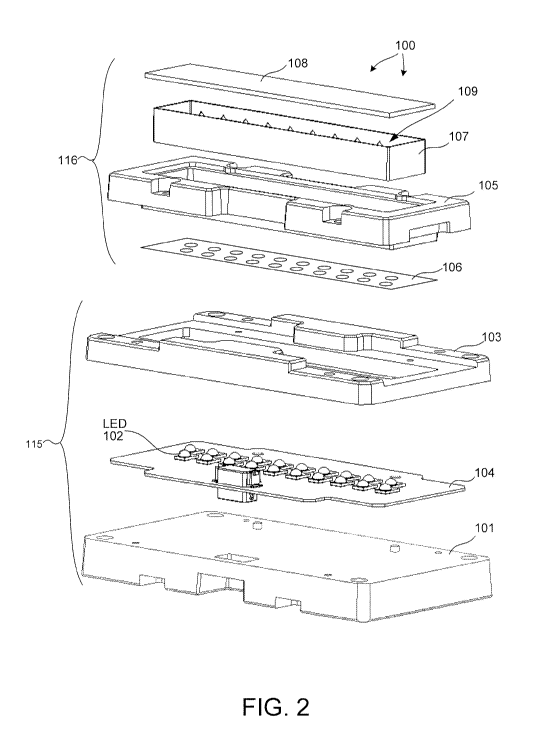
Fig. 1 illustrates a perspective view of an embodiment of a
light emitting diode (LED) illumination device 100. Fig. 2
5
CA 02788107 2012-07-24
WO 2011/097135 PCT/US2011/022986
shows an exploded view illustrating components of LED
illumination device 100. It should be understood that as
defined herein an LED illumination device is not an LED, but is
an LED light source or fixture or component part of an LED light
source or fixture. LED illumination device 100 includes one or
more LED die or packaged LEDs and a mounting board to which LED
die or packaged LEDs are attached. Figs. 3A and 3B illustrate
perspective, cross-sectional views of an embodiment of the LED
illumination device 100.
Referring to Fig. 2, LED illumination device 100 includes
one or more solid state light emitting elements, such as light
emitting diodes (LEDs) 102, mounted on mounting board 104.
Mounting board 104 is attached to mounting base 101 and secured
in position by mounting board retaining ring 103. Together,
mounting board 104 populated by LEDs 102 and mounting board
retaining ring 103 comprise light source sub-assembly 115.
Light source sub-assembly 115 is operable to convert electrical
energy into light using LEDs 102. The light emitted from light
source sub-assembly 115 is directed to light conversion sub-
assembly 116 for color mixing and color conversion. Light
conversion sub-assembly 116 includes cavity body 105 and output
window 108, and optionally includes either or both bottom
reflector insert 106 and sidewall insert 107. Output window 108
is fixed to the top of cavity body 105. Cavity body 105
includes interior sidewalls, which may be used to reflect light
from the LEDS 102 until the light exits through output window
108 when sub-assembly 116 is mounted over light source sub-
assembly 115. Bottom reflector insert 106 may optionally be
placed over mounting board 104. Bottom reflector insert 106
includes holes such that the light emitting portion of each LED
102 is not blocked by bottom reflector insert 106. Sidewall
insert 107 may optionally be placed inside cavity body 105 such
that the interior surfaces of sidewall insert 107 reflect the
light from the LEDS 102 until the light exits through output
6
CA 02788107 2012-07-24
WO 2011/097135 PCT/US2011/022986
window 108 when sub-assembly 116 is mounted over light source
sub-assembly 115.
In this embodiment, the sidewall insert 107, output window
108, and bottom reflector insert 106 disposed on mounting board
104 define a light mixing cavity 109 in the LED illumination
device 100 in which a portion of light from the LEDs 102 is
reflected until it exits through output window 108. Reflecting
the light within the cavity 109 prior to exiting the output
window 108 has the effect of mixing the light and providing a
more uniform distribution of the light that is emitted from the
LED illumination device 100.
Figs. 3A and 3B illustrate cut-away perspective views of
light mixing cavity 109. Portions of sidewall insert 107 may
including a coating 111 of wavelength converting material, such
as phosphor, as illustrated in Figs. 3A and 3B. Furthermore,
portions of output window 108 may be coated with a different
wavelength converting material (shown in Fig. 7B). The photo
converting properties of these materials in combination with the
mixing of light within cavity 109 results in a color converted
light output by output window 108. By tuning the chemical
properties of the wavelength converting materials and the
geometric properties of the coatings on the interior surfaces of
cavity 109, specific color properties of light output by output
window 108 may be specified, e.g. color point, color
temperature, and color rendering index (CRI).
Cavity 109 may be filled with a non-solid material, such as
air or an inert gas, so that the LEDs 102 emit light into the
non-solid material as opposed to into a solid encapsulent
material. By way of example, the cavity may be hermetically
sealed and Argon gas used to fill the cavity. Alternatively,
Nitrogen may be used.
The LEDs 102 can emit light having different or the same
colors, either by direct emission or by phosphor conversion,
e.g., where phosphor layers are applied to the LEDs as part of
the LED package. Thus, the illumination device 100 may use any
7
CA 02788107 2012-07-24
WO 2011/097135 PCT/US2011/022986
combination of colored LEDs 102, such as red, green, blue,
amber, or cyan, or the LEDs 102 may all produce the same color
light or may all produce white light. For example, the LEDs 102
may all emit either blue or UV light. In addition, the LEDs 102
may emit polarized light or non-polarized light and LED based
illumination device 100 may use any combination of polarized or
non-polarized LEDs. When used in combination with phosphors (or
other wavelength conversion means such as luminescent dyes),
which may be, e.g., in or on the output window 108, applied to
the sidewalls of cavity body 105, or applied to other components
placed inside the cavity (such as sidewall insert 107 and/or
bottom reflector insert 106 or other inserted components not
shown), the output light of the illumination device 100 has the
color as desired. The phosphors may be chosen from the set
denoted by the following chemical formulas: Y3Al5O12:Ce, (also
known as YAG:Ce, or simply YAG) (Y,Gd)3Al5012:Ce, CaS:Eu, SrS:Eu,
SrGa2S4:E u, Ca3(Sc,Mg)2Si3O12:Ce, Ca3Sc2Si3O12:Ce, Ca3Sc2O4:Ce,
Ba3Si6012N2 : Eu, (Sr, Ca) A1SiN3 : Eu, CaA1SiN3 : Eu, CaAlSi (ON) 3 : Eu,
Ba2Si04 : Eu, Sr2Si04 : Eu, Ca2SiO4: Eu, CaSc204 : Ce, CaSi202N2 : Eu,
SrSi202N2 : Eu, BaSi202N2 : Eu, Ca5 (P04) 3C1 : Eu, Ba5 (P04) 3C1 : Eu,
Cs2CaP2O7, Cs2SrP2O7, Lu3A15012 : Ce, Ca8Mg (Si04) 4012 : Eu,
Sr8Mg(Si04)4Cl2:Eu, La3Si6N11:Ce, Y3Ga5O12:Ce, Gd3Ga5O12:Ce,
Tb3A15O12 : Ce, Tb3Ga5O12 : Ce, and Lu3Ga5O12 : Ce . The adjustment of
color point of the illumination device may be accomplished by
replacing sidewall insert 107 and/or the output window 108,
which similarly may be coated or impregnated with one or more
wavelength converting materials, and are selected based on their
performance, such as their color conversion properties.
In one embodiment a red emitting phosphor such as
CaAlSiN3:Eu, or (Sr,Ca)AlSiN3:Eu covers a portion of sidewall
insert 107 and bottom reflector insert 106 at the bottom of the
cavity 109, and a YAG phosphor covers a portion of the output
window 108. By choosing the shape and height of the sidewalls
that define the cavity, and selecting which of the parts in the
cavity will be covered with phosphor or not, and by optimization
8
CA 02788107 2012-07-24
WO 2011/097135 PCT/US2011/022986
of the layer thickness of the phosphor layer on the window, the
color point of the light emitted from the module can be tuned as
desired.
In one example, a single type of wavelength converting
material may be patterned on the sidewall, which may be, e.g.,
the sidewall insert 107 shown in Fig. 3B. By way of example, a
red phosphor may be patterned on different areas of the sidewall
insert 107 and a yellow phosphor may cover the output window
108, shown in Fig. 7A. The coverage and/or concentrations of
the phosphors may be varied to produce different color
temperatures. It should be understood that the coverage area of
the red and/or the concentrations of the red and yellow
phosphors will need to vary to produce the desired color
temperatures if the blue light produced by the LEDs 102 varies.
The color performance of the LEDs 102, red phosphor on the
sidewall insert 107 and the yellow phosphor on the output window
108 may be measured before assembly and selected based on
performance so that the assembled pieces produce the desired
color temperature. In one example, the thickness of the red
phosphor may be, e.g., between 60 m to 100 m and more
specifically between 80 m to 90 m, while the thickness of the
yellow phosphor may be, e.g., between 100 m to 140 m and more
specifically between 110 m to 120 m. The red phosphor may be
mixed with a binder at a concentration of 1%-3% by volume. The
yellow phosphor may be mixed with a binder at a concentration of
12%-17% by volume.
Fig. 4 illustrates mounting board 104 in greater detail.
The mounting board 104 provides electrical connections to the
attached LEDs 102 to a power supply (not shown). In one
embodiment, the LEDs 102 are packaged LEDs, such as the Luxeon
Rebel manufactured by Philips Lumileds Lighting. Other types of
packaged LEDs may also be used, such as those manufactured by
OSRAM (Ostar package), Luminus Devices (USA), Cree (USA), Nichia
(Japan), or Tridonic (Austria). As defined herein, a packaged
9
CA 02788107 2012-07-24
WO 2011/097135 PCT/US2011/022986
LED is an assembly of one or more LED die that contains
electrical connections, such as wire bond connections or stud
bumps, and possibly includes an optical element and thermal,
mechanical, and electrical interfaces. The LEDs 102 may include
a lens over the LED chips. Alternatively, LEDs without a lens
may be used. LEDs without lenses may include protective layers,
which may include phosphors. The phosphors can be applied as a
dispersion in a binder, or applied as a separate plate. Each
LED 102 includes at least one LED chip or die, which may be
mounted on a submount. The LED chip typically has a size about
lmm by lmm by 0.5mm, but these dimensions may vary. In some
embodiments, the LEDs 102 may include multiple chips. The
multiple chips can emit light of similar or different colors,
e.g., red, green, and blue. In addition, different phosphor
layers may be applied on different chips on the same submount.
The submount may be ceramic or other appropriate material. The
submount typically includes electrical contact pads on a bottom
surface that are coupled to contacts on the mounting board 104.
Alternatively, electrical bond wires may be used to electrically
connect the chips to a mounting board. Along with electrical
contact pads, the LEDs 102 may include thermal contact areas on
the bottom surface of the submount through which heat generated
by the LED chips can be extracted. The thermal contact areas of
the LEDs are coupled to heat spreading layers 131 on the
mounting board 104. Heat spreading layers 131 may be disposed
on any of the top, bottom, or intermediate layers of mounting
board 104. Heat spreading layers 131 may be connected by vias
that connect any of the top, bottom, and intermediate heat
spreading layers.
In some embodiments, the mounting board 104 conducts heat
generated by the LEDs 102 to the sides of the board 104 and the
bottom of the board 104. In one example, the bottom of mounting
board 104 may be thermally coupled to a heat sink 130 (shown in
Fig. 9) via mounting base 101. In other examples, mounting
board 104 may be directly coupled to a heat sink, or a lighting
CA 02788107 2012-07-24
WO 2011/097135 PCT/US2011/022986
fixture and/or other mechanisms to dissipate the heat, such as a
fan. In some embodiments, the mounting board 104 conducts heat
to a heat sink thermally coupled to the top of the board 104.
For example, mounting board retaining ring 103 and cavity body
105 may conduct heat away from the top surface of mounting board
104. Mounting board 104 may be an FR4 board, e.g., that is
0.5mm thick, with relatively thick copper layers, e.g., 30 m to
100 m, on the top and bottom surfaces that serve as thermal
contact areas. In other examples, the board 104 may be a metal
core printed circuit board (PCB) or a ceramic submount with
appropriate electrical connections. Other types of boards may
be used, such as those made of alumina (aluminum oxide in
ceramic form), or aluminum nitride (also in ceramic form).
Mounting board 104 includes electrical pads to which the
electrical pads on the LEDs 102 are connected. The electrical
pads are electrically connected by a metal, e.g., copper, trace
to a contact, to which a wire, bridge or other external
electrical source is connected. In some embodiments, the
electrical pads may be vias through the board 104 and the
electrical connection is made on the opposite side, i.e., the
bottom, of the board. Mounting board 104, as illustrated, is
rectangular in dimension. LEDs 102 mounted to mounting board
104 may be arranged in different configurations on rectangular
mounting board 104. In one example LEDs 102 are aligned in rows
extending in the length dimension and in columns extending in
the width dimension of mounting board 104. In another example,
LEDs 102 have a hexagonal arrangement to produce a closely
packed structure. In such an arrangement each LED is
equidistant from each of its immediate neighbors. Such an
arrangement is desirable to increase the uniformity of light
emitted from the light source sub-assembly 115.
Fig. 5A illustrates a bottom reflector insert 106 attached
to the top surface of the mounting board 104. The bottom
reflector insert 106 may be made from a material with high
thermal conductivity and may be placed in thermal contact with
11
CA 02788107 2012-07-24
WO 2011/097135 PCT/US2011/022986
the board 104. As illustrated, the bottom reflector insert 106
may be mounted on the top surface of the board 104, around the
LEDs 102. The bottom reflector insert 106 may be highly
reflective so that light reflecting downward in the cavity 109
is reflected back generally towards the output window 108. The
bottom reflector insert, by way of example, may reflect at least
95% of incident light between 380 nanometers and 780 nanometers.
Additionally, the bottom reflector insert 106 may have a high
thermal conductivity, such that it acts as an additional heat
spreader.
As illustrated in Fig. 5B, the thickness of the bottom
reflector insert 106 may be approximately the same thickness as
the submounts 102submount of the LEDs 102 or slightly thicker.
Holes are punched in the bottom reflector insert 106 for the
LEDs 102 and bottom reflector insert 106 is mounted over the LED
package submounts 102submount, and the rest of the board 104. In
this manner a highly reflective surface covers the bottom of
cavity body 105 except in the areas where light is emitted by
LEDs 102. By way of example, the bottom reflector insert 106
may be made with a highly thermally conductive material, such as
an aluminum based material that is processed to make the
material highly reflective and durable. By way of example, a
material referred to as Miro , manufactured by Alanod, a German
company, may be used as the bottom reflector insert 106. The
high reflectivity of the bottom reflector insert 106 may either
be achieved by polishing the aluminum, or by covering the inside
surface of the bottom reflector insert 106 with one or more
reflective coatings. The bottom reflector insert 106 might
alternatively be made from a highly reflective thin material,
such as VikuitiT"' ESR, as sold by 3M (USA), which has a thickness
of 65 m.
In other examples, bottom reflector insert 106 may be made
from a highly reflective non-metallic material such as LumirrorTM
E60L manufactured by Toray (Japan) or microcrystalline
polyethylene terephthalate (MCPET) such as that manufactured by
12
CA 02788107 2012-07-24
WO 2011/097135 PCT/US2011/022986
Furukawa Electric Co. Ltd. (Japan) or a sintered PTFE material
such as that manufactured by W.L. Gore (USA). The thickness of
bottom reflector insert 106, particularly when constructed from
a non-metallic reflective film, may be significantly greater
than the thickness of the submounts 102submount of LEDs 102 as
illustrated in Fig. 5C. To accommodate for the increased
thickness without impinging on light emitted from LEDs 102,
holes may be punched in the bottom reflector insert 106 to
reveal the submount 102submount of the LED package, and bottom
reflector insert 106 is mounted directly on top of mounting
board 104. In this manner, the thickness of bottom reflector
insert 106 may be greater than the thickness of the submount
102submount without significantly impinging on light emitted by
LEDs 102. This solution is particularly attractive when LED
packages with submounts that are only slightly larger than the
light emitting portion of the LED are employed. In other
examples, mounting board 104 may include raised pads 104pad to
approximately match the footprint of the LED submount 102submount
such that the light emitting portion of LED 102 is raised above
bottom reflector insert 106. In some examples, the non-metallic
layer 106a may be backed by a thin metallic reflective backing
layer 106b to enhance overall reflectivity as illustrated in
Fig. 5D. For example, the non-metallic reflective layer 106a
may exhibit diffuse reflective properties and the reflective
backing layer 106b may exhibit specular reflective properties.
This approach has been effective in reducing the potential for
wave-guiding inside specular reflective layers. It is desirable
to minimize wave-guiding within reflective layers because wave-
guiding reduces overall cavity efficiency.
The cavity body 105 and the bottom reflector insert 106 may
be thermally coupled and may be produced as one piece if
desired. The bottom reflector insert 106 may be mounted to the
board 104, e.g., using a thermal conductive paste or tape. In
another embodiment, the top surface of the mounting board 104 is
configured to be highly reflective, so as to obviate the need
13
CA 02788107 2012-07-24
WO 2011/097135 PCT/US2011/022986
for the bottom reflector insert 106. Alternatively, a
reflective coating might be applied to board 104, the coating
composed of white particles e.g. made from Ti02, ZnO, or BaSO4
immersed in a transparent binder such as an epoxy, silicone,
acrylic, or N-Methylpyrrolidone (NMP) materials. Alternatively,
the coating might be made from a phosphor material such as
YAG:Ce. The coating of phosphor material and/or the Ti02, ZnO
or GaSO4 material may be applied directly to the board 104 or
to, e.g., the bottom reflector insert 106, for example, by
screen printing.
Fig. 5E illustrates a perspective view of another
embodiment of illumination device 100. If desired, e.g., where
a large number of LEDs 102 are used, the bottom reflector insert
106 may include a raised portion between the LEDs 102 such as
that illustrated in Fig. 5D. Illumination device 100 is
illustrated in Fig. 5D with a diverter 117 between the LEDs
configured to redirect light emitted at large angles from the
LEDs 102 into narrower angles with respect to a normal to the
top surface of mounting board 104. In this manner, light
emitted by LEDs 102 that is close to parallel to the top surface
of mounting board 104 is redirected upwards toward the output
window 108 so that the light emitted by the illumination device
has a smaller cone angle compared to the cone angle of the light
emitted by the LEDs directly. The use of a bottom reflector
insert 106 with a diverter 117 is useful when LEDs 102 are
selected that emit light over large output angles, such as LEDs
that approximate a Lambertian source. By reflecting the light
into narrower angles, the illumination device 100 can be used in
applications where light under large angles is to be avoided,
for example, due to glare issues (office lighting or general
lighting), or due to efficiency reasons where it is desirable to
send light only where it is needed and most effective, e.g. task
lighting and under cabinet lighting. Moreover, the efficiency
of light extraction is improved for the illumination device 100
as light emitted in large angles undergoes fewer reflections in
14
CA 02788107 2012-07-24
WO 2011/097135 PCT/US2011/022986
cavity 109 before reaching the output window 108 compared to a
device without the bottom reflector insert 106. This is
particularly advantageous when used in combination with a light
tunnel or integrator, as it is beneficial to limit the flux in
large angles due to efficiency losses incurred by repeated
reflections in the mixing cavity. The diverter 117 is
illustrated as having a tapered shape, but alternative shapes
may be used if desired, for example, a half dome shape, or a
spherical cap, or aspherical reflector shapes. The diverter 117
can have a specular reflective coating, a diffuse coating, or
can be coated with one or more phosphors. The height of the
diverter 117 may be smaller than the height of the cavity 109
(e.g., approximately half the height of the cavity 109) so that
there is a small space between the top of the diverter 117, and
the output window 108. There may be multiple diverters
implemented in cavity 109.
Fig. 5F illustrates another embodiment of a bottom
reflector insert 106 where each LED 102 in illumination device
100 is surrounded by a separate individual optical well 118.
Optical well 118 may have a parabolic, compound parabolic,
elliptical shape, or other appropriate shape. The light from
illumination device 100 is collimated from large angles into
smaller angles, e.g., from a 2 x 90 degree angle to a 2 x 60
degree angle, or a 2 x 45 degree beam. The illumination device
100 can be used as a direct light source, for example, as a down
light or an under the cabinet light, or it can be used to inject
the light into a cavity 109. The optical well 118 can have a
specular reflective coating, a diffuse coating, or can be coated
with one or more phosphors. Optical well 118 may be constructed
as part of bottom reflector insert 106 in one piece of material
or may be constructed separately and combined with bottom
reflector insert 106 to form a bottom reflector insert 106 with
optical well features.
Fig. 6A illustrates sidewall insert 107. Sidewall insert
107 may be made with highly thermally conductive material, such
CA 02788107 2012-07-24
WO 2011/097135 PCT/US2011/022986
as an aluminum based material that is processed to make the
material highly reflective and durable. By way of example, a
material referred to as Miro , manufactured by Alanod, a German
company, may be used. The high reflectivity of sidewall insert
107 may be achieved by polishing the aluminum, or by covering
the inside surface of the sidewall insert 107 with one or more
reflective coatings. The bottom reflector insert 106 might
alternatively be made from a highly reflective thin material,
such as VikuitiT"' ESR, as sold by 3M (USA), which has a thickness
of 65 m. In other examples, bottom reflector insert 106 may be
made from a highly reflective non-metallic material such as
LumirrorTM E60L manufactured by Toray (Japan) or microcrystalline
polyethylene terephthalate (MCPET) such as that manufactured by
Furukawa Electric Co. Ltd. (Japan) or a sintered PTFE material
such as that manufactured by W.L. Gore (USA). The interior
surfaces of sidewall insert 107 can either be specular
reflective or diffuse reflective. An example of a highly
specular reflective coating is a silver mirror, with a
transparent layer protecting the silver layer from oxidation.
Examples of highly diffuse reflective materials include MCPET,
PTFE, and Toray E60L materials. Also, highly diffuse reflective
coatings can be applied. Such coatings may include titanium
dioxide (Ti02), zinc oxide (ZnO), and barium sulfate (BaS04)
particles, or a combination of these materials.
In other examples, a non-metallic reflective layer may be
backed by a reflective backing layer to enhance overall
reflectivity. For example, the non-metallic reflective layer
may exhibit diffuse reflective properties and the reflective
backing layer may exhibit specular reflective properties. This
approach has been effective in reducing the potential for wave-
guiding inside specular reflective layers; resulting in
increased cavity efficiency.
In one embodiment, sidewall insert 107 may be made of a
highly diffuse, reflective MCPET material. A portion of the
interior surfaces may be coated with an overcoat layer or
16
CA 02788107 2012-07-24
WO 2011/097135 PCT/US2011/022986
impregnated with a wavelength converting material, such as
phosphor or luminescent dyes. Such a wavelength converting
material will be generally referred to herein as phosphor for
the sake of simplicity, although any photoluminescent material,
or combination of photoluminescent materials, is considered a
wavelength converting material for purposes of this patent
document. By way of example, a phosphor that may be used may
include Y3A15012 : Ce, (Y, Gd) 3A15012 : Ce, CaS : Eu, SrS : Eu, SrGa2S4 : Eu,
Ca3(Sc,Mg)2Si3O12:Ce, Ca3Sc2Si3O12:Ce, Ca3Sc204:Ce, B a3Si6O12N2:Eu,
(Sr,Ca)AlSiN3:Eu, CaAlSiN3:Eu, CaAlSi(ON)3:Eu, Ba2SiO4:Eu,
Sr2SiO4 : Eu, Ca2SiO4 : Eu, CaSc204: Ce, CaSi202N2 : Eu, SrSi202N2 : Eu,
BaSi202N2 : Eu, Ca5 (P04) 3C1 : Eu, Ba5 (P04) 3C1 : Eu, Cs2CaP2O7, Cs2SrP2O7,
Lu3A15O12 : Ce, Ca8Mg (5i04) 4012 : Eu, Sr8Mg (5i04) 4012 : Eu, La3Si6N11 :
Ce,
Y3Ga5O12:Ce, Gd3Ga5O12:Ce, Tb3Al5O12:Ce, Tb3Ga5O12:Ce, and
Lu3Ga5O12 : Ce.
As discussed above, the interior sidewall surfaces of
cavity 109 may be realized using a separate sidewall insert 107
that is placed inside cavity body 105, or may be achieved by
treatment of the interior surfaces of cavity body 105. Sidewall
insert 107 may be positioned within cavity body 105 and used to
define the sidewalls of cavity 109. By way of example, sidewall
insert 107 can be inserted into cavity body 105 from the top or
the bottom depending on which side has a larger opening.
Figs. 6B-6C illustrate treatment of selected interior
sidewall surfaces of cavity 109. As illustrated in Figs. 6B and
6C, the described treatments are applied to sidewall insert 107,
but as discussed above, sidewall insert 107 may not be used and
the described treatments may be applied to the interior surfaces
of cavity body 105 directly. Fig. 6b illustrates a rectangular
cavity having a length extending along the longer dimension
pictured and a width extending along the shorter dimension
pictured. In this example, a reflective coating 113 is applied
to the two shorter sidewall surfaces 107s and a coating 111 of
wavelength converting material is applied along the sidewall
surfaces 1071 corresponding with the length dimension. If
17
CA 02788107 2012-07-24
WO 2011/097135 PCT/US2011/022986
desired, the material used to form the sidewall insert 107
itself may be reflective, thereby obviating the need for
reflective coating 113. In one embodiment, the shorter sidewall
surfaces 107s reflect at least 95% of incident light between 380
nanometers and 780 nanometers without color conversion. This
combination of treatments to sidewall insert 107, i.e.,
reflective short sidewall surfaces 107s and wavelength
converting long sidewalls surfaces 1071, has been found to be
particularly advantageous. The implementation of a reflective
surface on the sidewall surfaces 107s corresponding to the width
dimension has proven to improve the color uniformity of the
output beam emitted from output window 108. Figs. 6B and 6C
illustrate a sawtooth shaped patterned coating 111 where the
peak of each sawtooth is aligned with the placement of each LED
102 as illustrated in Fig. 6C. Any portion of the sidewall
surfaces 1071 without coating 111 are reflective and, e.g., may
reflect at least 95% of incident light between 380 nanometers
and 780 nanometers without color conversion. The implementation
of phosphor patterns on the sidewall surfaces 1071 corresponding
to the length dimension where the phosphor pattern is
concentrated around the LEDs has also improved color uniformity
and enables more efficient use of phosphor materials. Although,
a sawtooth pattern is illustrated, other patterns such as
semicircular, parabolic, flattened sawtooth patterns, and others
may be employed to similar effect. Moreover, if desired, the
coating 111 may have no pattern, i.e., the entirety of the
sidewall surfaces 1071 may be coated with phosphor.
Figs. 7A-7C illustrate various configurations of output
window 108 in cross sectional views. In Figs. 3A and 3B, the
window 108 is shown mounted on top of the cavity body 105. It
can be beneficial to seal the gap between the window 108 and the
cavity body 105 to form a hermetically sealed cavity 109, such
that no dust or humidity can enter the cavity 109. A sealing
material may be used to fill the gap between the window 108 and
the cavity body 105, as for example an epoxy or a silicone
18
CA 02788107 2012-07-24
WO 2011/097135 PCT/US2011/022986
material. It may be beneficial to use a material that remains
flexible over time due to the differences in thermal expansion
coefficients of the materials of the window 108 and cavity body
105. As an alternative, the window 108 might be made of glass
or a transparent ceramic material, and soldered onto the cavity
body 105. In that case, the window 108 may be plated at the
edges with a metallic material, such as aluminum, or silver, or
copper, or gold, and solder paste is applied in between the
cavity body 105 and window 108. By heating the window 108 and
the cavity body 105, the solder will melt and provide a good
connection between the cavity body 105 and window 108.
In Fig. 7A, the window 108 has an additional layer 124 on
the inside surface of the window, i.e., the surface facing the
cavity 109. The additional layer 124 may contain either or both
diffusing particles and particles with wavelength converting
properties such as phosphors. The layer 124 can be applied to
the window 108 by screen printing, spray painting, or powder
coating. For screen printing and spray painting, typically the
particles are immersed in a binder, which can by a polyurethane
based lacquer, or a silicone material. For powder coating a
binding material is mixed into the powder mix in the form of
small pellets which have a low melting point, and which make a
uniform layer when the window 108 is heated, or a base coat is
applied to the window 108 to which the particles stick during
the coating process. Alternatively, the powder coating may be
applied using an electric field, and the window and phosphor
particles baked in an oven so that the phosphor permanently
adheres to the window. The thickness and optical properties of
the layer 124 applied to the window 108 may be monitored during
the powder coat process for example by using a laser and a
spectrometer, and/or detector, or and/or camera, both in forward
scatter and back scattered modes, to obtain the right color
and/or optical properties.
In Fig. 7B the window 108 has two additional layers 124 and
126; one on the inside of the window and one on the outside of
19
CA 02788107 2012-07-24
WO 2011/097135 PCT/US2011/022986
the window 108, respectively. The outside layer 126 may be
light scattering particles, such as Ti02, ZnO, and/or BaSO4
particles. Phosphor particles may be added to the layer 126 to
do a final adjustment of the color of the light coming out of
the illumination device 100. The inside layer 124 may contain
wavelength converting particles, such as a phosphor.
In Fig. 7C the window 108 also has two additional layers
124 and 128, but both are on the same inside surface of the
window 108. While two layers are shown, it should be understood
that additional layers may be used. In one configuration, layer
124, which is closest to the window 108, includes white
scattering particles, such that the window 108 appears white if
viewed from the outside, and has a uniform light output over
angle, and layer 128 includes a yellow emitting phosphor.
The phosphor conversion process generates heat and thus the
window 108 and the phosphor, e.g., in layer 124, on the window
108, should be configured so that they do not get too hot. For
this purpose, the window 108 may have a high thermal
conductivity, e.g., not less than 1W/(m K), and the window 108
may be thermally coupled to the cavity body 105, which serves as
a heat-sink, using a material with low thermal resistance, such
as solder, thermal paste or thermal tape. A good material for
the window is aluminum oxide, which can be used in its
crystalline form, called Sapphire, as well in its poly-
crystalline or ceramic form, called Alumina. Other patterns may
be used if desired as for example small dots with varying size,
thickness and density.
Fig. 8 shows a perspective view of a reflector 140 mounted
to illumination device 100 for collimating the light emitted
from the cavity 109. The reflector 140 may be made out of a
thermal conductive material, such as a material that includes
aluminum or copper and may be thermally coupled to a heat
spreader on the board 104, as discussed in reference to Fig. 4A,
along with or through cavity body 105. Heat flows by conduction
through heat spreading layers 131 attached to board 104, the
CA 02788107 2012-07-24
WO 2011/097135 PCT/US2011/022986
thermally conductive cavity body 105, and the thermally
conductive reflector 140. Heat also flows via thermal
convection over the reflector 140. Reflector 140 may be a
compound parabolic concentrator, where the concentrator is made
out of a highly reflecting material. Compound parabolic
concentrators tend to be tall, but they often are used in a
reduced length form, which increases the beam angle. An
advantage of this configuration is that no additional diffusers
are required to homogenize the light, which increases the
throughput efficiency. Optical elements, such as a diffuser or
reflector 140 may be removably coupled to the cavity body 105,
e.g., by means of threads, a clamp, a twist-lock mechanism, or
other appropriate arrangement. In other examples, diffuser or
reflector 140 may be coupled to mounting base 101 directly.
Fig. 9 illustrates illumination device 100 with a bottom
heat sink 130 attached. In one embodiment, the board 104 may be
bonded to the heat sink 130 by way of thermal epoxy.
Alternatively or additionally, the heat sink 130 may be screwed
to the illumination device 100, via screw threads to clamp the
illumination device 100 to the heat sink 130, as illustrated in
Fig. 9. As can be seen in Fig. 4, the board 104 may include
heat spreading layers 131 that act as thermal contact areas that
are thermally coupled to heat sink 130, e.g., using thermal
grease, thermal tape or thermal epoxy. For adequate cooling of
the LEDs, a thermal contact area of at least 50 square
millimeters, but preferably 100 square millimeters should be
used per one watt of electrical energy flow into the LEDs on the
board. For example, in the case when 20 LEDs are used, a 1000
to 2000 square millimeter heatsink contact area should be used.
Using a larger heat sink 130 permits the LEDs 102 to be driven
at higher power, and also allows for different heat sink
designs, so that the cooling capacity is less dependent on the
orientation of the heat sink. In addition, fans or other
solutions for forced cooling may be used to remove the heat from
21
CA 02788107 2012-07-24
WO 2011/097135 PCT/US2011/022986
the device. The bottom heat sink may include an aperture so
that electrical connections can be made to the board 104.
Heat spreading layer 131 on the board 104, shown in e.g.,
Fig. 4, may be attached to either the reflector, or to a heat
sink, such as heat sink 130. In addition, heat spreading layer
131 may be attached directly to an external structure such as a
light fixture. In other embodiments, reflector 140 may be made
of a metal such as aluminum, copper or alloys thereof, and is
thermally coupled to the heat sink 130 to assist in heat
dissipation.
As illustrated in Figs. 1 and 2, multiple LEDs 102 may be
used in the illumination device 100. The LEDs 102 are
positioned linearly along the length and width dimension shown.
The illumination device 100 may have more or fewer LEDs, but
twenty LEDs has been found to be a useful quantity of LEDs 102.
In one embodiment, twenty LEDs are used. When a large number of
LEDs is used, it may be desirable to combine the LEDs into
multiple strings, e.g., two strings of ten LEDs, in order to
maintain a relatively low forward voltage and current, e.g., no
more than 24V and 700mA. If desired, a larger number of the
LEDs may be placed in series, but such a configuration may lead
to electrical safety issues.
Any of sidewall insert 107, bottom reflector insert 106,
and output window 108 may be patterned with phosphor. Both the
pattern itself and the phosphor composition may vary. In one
embodiment, the illumination device may include different types
of phosphors that are located at different areas of the light
mixing cavity 109. For example, a red phosphor may be located
on either or both of the sidewall insert 107 and the bottom
reflector insert 106 and yellow and green phosphors may be
located on the top or bottom surfaces of the window 108 or
embedded within the window 108. In one embodiment, a central
reflector, e.g., such as diverter 117 shown in Fig. 5E, may have
patterns of different types of phosphor, e.g., a red phosphor on
a first area and a green phosphor on a separate second area. In
22
CA 02788107 2012-07-24
WO 2011/097135 PCT/US2011/022986
another embodiment, different types of phosphors, e.g., red and
green, may be located on different areas on the sidewalls of the
sidewall insert 107 or the cavity body 105. For example, one
type of phosphor may be patterned on the sidewall insert 107 at
a first area, e.g., in stripes, spots, or other patterns, while
another type of phosphor is located on a different second area
of the sidewall insert 107. If desired, additional phosphors
may be used and located in different areas in the cavity 109.
Additionally, if desired, only a single type of wavelength
converting material may be used and patterned in the cavity 109,
e.g., on the sidewalls.
The luminaire illustrated in Fig. 10 includes an
illumination device 100 integrated into a retrofit lamp device
150. The retrofit lamp device 150 includes a reflector 140 with
an internal surface 142 that is polished to be reflective or
optionally includes a reflective coating and/or a wavelength
converting layer. The reflector 140 may further include a
window 144 that may optionally include a coating of a wavelength
converting layer or other optical coating such as a dichroic
filter. It should be understood that as defined herein an LED
based illumination device is not an LED, but is an LED light
source or fixture or component part of an LED light source or
fixture. In some embodiments, LED based illumination device 100
may be a replacement lamp or retrofit lamp or a part of a
replacement lamp or retrofit lamp. As illustrated in Fig. 10,
an LED based illumination device 100 may be a part of an LED
based retrofit lamp device 150.
Although certain specific embodiments are described above
for instructional purposes, the teachings of this patent
document have general applicability and are not limited to the
specific embodiments described above. For example, Figs. 3A and
3B illustrate the side walls as having a linear configuration,
but it should understood that the sidewalls may have any desired
configuration, e.g., curved, non-vertical, beveled etc. For
example, a higher transfer efficiency is achieved through the
23
CA 02788107 2012-07-24
WO 2011/097135 PCT/US2011/022986
light mixing cavity 109 by pre-collimation of the light using
tapered side walls. In another example, cavity body 105 is used
to clamp mounting board 104 directly to mounting base 101
without the use of mounting board retaining ring 103. In other
examples mounting base 101 and heat sink 130 may be a single
component. The examples illustrated in Figs. 8-10 are for
illustrative purposes. Examples of illumination devices of
general polygonal and elliptical shapes may also be
contemplated. Accordingly, various modifications, adaptations,
and combinations of various features of the described
embodiments can be practiced without departing from the scope of
the invention as set forth in the claims.
24