Note: Descriptions are shown in the official language in which they were submitted.
CA 02788225 2016-08-10
WO 2011/041902 PCl/CA2010/001605
APPARATUS FOR MEASURING RF VOLTAGE FROM A QUADRUPOLE IN A
MASS SPECTROMETER
Cross-Reference to Related Applications
[0001i The present application claims priority from US Patent Application No.
61/250,142 filed October 9, 2009, entitled "Apparatus For Measuring Rf Voltage
From A
Quadrupole In A Mass Spectrometer".
FIELD
[1:10021 The specification relates generally to mass spectrometers, and
specifically to an
apparatus for measuring RF voltage from a quadrupole in a mass spectrometer.
BACKGROUND
[0003] Precise control of RF voltage applied to a quadrupole in mass
spectrometer is
generally desirable as the applied R.F. voltage generally contributes to the
ejection and/or
filtering of ions in the quadrupole. Hence, the precision to which RF voltage
is applied
affects the accuracy and reliability of the quadrupole. In order to control
the RF voltage,
the RF voltage is generally measured via an RF detector and an RF power source
controlled in a feedback loop with the RF detector. Figure 2 depicts an RF
detector
aecording to the prior art in which a rectifying diode array is used to
measure RF voltage
in combination with an averaging circuit, such as an RC filter, for providing
an average
of the rectified RF voltage. However, such an RF detector suffers from reverse
leakage
current in the diodes, which in turn leads to instability in the detector
resulting in mass
drift in the quadrupole and breakdown of the diodes.
SUMMARY
(0004] A first aspect of the specification provides an apparatus for measuring
RF voltage
from a quadrupole in a mass spectrometer. The apparatus comprises at least one
rectifying diode circuit for rectifying the RF voltage of the quadrupole to
produce a
rectified RF voltage. The apparatus further comprises at least one operational
amplifier
1
WO 2011/041902
PCT/CA2010/001605
configured as a current to voltage converter, a negative input of the at least
one
operational amplifier connected to the output of at least one diode in the at
least one
rectifying diode circuit, a positive input of the at least one operational
amplifier at
ground, and an output of the at least one operational amplifier in a feedback
loop with the
negative input, to reduce reverse leakage current from the at least one diode.
[00051 The apparatus can further comprise at least one capacitor, of a given
capacitance,
for isolating the quadrupole from the at least one rectifying diode circuit
such that the RF
voltage is reduced by a given amount.
[0006i The apparatus can further comprise an RC filter, following the at least
one
operational amplifier, for providing an average of the rectified RF voltage.
100071 The at least one rectifying diode circuit can be enabled to rectify RF
voltage of
one RF power supply, the RF power supply for supplying RF voltage to the
quadrupole.
100081 The at least one rectifying diode circuit can be enabled to rectify RF
voltage of at
least two RF power supplies, the RF power supplies for supplying RF voltage to
at least
one quadrupole, including the quadrupole.
10009] The apparatus can further comprise at least one connector for
connection to at
least one of: the quadrupole; and at least one RF power supply for supplying
the RF
voltage to the quadrupole.
00101 The apparatus can further comprise at least one connector for connection
to a
feedback loop for controlling an RF power supply for supplying the RF voltage
to the
quadrupole, the at least one connector in communication with an output of the
operational
amplifier such that a measured rectified RF voltage can be determined.
[0011J A second aspect of the specification provides a method for measuring RF
voltage
from a quadrupole in a mass spectrometer. The method comprises providing a
circuit
comprising: at least one rectifying diode circuit for rectifying the RF
voltage of the
quadrupole to produce a rectified RF voltage; and at least one operational
amplifier
configured as a current to voltage converter, a negative input of the at least
one
2
CA 2788225 2017-06-12
WO 20111041902
PCIICA2010/001605
operational amplifier connected to the output of at least one diode in the at
least one
rectifying diode circuit, a positive input of the at least one operational
amplifier at
ground, and an output of the at least one operational amplifier in a feedback
loop with the
negative input, to reduce reverse leakage current from the at least one diode;
and
measuring the RF voltage via the circuit.
100121 The circuit can further comprise at least one capacitor, of a given
capacitance, for
isolating the quadrupole from the at least one rectifying diode circuit such
that the RF
voltage is reduced by a given amount.
100131 The circuit can further comprise an RC filter, following the at least
one
operational amplifier, for providing an average of the rectified RF voltage.
[00141 The at least one rectifying diode circuit can be enabled to rectify RF
voltage of
one RF power supply, the RF power supply for supplying RF voltage to the
quadrupole.
100151 The at least one rectifying diode circuit can be enabled to rectify RF
voltage of at
least two RF power supplies, the RF power supplies for supplying RF voltage to
at least
one quadrupole, including the quadrupole.
100161 The circuit can further comprise at least one connector for connection
to at least
one of: the quadrupole; and at least one RF power supply for supplying the RF
voltage to
the quadrupole.
I00171 The circuit can further comprise at least one connector for connection
the circuit
to a feedback loop for controlling an RF power supply for supplying the RF
voltage to the
quadrupole, the at least one connector in communication with an output of the
operational
amplifier such that a measured rectified RF 'voltage can be determined.
BRIEF DESCRIPTIONS OF THE DRAWINGS
100181 Embodiments are described with reference to the following figures, in
which:
100191 Fig. I depicts a block diagram of a mass spectrometer, according to non-
limiting
embodiments;
3
CA 2788225 2017-06-12
WO 2011/041902
PCT/CA2010/901605
(00201 Figs. 2, 4 and 5 depict schematic diagrams of circuits for measuring RF
voltage
supplied to a quadrupole in a mass spectrometer, according to the prior art;
(90211 Fig. 3 depicts voltage drops across diodes in circuits for measuring RE
voltage
supplied to a quadrupole in a mass spectrometer for the prior art and
according to non-
limiting embodiments; and
(00221 Figs. 7 to 9 depict schematic diagrams of circuits for measuring RF
voltage
supplied to a quadrupole in a mass spectrometer, according to non-limiting
embodiments.
4
CA 2788225 2017-06-12
CA 02788225 2012-07-26
WO 2011/041902
PCT/CA2010/001605
DETAILED DESCRIPTION OF THE EMBODIMENTS
[0023] Fig. 1 depicts a mass spectrometer 100, mass spectrometer 100
comprising an ion
guide 130, a quadrupole 140, a collision cell 150 (e.g. a fragmentation
module) and a
time of flight (ToF) detector 160, mass spectrometer 100 enabled to transmit
an ion beam
from ion source 120 through to ToF detector 160. In some embodiments, mass
spectrometer 100 can further comprise a processor 185 for controlling
operation of mass
spectrometer 100, including but not limited to controlling ion source 120 to
ionise the
ionisable materials, controlling RF power supplied to quadrupole 140, and
controlling
transfer of ions between modules of mass spectrometer 100. In operation,
ionisable
materials are introduced into ion source 120. Ion source 120 generally ionises
the
ionisable materials to produce ions 190, in the form of an ion beam, which are
transferred
to ion guide 130 (also identified as QO, indicative that ion guide 130 take no
part in the
mass analysis). Ions 190 are transferred from ion guide 130 to quadrupole 140
(also
identified as Q1), which can operate as a mass filter, and which can be
controlled to filter
and eject ions 191, as described below. Ejected ions 191 can then be
transferred to
collision cell 150 (also identified as q2) for fragmentation and then to ToF
detector 160
for production of mass spectra. In doing so, ions 191 follow a path 197
through ToF
detector 160 and impinge on a suitable detector surface 198, the time of
flight it takes to
travel path 197 being proportional to the square root of the mass to charge
ratio of an ion.
In some embodiments, collision cell 150 comprises a quadrupole, similar to
quadrupole
140, which can be controlled to filter and eject ions 191.
[0024] Furthermore, while not depicted, mass spectrometer 100 can comprise any
suitable number of vacuum pumps to provide a suitable vacuum in ion source
120, ion
guide 130, quadrupole mass filter 140, collision cell 150 and/or ToF detector
160. It is
understood that in some embodiments a vacuum differential can be created
between
certain elements of mass spectrometer 100: for example a vacuum differential
is
generally applied between ion source 120 and ion guide 130, such that ion
source 120 is
at atmospheric pressure and ion guide 130 is under vacuum. While also not
depicted,
mass spectrometer 100 can further comprise any suitable number of connectors,
power
sources, RF (radio-frequency) power sources, DC (direct current) power
sources, gas
CA 02788225 2012-07-26
WO 2011/041902
PCT/CA2010/001605
sources (e.g for ion source 120 and/or collision cell 150), and any other
suitable
components for enabling operation of mass spectrometer 100.
[0025] Mass spectrometer 100 further comprises an apparatus 198 for measuring
RF
voltage supplied to a quadrupole in mass spectrometer 100, apparatus 198
generally
comprising an RF detector, as will be described below. Mass spectrometer 100
further
comprises an apparatus 199 for providing RF voltage and RF power to a
quadrupole in
mass spectrometer 100, for example at least one of quadrupole 140 and
collision cell 150.
Apparatus 199 enables at least one of quadrupole 140 and collision cell 150 to
be
controlled to filter and eject ions 191 and generally comprises an RF power
supply. In
general, apparatus 198 is in a feedback loop with apparatus 199 such that RF
voltage is
supplied to a quadrupole via apparatus 199, the RF voltage measured via
apparatus 198,
and the RF voltage adjusted based on the measurement. The feedback loop can be
controlled via processor 185. Furthermore, it is understood that apparatus 198
can be
connected to quadrupole 140 (and/or collision cell 150) and/or apparatus 199
such that
RF voltage supplied to quadrupole 140 (and/or collision cell 150) is
measurable by
apparatus 198.
[0026] In some embodiments, apparatus 199 can comprise a plurality of RF power
supplies, each for supplying RF voltage to at least one quadrupole. In some
embodiments
apparatus 199 comprises at least two power supplies for each quadrupole in
mass
spectrometer 100, one for each pair of rods in a given quadrupole.
[0027] In the prior art, RF detectors comprise a circuit similar to that of
circuit 200
depicted in Fig. 2, in which RF power supplies V1 and V2 each represent RF
power
supplies (for example in apparatus 199) for supplying RF voltage to a
quadrupole. For
example, V1 can supply RF voltage to a first pair of rods in a quadrupole and
V2 can
supply RF voltage to a second pair of rods in the quadrupole. Diodes D1, D2,
D3 and D9
form a rectifying diode circuit for rectifying the RF voltage supplied to a
quadrupole to
produce a rectified RF voltage. Capacitors C 1 and C2 server isolate a
quadrupole from
the rectifying diode circuit such that said the voltage is reduced by a given
amount based
on the capacitance of each of capacitors C1 and C2. Resistor R2 and capacitor
C3 form
an averaging circuit (e.g. an RC filter), enabled to receive the forward
rectified RF
voltage from the rectifying diode circuit, such that an average of the forward
rectified RF
6
WO 20111041902
PCT/CA2010/001605
voltage can be measured across resistor R4. Similarly, resistor R3 and
capacitor C4 form
an averaging circuit, enabled to receive the reverse rectified RF voltage from
the
rectifying diode circuit, such that an average of the reverse rectified RF
voltage can be
measured across resistor R5. RI and R6 are enabled to convert current to
voltage.
[00281 The values of capacitors C I ,C2,C3, C4, and resistors RI, R2, R3, R4,
R5, R6 can
be any suitable value and can be determined via any suitable circuit modelling
software.
Furthermore, the values of capacitors C I,C2,C3, C4, and resistors RI, R2, R3,
R4, R5,
R6 can depend on the desired gain of circuit 200 and or/the degree of
averaging desired.
In specific non-limiting embodiments, capacitors CI, C2 are each on the order
of a few
pF, capacitors C3, C4 are each on the order of a few nF, resistors RI, R6 are
each on the
order of a few hundred ohms, resistors R2, R3 are each on the order of a kilo-
ohm to tens
of kilo-ohms, and resistors R4, R5 are each on the order of a few megaoluns.
Each of
diodes DI, D2, D3, D9 can comprise any suitable diode. In specific non-
limiting
exemplary embodiments, each of diodes DI, D2, D3, D9 can comprise a Schottky
diode
D1N5711, however any suitable diode is within the scope of present
embodiments.
100291 Attention is now directed to Figure 3, which depicts a curve 300
representing a
modelled voltage drop across diode DI, for example, when an RF voltage is
applied to
the diode DI. Curve 300 comprises a plurality of positive sections,
represented in part by
section 301a, and a plurality of negative sections, represented in part by
section 301b,
alternating there between as an RF voltage is applied. In general, section
301a represents
the reverse bias voltage drop across diode D1, for example, and section 301b
represents
the forward bias voltage drop across diode DI. It is understood from section
301b that the
reverse bias voltage drop can be much higher than the forward bias voltage
drop (for
example greater than 10V compared to about 1 V as depicted), as with a reverse
bias
voltage applied a diode generally acts like a large resistor. Hence, reverse
leakage current
from the diode tends to be quite large. It is this large reverse bias voltage
drop and
reverse leakage current which causes problems in diodes, contributing to the
measured
average rectified voltage across resistor R4 (or resistor R5), as well as to
instability in the
diodes and thus circuit 200 overall, which in turn results in mass drift in
the quadrupole
to which the RF voltage is being supplied and eventually breakdown of the
diodes. Mass
7
CA 2788225 2017-06-12
CA 02788225 2012-07-26
WO 2011/041902
PCT/CA2010/001605
drift occurs as the diodes become unstable and the measured average rectified
RF voltage
begins to differ from the actual average rectified RF voltage.
[0030] Figure 3 further depicts a curve 350 and sections 351a, 351b, described
below.
[0031] Attention is now directed to Figure 4 which depicts a circuit 400 which
can be
used in RF detectors to measure RF voltage, according to the prior art.
Circuit 400 is
similar to circuit 200 however, in contrast, circuit 400 comprises one RF
power supply
V7, representing a power supply for a quadrupole; further, capacitor C9 is
similar to
capacitor Cl, and diodes D4, D10 form a rectifying diode circuit. Resistors
R10, R11 and
capacitor C10 form a forward voltage averaging circuit, enabled to receive the
forward
rectified RF voltage from the rectifying diode circuit, such that an average
of the forward
rectified RF voltage can be measured across resistor R14. Resistors R20, R21
and
capacitor C14 form a reverse voltage averaging circuit, enabled to receive the
reverse
rectified RF voltage from the rectifying diode circuit, such that an average
of the reverse
rectified RF voltage can be measured across resistor R14. The voltage drop
voltage drop
across diode D4 is similar to that of curve 300 when an RF voltage is applied,
with
similar problems associated with the reverse voltage bias drop.
[0032] The values of capacitors C9. C10, C14, and resistors R10, RI1, R14,
R20, R21,
R22 can be any suitable value and can be determined via any suitable circuit
modelling
software. Furthermore, the values of capacitors C9, C10, C14, and resistors
R10, R11,
R14, R20, R21 can depend on the desired gain of circuit 400 and or/the degree
of
averaging desired. In specific non-limiting embodiments, capacitor C9 is on
the order of
a few pF, capacitors C10, C14 are each on the order of a few nF, resistors
R10, R12 are
each on the order of a few hundred ohms, resistors R11, R21 are each on the
order of a
kilo-ohm to tens of kilo-ohms, and resistors R14, R22 are each on the order of
a few
megaohms. Each of diodes D4, D10 can comprise any suitable diode. In specific
non-
limiting exemplary embodiments, each of diodes D4, D10 can comprise a Schottky
diode
D1N5711, however any suitable diode is within the scope of present
embodiments.
[0033] Attention is now directed to Figure 5 which depicts a circuit 500 which
can be
used in RF detectors to measure RF voltage, according to the prior art.
Circuit 500 is
similar to circuit 400, with like elements having like numbers however,
however, in
contrast, circuit 400 comprises the forward voltage averaging circuit, formed
from
8
WO 2011/041902
PCT/CA2010/001605
resistors RIO, RI I and capacitor C10, such that an average of the forward
rectified RF
voltage can be measured across resistor R1. In comparison to circuit 400,
however,
circuit 500 is lacking a reverse average voltage averaging circuit, and
reverse rectified
voltage is simply sent to ground. Similar values of capacitances and
resistances can be
used as described above with reference to Fig. 4.
[00341 As described above circuits 200, 300, 400, 500 all suffer from a large
reverse bias
voltage drop across at least one of the diodes in each respective rectifying
diode circuit,
leading to instability in the diodes, mass drift in the quadrupole to which
the RF voltage
is being supplied and eventually breakdown of the diodes. Hence, apparatus 198
is
enabled to reduce reverse leakage current from at least one diode in a diode
rectifying
circuit.
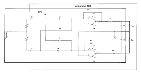
100351 For example, attention is directed to Fig. 6, which depicts non-
limiting
embodiments of apparatus 198 which comprise a circuit 600, connected to RF
power
supplies V3, V4, each representing an RF power supply for a pair of rods in a
quadrupole. In general, circuit 600 is similar to circuit 200, and comprises a
capacitors
C5, C6, similar to capacitors CI, C2 respectively, and a rectifying diode
circuit formed
from diodes D5, D6, D7, 08, similar to the rectifying diode circuit formed
from
capacitors DI , D2, D3, D9, respectively, of circuits 200. In addition,
circuit 600
comprises a first averaging circuit formed by resistor R8 and capacitor C7,
such that
average forward rectified RF voltage can be measured across resistor R30, and
a second
averaging circuit formed by resistor R9 and capacitor C8, such that average
reverse
rectified RF voltage can be measured across resistor R31.
[00361 Circuit 600 further comprises at least one operational amplifier ll5,
U6,
configured as a current to voltage converter, a negative input of at least one
operational
amplifier U5, U6 connected to the output of at least one diode 05, D6, D7, D8
in the at
least one rectifying diode circuit, a positive input of at least one
operational amplifier U5,
U6 at ground, and an output of at least one operational amplifier U5, U6 in a
feedback
loop with the negative input of at least one operational amplifier U5, U6, to
reduce
reverse leakage current from the at least one diode D5, D6, D7, D8.
j00371 For example, the negative input of operational amplifier U5 is
connected to the
output of diodes D5, D6, diode D5 connected to RF power supply V3 (via
capacitor C5),
9
CA 2788225 2017-06-12
CA 02788225 2012-07-26
WO 2011/041902
PCT/CA2010/001605
and diode D6 connected to RF power supply V4 (via capacitor C6). Taking diode
D5 as a
non-limiting example, as the negative input of operational amplifier U5 is
connected to
the output of diode D5, and the positive input of operational amplifier U5 is
grounded,
operational amplifier U5 acts as an inverting amplifier. And, as the negative
input of
operational amplifier U5 is in a feedback loop with the output of operational
amplifier
U5, the negative input generally matches the positive input, and as the
positive input is
grounded, V_=V+,-z0 (where V_ is the voltage at the negative input of
operational amplifier
U5, and V+ is the voltage at the positive input of operational amplifier 1J5).
Hence,
operational amplifier U5 reduces any current from diode D5.
[0038] Hence, when a reverse bias voltage is applied to diode D5, such that
the reverse
bias voltage drop across diode D5 is large, and consequently so is the leakage
current,
operational amplifier U5 reduces the reverse voltage drop via the feedback
loop. For
example, Fig. 3 further depicts a curve 350 representing a modelled voltage
drop across
diode D5, for example, when an RF voltage is applied to diode D5 from RF power
supply
V3. It is understood that curves 300 and 350 are depicted as being 180 out of
phase for
clarity. Curve 350 comprises a plurality of positive sections, represented in
part by
section 351a, and a plurality of negative sections, represented in part by
section 351b,
alternating there between as an RF voltage is applied. In general, section
351a represents
the reverse bias voltage drop across diode D1, for example, and section 351b
represents
the forward bias voltage drop across diode D1. It is understood from section
351a and
section 351b that the reverse bias voltage drop is similar to the forward bias
voltage drop
due to the reduction leakage current by operational amplifier U5. Furthermore,
from a
comparison of curves 300 and 350, it is understood that the reverse bias
voltage of diode
D5 of circuit 500 has been decreased in comparison to the reverse bias voltage
of diode
D1 of circuit 200 due to the reduction of reverse bias leakage current
provided by
operational amplifier U5.
[0039] It is further understood that operational amplifier U5 plays a similar
role in
reducing reverse bias leakage current in diode D6. It is yet further
understood that
operational amplifier U6 plays a similar role in reducing reverse bias leakage
current in
diodes D7, D8.
WO 2011/041902 PCT/CA20101001605
[00401 Hence the large reverse bias voltage drop across at least one of diodes
D5, D6,
D7, D8 in each respective rectifying diode circuit, is reduced by the at least
one
operational amplifier U5, U6, which leads to better stability in diodes D5,
D6, D7, D8,
and hence reduces mass drift in the quadrupole to which the RF voltage is
being supplied
and lengthens the life of diodes D5, D6, D7, D8 as breakdown of diodes D5. D6,
D7, 08
becomes less likely.
100411 It is further understood that apparatus 198 can comprise any suitable
number of
connectors for connecting to RF power supplies V3, V4 and/or the associated
quadrupole(s) to which RF voltage is being supplied. In some embodiments,
apparatus
198 comprises any suitable number of connectors such that the voltage across
resistor
R30 and/or R31 can be measured. In some embodiments, apparatus 198 further
comprises
an output to apparatus 199 and/or processor 185 such that the measured voltage
across
resistor R30 and/or R31 can be fed into a feedback loop with apparatus 199 for
controlling the RF voltage supplied to quadrupole 140 (and/or collision cell
150).
[0042] The values of capacitors C5, C6, C7, C8 and resistors R7, R8, R9, R12,
R30, R31
can be any suitable value and can be determined via any suitable circuit
modelling
software. Furthermore, the values of capacitors C5, C6, C7, C8 and
resistorsR7, R8, R9, R12
can depend on the desired gain of circuit 600 and or/the degree of averaging
desired. In
specific non-limiting embodiments, capacitors C5, C6 are each on the order of
a few pF,
capacitors C7, C8 are each on the order of a few nF, resistors R7, R12 are
each on the
order of a few hundred ohms, resistors R8, R9 are each on the order of a kilo-
ohm to tens
of kilo-ohms, and resistors R30, R31 are each on the order of a few megaohms.
Each of
diodes D5, D6, D7, D8 can comprise any suitable diode. In specific non-
limiting
exemplary embodiments, each of diodes D5, Db, 07, D8 can comprise a Schottky
diode
D1N5711, however any suitable diode is within the scope of present
embodiments. Each
of operational amplifiers U5, U6 can comprise any suitable operational
amplifier. In non-
limiting exemplary embodiments, each of operational amplifiers can comprise a
low
noise operational amplifier LT1806, however any suitable operational amplifier
is within
the scope of present embodiments. It is further understood that each of
operational
amplifiers is connected to suitable power supplies and/or power supplies
supplying
suitable voltages Vee, Vcc.
11
CA 2788225 2017-06-12
CA 02788225 2012-07-26
WO 2011/041902
PCT/CA2010/001605
[0043] Attention is now directed to Fig. 7 which depicts alternative
embodiments of
apparatus 198 comprising a circuit 700. Circuit 700 is similar to circuit 400,
and is
enabled to measure average rectified voltage from a single RF power supply V10
and
comprises a diode D11 analogous to diode D4, and a diode D12, analogous to
diode DIO,
diodes D11, D12 forming a rectifying diode circuit. Circuit 700 further
comprises
averaging circuits, a first averaging circuit comprising resistor R16 and
capacitor C12,
such that an average forward bias voltage can be measured across resistor R35,
and a
second averaging circuit comprising resistor R17 and capacitor C13, such that
an average
forward bias voltage can be measured across resistor R36. However, circuit 700
includes
an operational amplifier U7 for reducing the reverse bias current of diode
D11, and an
operational amplifier U8 for reducing the reverse bias current of diode D12,
as described
above. Similar values of capacitances and resistances, and similar diodes and
operational
amplifiers can be used as described above with reference to Fig. 6.
[0044] Attention is now directed to Fig. 8 which depicts alternative
embodiments of
apparatus 198 comprising a circuit 800. Circuit 800 is similar to circuit 500,
and is
enabled to measure average rectified voltage from a single RF power supply V11
and
comprises a diode D13 analogous to diode D4, and a diode D14, analogous to
diode D10,
diodes D13, D14 forming a rectifying diode circuit. Circuit 800 further
comprises an
averaging circuit comprising resistor R38 and capacitor C15, such that an
average
forward bias voltage can be measured across resistor R39. Reverse bias voltage
is passed
to ground via diode D14. However, circuit 800 includes an operational
amplifier U9 for
reducing the reverse bias current of diode D13, as described above. Similar
values of
capacitances and resistances, and similar diodes and operational amplifiers
can be used as
described above with reference to Fig. 6.
[0045] Attention is now directed to Fig. 9 which depicts alternative
embodiments of
apparatus 198 comprising a circuit 900. Circuit 800 is similar to circuit 900,
and is
enabled to measure average rectified voltage from a single RF power supply V12
and
comprises a diode D15 analogous to diode D13, and a diode D16, analogous to
diode
D14, diodes D15, D16 forming a rectifying diode circuit. Circuit 900 further
comprises a
first averaging circuit comprising resistor R41 and capacitor C17, such that
an average
forward bias voltage can be measured across resistor R42. Circuit 900 further
comprises s
12
WO 2011/041902
PCT/CA2010/001605
second averaging circuit comprising resistor R44 and capacitor C18, such that
an average
reverse bias voltage can be measured across resistor R45. Operational
amplifier U10 is
analogous to operational amplifier U9, for reducing reverse leakage current
from diode
D15. However, circuit 900 further comprises an operational amplifier Ul for
reducing the
reverse bias current of diode D16, in measurements of average reverse
rectified RF
voltage. Similar values of capacitances and resistances, and similar diodes
and
operational amplifiers can be used as described above with reference to Fig.
6.
(00461 It is further understood that apparatus 198 and/or circuit 600 and/or
circuit 700
and/or circuit 800 and/or circuit 900 can be provided in a method for
measuring RF
voltage supplied to a quadrupole from at least one RF power supply,
(0047I Those skilled in the art will appreciate that in some embodiments, the
functionality of mass spectrometer 100 can be implemented using pre-programmed
hardware or firmware elements (e.g., application specific integrated circuits
(AS1Cs),
electrically erasable programmable read-only memories (EEPROMs), etc.), or
other
related components. In other embodiments, the functionality of mass
spectrometer 100
can be achieved using a computing apparatus that has access to a code memory
(not
shown) which stores computer-readable program code for operation of the
computing
apparatus. The computer-readable program code could be stored on a computer
readable
storage medium which is fixed, tangible and readable directly by these
components, (e.g.,
removable diskette, CD-ROM, ROM, fixed disk, USB drive). Alternatively, the
computer-readable program code could be stored remotely but transmittable to
these
components via a modem or other interface device connected to a network
(including,
without limitation, the Internet) over a transmission medium. The transmission
medium
ran be either a non-wireless medium (e.g., optical and/or digital and/or
analog
conununications lines) or a wireless medium (e.g., microwave, infrared, free-
space
optical or other transmission schemes) or a combination thereof.
[00481 Persons skilled in the art will appreciate that there are yet more
alternative
implementations and modifications possible for implementing the embodiments,
and that
the above implementations and examples are only illustrations of one or more
embodiments. The scope, therefore, is only to be limited by the claims
appended hereto.
13
CA 2738225 2017-06-12