Note: Descriptions are shown in the official language in which they were submitted.
CA 02788751 2012-08-01
WO 2011/095212
PCT/EP2010/051313
1
Switching module for use in a device to limit and/or break the current of a
power
transmission or distribution line
The invention relates to a switching module which is arranged to be used in a
device
to limit and/or break an electrical current flowing through a power
transmission or
distribution line, where the switching module comprises at least one power
semiconductor switching element, a gate unit arranged to turn the at least one
power
semiconductor switch on and off, respectively, according to a switching
control
signal, and an energy storage capacitor arranged to provide power to a power
supply
input of the gate unit.
The invention stems originally from the field of high voltage direct current
(HVDC)
breakers and current limiters, i.e. of switching devices which are able to
limit and/or
break a direct current flowing through a power transmission line, where the
line is at
a voltage level above 50 kV. However, the invention is also applicable to
breakers for
medium voltage DC power distribution, i.e. for a DC voltage range between
about 1
kV and 50 kV, and bidirectional embodiments of the invention are even
applicable to
breakers for AC power transmission and distribution at any voltage level.
In EP 0867998 Bl, a solid-state DC breaker is described which comprises a
parallel
connection of at least one main power semiconductor switch and of a non-linear
resistor working as a surge arrester. When the DC breaker is operated to
interrupt a
DC current in a DC transmission or distribution line, the at least one main
power
semiconductor switch commutates the DC current into the non-linear resistor
which
then reduces the DC current by dissipating the stored energy in the DC line.
In
PCT/EP2009/065233, another solid-state DC breaker is presented which in
parallel
to the parallel connection of main power semiconductor switch and surge
arrester
contains a series connection of a mechanical high speed switch and of at least
one
auxiliary power semiconductor switch.
In practice, such solid state DC breakers, in order to be applicable for the
voltage
level of DC power transmission or distribution systems, need to contain a
considerable number of series connected main power semiconductor switches
since
a single power semiconductor switch has a comparatively low rated voltage. The
number of series connected main power semiconductor switches can easily reach
several hundreds in case of an HVDC voltage level of several hundred kV.
CA 02788751 2012-08-01
WO 2011/095212
PCT/EP2010/051313
2
With respect to the present invention, both the main power semiconductor
switches
as well as possibly present auxiliary power semiconductor switches of a DC
breaker
or DC current limiter each represent a switching module, i.e. they comprise,
besides
one or several power semiconductor switching elements, a gate unit and an
energy
storage capacitor. Such switching modules are for example described in detail
in EP
0 868 014 Bl, where the energy storage capacitor is connected via a DC/DC
converter to the power supply input of the gate unit. The energy stored in the
capacitor is transformed via the DC/DC converter into the DC supply voltage
required
by the gate unit for its usual operation of turning the at least one power
semiconductor switching element on and off. The energy storage capacitor
itself is
connected to the so called high voltage primary circuit, i.e. it is connected
to the
same circuit and thereby to the same high voltage level as the at least one
power
semiconductor switching element of that particular switching module. Whenever
the
at least one power semiconductor switching element is in the blocking ¨ i.e.
non-
conducting ¨ switching state, the energy storage capacitor is charged.
With respect to DC breakers and DC current limiters containing main and/or
auxiliary
power semiconductor switches, this known way to supply the gate units of the
switching elements appears to be problematic, as under normal operating
conditions
the DC breaker or DC current limiter is supposed to be conducting for a long
period
of time, preferably a year or even more, without any need for a switching
operation.
Accordingly, at least a part of their power semiconductor switching elements
is
permanently conducting, thereby not offering a blocking state which would
allow for
the required charging or recharging of the corresponding energy storage
capacitors.
This makes it difficult to ensure that enough power can be supplied to the
gate unit in
case the power semiconductor switching elements are to be operated. In
addition,
the putting of a DC breaker into operation usually means, that the
corresponding
power transmission or distribution line is afterwards disconnected from the DC
grid,
thereby leaving the primary circuit at zero voltage. Accordingly, a charging
or
recharging of the energy storage capacitors of the switching modules of a DC
breaker is only possible during the rare and short periods of time when the
breaker is
opened. If no repeated and regular charging of the energy storage capacitors
can be
ensured, the reliability of the corresponding DC breaker or DC current limiter
is
reduced considerably.
A different solution for providing power to the gate units of power
semiconductor
switches is known from medium voltage converter applications, where a remote
CA 02788751 2014-11-04
3
power supply via pulse transformers is used, i.e. the power supply works
independently of the primary circuit. However, this solution is inapplicable
to high
voltage levels due to design and cost reasons since the insulation of every
pulse
transformer needs to withstand at least the nominal DC voltage, which for high
voltage applications means several hundred kV. In case of high voltage DC
breakers,
the overvoltage stress during an opening action requires even an insulation
level of
almost twice the DC voltage.
It is an object of the present invention to present a solution for a switching
module for
use in a DC breaker or DC current limiter, in particular for HVDC
applications, with
which the reliability of the switching module and thereby of the DC breaker or
the DC
current limiter is increased.
This object is achieved by a switching module which further comprises power
transformation means arranged to receive power via an optical power signal, to
transform the optical power signal into an electrical power signal and to
provide the
electrical power signal to the energy storage capacitor.
According to an aspect of the invention, there is provided a device to limit
and/or
break an electrical current flowing through a power transmission or
distribution line,
the device comprising at least one switching module comprising:
at least one power semiconductor switching element;
a gate unit arranged to turn the at least one power semiconductor switching
element on and off, respectively, according to a switching control signal;
an energy storage capacitor arranged to provide power to a power supply
input of the gate unit; and
power transformation means arranged to receive an optical power signal, to
transform the optical power signal into an electrical power signal and to
provide the
electrical power signal to the energy storage capacitor,
wherein the switching module is arranged to separate from the optical power
signal an electrical control signal and to provide the electrical control
signal to the
gate unit, and
wherein the electrical control signal comprises said switching control signal.
According to another aspect of the invention, there is provided a device to
limit and/or
break an electrical current flowing through a power transmission or
distribution line,
the device comprising at least one switching module comprising:
CA 02788751 2014-11-04
3a
at least one power semiconductor switching element and at least one diode
or diode function, where a diode or diode function is in antiparallel with a
power
semiconductor switching element;
a gate unit arranged to turn the at least one power semiconductor switching
element on and off, respectively, according to a switching control signal;
an energy storage capacitor arranged to provide power to a power supply
input of the gate unit;
power transformation means arranged to receive an optical power signal, to
transform the optical power signal into an electrical power signal and to
provide the
electrical power signal to the energy storage capacitor; and
a diode monitoring means adapted to monitor the blocking functionality of
said at least one diode or diode function whenever the corresponding power
semiconductor switching element are turned-off and no main current is flowing
through the at least one diode or diode function to be monitored, where during
the
monitoring a positive test voltage is applied to the forward direction of the
at least one
switching element and a failure information is generated in case the test
voltage is
not maintained.
According to the invention, the power supply of the gate unit is made
independent of
the voltage conditions in the primary circuit by providing an optical power
supply to
the energy storage capacitor. Thereby, the charging and recharging of the
energy
storage capacitor can occur regularly at predetermined intervals of time, so
that it can
always be ensured that enough power is available for the gate unit to operate
the
corresponding power semiconductor switching element or elements whenever it is
required. The operability and reliability of the DC breaker or DC current
limiter
containing such a switching module is thereby increased considerably. Since an
optical power signal, i.e. light, preferably laser light, transmitted via a
fiber optic
cable, is used instead for an electrical power signal, the insulation problem
of the
above described pulse transformer solution is overcome.
In a preferred embodiment of the invention, the optical power signal is a low
power
signal of less than 1 Watt. Since low power equipment usually features a
larger
reliability compared to equipment for higher power levels, the use of a low
power
optical power supply helps to increase the reliability of the switching module
further.
If a low power optical power supply is used, certain measures need to be taken
to
keep the internal power demand of the gate unit at a low level. A preferred
way to
CA 02788751 2012-08-01
WO 2011/095212
PCT/EP2010/051313
4
achieve this is to reduce the number of functions performed by the gate unit
to a
minimum level.
As was mentioned in the introduction, today's DC breakers or DC current
limiters
which are applicable to the medium and high voltage levels of DC power
distribution
and transmission systems, need to contain a considerable number of series
connected switching modules. In series-connections, the question of an equal
voltage distribution during dynamic and transient processes is important in
order to
avoid undesired voltage stress on some of the switching modules due to
differing
switching characteristics of the power semiconductor switching elements of
different
switching modules.
One of the functions that known gate units perform in high voltage converter
valves,
where in the valves several power semiconductor switches are connected in
series
and each power semiconductor switch is equipped with its own gate unit, is to
ensure
an equal voltage distribution between the series connected switches during
dynamic
and transient processes
This function is according to a preferred embodiment of the invention not
performed
by the gate unit but instead by an ROD snubber circuit, which is contained in
the
switching module and is connected in parallel to the at least one power
semiconductor switching element. The ROD snubber circuit comprises at least
one
resistor, at least one capacitor and at least one diode. ROD snubbers are
known in
the art and are for example disclosed in WO 96/27230. The ROD snubber can be
arranged for both unidirectional and bidirectional switching modules (see
below),
where the unidirectional ROD snubber comprises a series connection of a diode
and
a capacitor for one current direction, with a resistor in parallel with the
diode, and the
bidirectional ROD snubber comprises in addition a series connection of a diode
and a
capacitor for the other current direction, with again a resistor in parallel
with the
diode.
During turn-off of the power semiconductor switching element, the current
through
the switching element commutates via the one of the snubber diodes, which
corresponds to the current direction, into the at least one snubber capacitor.
As is
described in the introduction above, a DC breaker typically contains a group
of
several series connected switching modules which are together connected in
parallel
with a non-linear resistor working as a surge arrester. A DC current limiter
contains
CA 02788751 2012-08-01
WO 2011/095212
PCT/EP2010/051313
several of such groups. When a DC breaker or a DC current limiter is operated,
the
switching modules of these groups are turned-off simultaneously. Accordingly,
the
same commutation of the current into the snubber circuit takes place for all
of the
series connected switching modules per group. As a result, the snubber
capacitors of
5 each group are charged until the sum of the snubber capacitor voltages
per group is
high enough for the arrester of that group to take over the current. When the
groups
of switching modules are switched on again, the snubber capacitors are
discharged
via the corresponding snubber resistors. This leads to certain losses which,
however,
are of no relevance in DC breaker and DC current limiter applications due to
the rare
occasion of an operating action.
Apart from the equal dynamic voltage distribution, the ROD snubber has some
further
advantages. Due to the presence of at least one capacitor in the ROD snubber,
the
rate of rise of the voltage across the corresponding at least one power
semiconductor
switching element is limited. As a result, individual switching
characteristics, like for
example individual turn-off delays of the power semiconductor switching
elements,
which may differ between series connected switching modules, are no longer of
concern.
In addition, the limited rate of rise of the voltage shows its advantage in
connection
with the below described parallel connection of IGBT or BIGT modules, since
again
different switching delays are no longer of major concern, thereby eliminating
the risk
of damaging high frequency oscillations between the modules. In general, it
can be
stated that due to the ROD snubber it becomes possible to connect IGBT or BIGT
modules in series and/or in parallel with each other, without at the same time
needing
to provide for a complex and power demanding gate unit to take care of an even
voltage distribution and of possible high frequency oscillations.
A further advantage of the ROD snubber is that, when the power semiconductor
element is turned off, the snubber capacitor causes the voltage to start at
zero, i.e.
the switching is performed at zero voltage. As a result, less instantaneous
losses are
generated during the turning-off and therefore during the operating of the DC
breaker
or DC current limiter. The reduced losses allow for higher turn-off currents
and/or a
larger number of repetitive switching events before a thermal limit of the
power
semiconductor switching element is reached.
CA 02788751 2012-08-01
WO 2011/095212
PCT/EP2010/051313
6
In a further embodiment of the invention, the gate unit is connected to the
gate of the
power semiconductor switching element via an H-bridge which produces and
outputs
the bipolar DC voltage required to drive the gate of the at least one power
semiconductor switching element, where the H-bridge is supplied by a unipolar
DC
voltage and outputs a symmetrical bipolar DC voltage, for example 15V.
According
to this embodiment, the gate unit can operate internally with a unipolar DC
voltage,
opposed to the gate unit known from EP 0 868 014 B1 which operates internally
with
bipolar DC voltages and thereby two internal power supplies. Using the
unipolar
operating DC voltage reduces the internal power demand of the gate unit even
further and makes it even more suitable to be used with a low power supply
level.
When using two internal power supplies instead of an H-bridge, unsymmetrical
DC
voltages can be produced by the gate unit, for example +18V and -5V.
In another embodiment of the invention, the switching module further comprises
a
control signal detector which is arranged to separate from the received
electrical
power signal an electrical control signal and to provide the electrical
control signal to
the gate unit. In other words, a control signal which in particular comprises
the
switching control signal to initiate the gate unit to turn the at least one
power
semiconductor switching elements on or off is incorporated into the same
optical
signal which also contains the power signal and it is still contained in the
electrical
power signal after the signal transformation by the power transformation
means. In
this way, the need of an additional fiber optic cable is eliminated.
According to a further embodiment of the invention, the gate unit of the
switching
module is arranged to generate status information on the functionality of at
least one
of the elements of the switching module, and the switching module comprises
further
signal transformation means arranged to transform the status information into
an
optical information signal and to send out the optical information signal to a
central
control unit. That the status information is sent out optically is due to the
fact that the
switching modules are in a DC breaker or DC current limiter application
arranged at a
high voltage level of up to several hundred kV. Using optical communication
simplifies the design and increases the reliability of the communication
system.
By providing status information to a central control unit, it becomes possible
that the
central control unit takes care of each connected switching module
individually, for
example by sending back a control signal to start a specific test routine in
case that a
suspicious status is reported which requires further investigation. The
central control
CA 02788751 2012-08-01
WO 2011/095212
PCT/EP2010/051313
7
unit may at the same time generate the above mentioned control signal which
initiates the turning on and off of the at least one power semiconductor
switching
device. In DC breaker and DC current limiter applications, the switching of
the
switching modules can be delayed up to tens of microseconds until a sufficient
number of switching modules is ready for switching, since the actual operation
of the
DC breaker or DC current limiter needs to occur less instantaneously than it
is for
example required in a converter application. As a result, it can be ensured
that the
switching modules are turned on or off as simultaneously as possible. In other
words,
by exchanging status information with the central control unit, it becomes
possible to
implement a handshake protocol between the central control unit and all the
switching modules of the DC breaker or DC current limiter, where the handshake
protocol arms and synchronizes the gate units and sends out the actual turning-
on or
turning-off control signal only when all or ¨ in case of redundancy ¨ enough
switching
modules are ready.
The at least one power semiconductor switching element of the switching module
can be of different type and design, depending on the operational and cost
requirements of the DC breaker or DC current limiter where the switching
module is
to be used in. In the following, some preferred types are briefly described,
which are
suitable to be used either in a unidirectional or in a bidirectional DC
breaker or DC
current limiter. In order to be applicable to a bidirectional DC breaker or a
DC current
limiter, the unidirectional power semiconductor switching elements need to be
duplicated and the duplicate needs to be arranged for the opposite current
direction,
i.e. in anti-parallel or anti-serial direction to the original power
semiconductor
switching element.
In one unidirectional type of the at least one power semiconductor switching
element,
the switching element comprises a first module containing one first IGBT or a
first
parallel connection of several IGBT as well as one first diode or a first
parallel
connection of several diodes, where the diode or diodes are connected in anti-
parallel with the IGBT or parallel connection of IGBT. If one or several
parallel-
connected IGBT and diodes are used, depends on the current level which is to
be
achieved with the power semiconductor switching element, i.e. the higher the
number
of parallel-connected IGBT and diodes the higher the rated current, where all
parallel-connected IGBT are controlled via the same gate unit.
CA 02788751 2012-08-01
WO 2011/095212
PCT/EP2010/051313
8
A bidirectional power semiconductor switching element can be achieved by
connecting a suitable number of above modules in anti-parallel or anti-serial
connection, where an anti-parallel connection is possible in case that the
IGBT have
reverse blocking capability. In other words, the switching module then further
comprises at least a second module connected in anti-parallel or anti-serial
with the
first module, the second module containing one second IGBT or a second
parallel
connection of several IGBT and one second diode or a second parallel
connection of
several diodes, where the diode or diodes are again connected in anti-parallel
with
the IGBT or parallel connection of IGBT.
The first and second modules may in practice be based on different physical
packaging concepts of the chips of the IGBT and diodes. Either, each module
corresponds to one single package containing an integration of IGBT and
corresponding anti-parallel diodes, or, all parallel connected IGBT of the
same
current direction are integrated in one package and all parallel connected
diodes of
the same current direction are integrated in another package. The latter
design would
overcome a problem which may occur in connection with the first design. In the
first
design, the diodes of different packages may stem from different production
cycles,
and therefore they may slightly differ in their characteristics, such as the
forward
voltage drop. Since the diodes have a negative temperature coefficient,
different
forward voltage drops may lead to an undesired current flow between the diodes
which could result in a so called thermal runaway of the diode chips, i.e. in
an
increase in temperature due to the current flow which increases the current
flow even
further. When all parallel diodes of the same current direction of the power
semiconductor switching element are integrated in the same package, as
proposed
in the second design, it is ensured that their characteristics match as
closely as
possible with each other, thereby minimizing the risk of thermal runaway.
In a special embodiment of the above described type of power semiconductor
switching element, the diodes are line commutated diodes. Usually, so called
fast
recovery diodes are used as anti-parallel diodes for IGBT, since they are
especially
suitable for the fast switching applications that IGBT are usually intended
for.
However, in the case of DC breakers and DC current limiters, no fast switching
actions are required, so that line commutated diodes, such as known from
standard
50 Hz rectifier applications, may be used instead. Since line commutated
diodes
have a lower voltage drop compared to fast recovery diodes, the losses of
above
CA 02788751 2012-08-01
WO 2011/095212
PCT/EP2010/051313
9
described first and second modules may be reduced. In addition, line
commutated
diodes are less costly.
In an alternative unidirectional type of power semiconductor switching
element, the
switching element comprises a first module containing one first reverse
conducting
IGBT or a first parallel connection of several reverse conducting IGBT. In a
reverse
conducting IGBT, the IGBT and the anti-parallel diode function are directly
integrated
in one common chip. Reverse conducting IGBT are for example described in the
European patent application 09159009.1 and are also called Bi-mode Insulated
Gate
Transistor (BIGT). As mentioned above, a parallel connection of several such
BIGT
provides for a higher rated current of the power semiconductor switching
element.
A bidirectional power semiconductor switching element can be achieved by
connecting two or more BIGT-modules in anti-serial connection. Accordingly, it
is
suggested that the above power semiconductor switching element further
comprises
a second module connected in anti-serial connection with the first module, the
second module containing one second reverse conducting IGBT or a second
parallel
connection of several reverse conducting IGBT.
The use of BIGT instead of separate IGBT and anti-parallel diodes implies
several
advantages.
One advantage is that the forward voltage drop of the integrated diode shows a
positive temperature coefficient, so that the problem of a possible thermal
runaway is
avoided.
In case of a special embodiment of a bidirectional DC breaker based on BIGT,
the
power semiconductor switching elements would each comprise an anti-serial
connection of two BIGT, where the two BIGT are vertically integrated in one
and the
same package. In a typical bidirectional DC breaker application, the current
flows in
one and the same direction for a considerably long period of time, which in
case of
common IGBT with separate diode means that the silicon area of the power
semiconductor switching elements of the bidirectional DC breaker is only
partially
used. Opposed to that, due to the vertical integration, the silicon area of
the
bidirectional BIGT packages can be fully utilized resulting in either a minor
number of
chips for the same current rating or in an increase of the current capability
for a given
number of chips per package.
CA 02788751 2012-08-01
WO 2011/095212
PCT/EP2010/051313
A third advantage is that the functionality of the diode can easier be
monitored in
case of a BIGT than in case of separate IGBT and diode.
5 In general, it is advantageous to provide the switching module with an
additional
diode monitoring means which is arranged to perform a test of the blocking
functionality of the anti-parallel diode or diodes and which thereby can
indicate if the
corresponding IGBT in the power semiconductor switching element is available
for
normal operation or not. This is recommended since it may happen on rare
10 occasions that the anti-parallel diode, or diodes, breaks down when the
corresponding IGBT is in the turn-off or non-conducting state, which may have
serious consequences. In fast switching applications, it is possible to test
the
blocking functionality of the diodes frequently when the corresponding IGBT is
in the
non-conducting state and no main current is flowing through the diode.
However, in a
DC breaker or DC current limiter, where at least part of the IGBT are turned
on
continuously, this is not in the same way possible for the corresponding
diodes.
Nevertheless, it is important to get information on defective diodes prior to
the
opening of a DC breaker or to the putting into operation of a DC current
limiter, since
such defective diodes could result in a fatal damage.
Therefore, for switching modules containing separate IGBT and diodes it is
suggested to provide a diode monitoring means which is adapted to monitor the
blocking functionality of the diode or diodes whenever the corresponding IGBT
are
turned-off and no main current is flowing through the diode or diodes to be
monitored. In other words, a test is performed as often as possible, where for
some
DC breaker configurations this may mean that a test can only be performed
during
maintenance, while for other configurations, such as the DC breaker described
in
PCT/EP2009/065233, the test can be performed continuously for those switching
modules which are not carrying the primary current. The test includes simply
to apply
a minor positive test voltage in forward direction of the turned-off IGBT and
to check
whether this voltage is maintained or whether it decreases and possibly even
breaks
down due to failure of the diode. If the latter occurs, a failure information
can be
generated, for example by the gate unit, and sent as an optical information
signal to a
central control unit. In connection with the above described ROD snubber, a
further
way of testing the functionality of the anti-parallel diodes becomes possible:
in a DC
breaker or DC current limiter which contains several switching modules in
series
connection, this further test is performed when the DC breaker or DC current
limiter
CA 02788751 2012-08-01
WO 2011/095212
PCT/EP2010/051313
11
is turned on and the current flows in forward direction through the series-
connected
IGBT. For testing the functionality of the diodes, one or several of the
series-
connected IGBT can now be actively turned off for a very short period of time,
preferably a couple of microseconds, until the current flowing through the
turned-off
IGBT has started to commutate to the corresponding ROD snubber circuit and
until
the voltage across the ROD snubber has started to rise slightly. As soon as
the
voltage rise is detected, the one or several IGBT are switched on again, where
the
voltage rise can be detected in a simple way by checking whether a predefined
voltage limit is exceeded, where the voltage limit lies at a comparatively low
voltage
level of preferably a couple of hundred V up to a few kV only. If no voltage
rise can
be detected, a failure information is generated. In this way, testing of the
diodes in
the switching modules becomes possible without interfering with the operation
of the
DC breaker or DC current limiter.
As becomes clear from the above, it is generally difficult to generate
reliable
information on the blocking capability of the diodes for the switching module
configuration with separate IGBT and diodes. Opposed to that, it is possible
to detect
failure of the integrated diode function in a BIGT during both the turn-on and
the turn-
off state of the corresponding IGBT. The possible detection of a failing or
failed diode
function in a BIGT during practically all of the operating states of the BIGT
in DC
breaker applications, is due to the fact that a defective integrated diode
function can
be observed by a clear deterioration or even breakdown of the gate-emitter
voltage of
the corresponding IGBT. Therefore an increased gate emitter leakage current
can be
used as an indication or monitor for an irreversible damage of either the
diode
function or the IGBT of the BIGT. Accordingly, the suggested diode monitoring
means for a switching module containing BIGT is adapted to monitor the
blocking
functionality of the diode function or diode functions of the reverse-
conducting IGBT
by generating a failure information in case the gate-emitter voltage across
the turned-
on or turned-off reverse-conducting IGBT breaks down. Due to the possibility
to
perform the test both in the turn-on and turn-off state of the BIGT, there
exist many
more chances to derive an information on the blocking capability of the diode
function
in the BIGT compared to the solution with separate IGBT and diode, thereby
increasing the reliability of the DC breaker or DC current limiter
considerably.
Apart from the dynamic voltage distribution discussed above in connection with
the
ROD snubber, it is also advantageous if the steady-state voltage distribution
of series
connected switching modules is kept as equal as possible in order to avoid
increased
CA 02788751 2012-08-01
WO 2011/095212
PCT/EP2010/051313
12
voltage stress on some of the modules. According to a further embodiment of
the
invention, it is therefore suggested that a non-linear, voltage-limiting
resistor is
connected in parallel with the at least one power semiconductor switching
element.
Such a non-linear, voltage-limiting resistor not only ensures equal steady-
state
voltage distribution, but in addition limits overvoltages when the arrester of
a group of
series connected switching modules takes over the current from the snubber
circuits
of that group. The arrester of a group of series connected switching modules
is in the
following also called main arrester. Further advantages of the non-linear,
voltage
limiting resistor in a switching module are that it allows for a reduction in
size of the
snubber capacitor of that module, that it enables for larger capacitor
tolerances
between different modules and that it simplifies the mechanical design of the
current
commutation path for the main arrester.
The invention and its embodiment will now be explained with reference to the
appended drawings in which:
Fig. 1 shows a first base element containing power semiconductor
switching
elements arranged for unidirectional applications,
Fig. 2 shows a second base element containing power semiconductor
switching elements arranged for bidirectional applications,
Fig. 3 shows a third base element containing power semiconductor switching
elements arranged for bidirectional applications,
Fig. 4 shows a fourth base element containing power semiconductor
switching
elements arranged for bidirectional applications,
Fig. 5 shows a first example for a DC breaker,
Fig. 6 shows a second example for a DC breaker,
Fig. 7 shows an example for a DC current limiter,
Fig. 8 shows a first embodiment of a switching module,
Fig. 9 shows a second embodiment of a switching module,
Fig. 10 shows a third embodiment of a switching module,
Fig. 11 shows a fourth embodiment of a switching module,
Fig. 12 shows an arrangement of a central control unit and the
switching
modules of a DC breaker,
Fig. 13 shows an arrangement of power semiconductor switching elements
of a
switching module.
Fig. 1 shows a first base element 6a containing power semiconductor switching
elements arranged for unidirectional applications. The power semiconductor
CA 02788751 2012-08-01
WO 2011/095212
PCT/EP2010/051313
13
switching elements are an IGBT 1 of a first current direction 4 and a free-
wheeling
diode 2 connected in anti-parallel to the IGBT 1.
In Fig. 2, a second base element 6b can be seen which comprises a parallel
connection of the IGBT 1 of the first current direction 4 and of an IGBT 3 of
a second,
opposite current direction 5. Accordingly, the second base element 6b is
suitable for
bidirectional applications.
In Fig. 3, a third base element 6c is shown which comprises a series
connection of
the IGBT 1 of the first current direction and the IGBT 3 of the opposite,
second
current direction, which is in other words an anti-serial connection of two
IGBT. Each
IGBT has a free-wheeling diode 2 and 7, respectively, connected in anti-
parallel. The
base element 6c is suitable for bidirectional applications.
A fourth base element 6d is shown in Fig. 4. It comprises as power
semiconductor
switching elements a reverse-conducting IGBT of the first current direction,
which is
also called a BIGT 8 (Bi-mode Insulated Gate Transistor), and in series with
the BIGT
8 a reverse-conducting IGBT of the second current direction, called BIGT 9.
The
BIGT 8 and 9 are accordingly connected in an anti-serial manner, meaning that
also
the fourth base element 6d is suitable for bidirectional applications.
The base elements 6a-6d may be used in a DC breaker 14 according to the
example
depicted in Fig. 5. The DC breaker 14 is suitable for medium or high voltage
applications, and it is connected in series with a DC power distribution or
transmission line 13. In case that the primary current in line 13 needs to be
interrupted in one direction only, base elements 6a may be used, while in case
that
the primary current in line 13 needs to be interrupted in both possible
directions, base
elements 6b or 6c or 6d are to be used. The DC breaker 14 comprises a main
breaker 10 containing a series-connection of several tens up to several
hundreds of
base elements 6, ¨ depending on the voltage level ¨, as well as a non-linear
resistor,
which is also called main arrester 11 and which is connected in parallel with
the main
breaker 10. In series with the DC breaker 14, a reactor 12 is arranged for
limiting the
current rate in the line 13. Under normal operating conditions of line 13, all
IGBT or
BIGT in the base elements 6 are turned-on, i.e. DC breaker 14 is conducting
the
primary current of line 13. In case that the primary current is to be
interrupted, for
example if a fault has occurred in line 13, all IGBT or BIGT are to be turned-
off
CA 02788751 2012-08-01
WO 2011/095212
PCT/EP2010/051313
14
simultaneously, in order for the primary current to commutate to the main
arrester 11
which will then reduce the current to zero.
Another example for a DC breaker 17, for which base elements 6a-6d may be
used,
is shown in Fig. 6. In addition to the main breaker 10 and the main arrester
11, there
is provided a series-connection of a high speed switch 15 and an auxiliary
breaker 16
connected in parallel to the main breaker 10 and the main arrester 11. The
auxiliary
breaker 16 contains just one base element 6. The high speed switch 15 is a
mechanical switch. In series with the DC breaker 17, again a reactor 12 is
placed for
current rate limitation.
It is interesting to note that in case that the base elements 6 used in the DC
breaker
configurations of Figs. 5 and 6 are bidirectional base elements of either type
6b, 6c or
6d, the same configurations are also suitable to be used as AC breakers for AC
power distribution or transmission lines.
In Fig. 7, an example for a DC current limiter 18 is shown, where the DC
current
limiter 18 comprises a series connection of multiple DC breakers 14. In other
words,
the DC current limiter 18 contains multiple groups of series connected base
elements
6, where each group comprises in parallel with the base elements 6 a main
arrester
11. The DC current limiter 18 is connected in series with a current rate
limiting
reactor 12 and with a DC power distribution or transmission line 13. In case
that the
primary current in line 13 is to be limited or reduced, a suitable number of
DC
breakers 14 is opened, so that the corresponding non-linear resistors may
dissipate
the undesired amount of electrical energy. In its most reduced form, a DC
current
limiter should contain two breakers 14, in the following called a first and a
second
breaker. The protective level of the main arrester of the first breaker
corresponds to
the nominal DC voltage level of line 13. When the current through line 13 is
to be
limited or reduced, the first breaker would be opened. The protective level of
the
main arrester of the second breaker can be set to a value below the nominal DC
voltage level of line 13, for example 50% of it. After the first breaker is
opened, the
second breaker can be used to interrupt the current in line 13 by opening the
second
breaker as well.
The invention is now further explained with respect to Figs. 8 to 12. In order
for the
base elements 6 in a DC breaker or a DC current limiter to be operated, so
called
gate units are required which cause the corresponding IGBT or BIGT to be
turned on
CA 02788751 2012-08-01
WO 2011/095212
PCT/EP2010/051313
or off, according to a control signal generated by a central control unit in
dependence
on the status of line 13. Accordingly, the base elements 6 of DC breakers 14
or 17 or
of DC current limiter 18 actually contain more than just the power
semiconductor
switching elements. In fact, each base element 6 can be replaced by a
switching
5 module 38, where the switching module 38 comprises amongst others a gate
unit 31.
Different embodiments of the switching module 38 will now be described, where
for
each embodiment the power semiconductor switching elements actually shown can
be replaced by the power semiconductor switching elements belonging to another
suitable one of the base elements 6a-6d and also by further combinations of
them as
10 explained below.
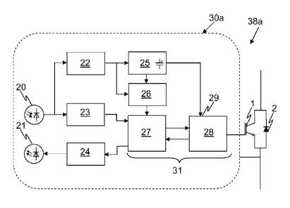
A first embodiment 38a of the switching module is depicted in Fig. 8, and it
comprises
besides an IGBT 1 and an anti-parallel diode 2 a first embodiment 30a of a
gate
driving module connected to the gate of the IGBT 1. The gate driving module
30a
15 comprises power transformation means in form of a photodiode 20, a DC/DC
converter 22, an energy storage capacitor 25 and a gate unit 31. The
photodiode 20
is arranged to receive an optical power signal, to transform the optical power
signal
into an electrical power signal and to provide the electrical power signal via
the
DC/DC converter 22 to the energy storage capacitor 25, thereby charging or
recharging the energy storage capacitor 25 from a power source which is
independent of the status or switching condition of the circuit, also called
primary
circuit, where the IGBT 1 and diode 2 are a part of. The optical power signal
is
hereby a low power signal of less than 1 Watt.
The energy storage capacitor 25 is connected to a power supply input 29 of the
gate
unit 31 in order to supply a gate driver and supervision module 28 with the
required
energy to drive the gate of IGBT 1. The gate unit contains apart from the gate
driver
and supervision module 28 a gate unit control module 27. The gate unit control
module 27 receives an electrical control signal from a control signal detector
23,
where the control signal detector 23 is arranged to separate the electrical
control
signal from the electrical power signal which is output by the photodiode 20.
Accordingly, the optical power signal received by the photodiode 20 also
contains an
optical information signal which after the transformation into an electrical
signal is still
present. The photodiode 20 is connected via a first fiber optic cable 51 to a
central
control unit 50 (see Fig. 12).
CA 02788751 2012-08-01
WO 2011/095212
PCT/EP2010/051313
16
The gate unit control module 27 processes the electrical control signal and
outputs a
resulting turn-on or turn-off order signal to the gate driver and supervision
module 28,
which accordingly causes the IGBT 1 to turn on or turn off. The gate unit
control
module 27 further receives different information, such as information
delivered by the
gate driver and supervision module 28 on the status of the IGBT 1 and
information
delivered by a power supervision unit 26 on the status of the elements
involved in the
power supply of the gate driver and supervision module 28, i.e. information on
the
status of the energy storage capacitor 25 and of the DC/DC converter 22. The
different information are processed by the gate unit control module 27 and
then
provided as status information via a signal transmitting module 24 to a signal
transformation means, which in this example is a light emitting diode 21. The
light
emitting diode 21 is connected via a second fiber optic cable 52 to the
central control
unit 50 (see Fig. 12), which in reaction to the received status information
may adapt
the control signal sent via the optical power signal to the photodiode 20.
A second embodiment 38b of the switching module is shown in Fig. 9, where the
second embodiment 38b contains the same gate driving module 30a as the first
embodiment 38a. One detail of the gate driver and supervision module 28 is
shown
here which is not shown in Fig. 8. From Fig. 9, it can be seen that the gate
driver and
supervision module 28 and thereby the gate unit 31 is connected via an H-
bridge to
the gate of the at least one power semiconductor switching element, which here
is an
IGBT 1 with an anti-parallel diode 2, where the H-bridge is supplied by a
unipolar DC
voltage of 15 V and outputs a bipolar DC voltage of 15 V. Accordingly, the
internal
power demand of the gate unit 31 is reduced to some extent.
In addition to the first embodiment 38a, the second embodiment 38b of the
switching
module contains a non-linear, voltage-limiting resistor 32 in parallel with
the at least
one power semiconductor switching elements as well as an RCD snubber circuit
consisting of a series connection of a diode 33 and a capacitor 34 as well as
a
resistor 35 in parallel with the diode 33, where the RCD snubber circuit
itself is also
connected in parallel with the at least one power semiconductor switching
element.
The orientation of the diode 33 is the same as the orientation of the IGBT 1.
The
RCD snubber circuit is mainly responsible for an equal dynamic voltage
distribution in
a series connection of several switching modules 38, as would for example be
applicable to the DC breakers 14 and 17 or the DC current limiter 18, when the
base
elements 6 are replaced with switching modules 38. The non-linear, voltage-
limiting
CA 02788751 2012-08-01
WO 2011/095212
PCT/EP2010/051313
17
resistor 32 mainly ensures an equal steady-state voltage distribution in such
a series
connection of switching modules 38.
In the third embodiment 38c of the switching module according to Fig. 10, in
addition
to the one IGBT 1 and the one diode 2 of the first and second embodiments, 38a
and
38b, respectively, which together form a first module referenced by the letter
a, a
second module, referenced by the letter b, containing a second IGBT 1 and a
second
anti-parallel diode 2 is connected in anti-serial connection with the first
module.
Accordingly, the switching module 38c can be applied to a bidirectional DC
breaker
or a bidirectional DC current limiter.
As already described, further and alternative combinations of IGBT and diodes
are
possible. An example is shown in Fig. 13, where both the first and the second
module each comprise not only one but two parallel connected IGBT la or lb and
corresponding anti-parallel diodes 2a or 2b, respectively. The physical
packaging of
the two modules can either be in the form of one package for each pair of IGBT
and
corresponding diode, or in the form of a first package with all the IGBT la of
the first
current direction, a second package with all the IGBT lb of the other second
current
direction, and a third and fourth package with all the diodes 2a and 2b,
respectively,
also according to their current direction. This latter type of packaging,
which provides
a considerable reduction of the risk of thermal runaway, as was described
above, is
depicted in Fig. 13 by the dotted lines.
The third embodiment 38c of the switching module comprises apart from the
first and
second modules of IGBT and diodes a second embodiment 30b of the gate driving
module, where this second embodiment 30b comprises two further units not
contained in the first embodiment 30a. One of the further units is a diode
monitoring
means 37, the task of which is to monitor the blocking functionality of the
diodes 2 in
the first module. The monitoring is done by applying a positive test voltage
in forward
direction to the IGBT la or lb, respectively, whenever they are turned-off and
when
no main current is flowing through the corresponding diodes. By checking
whether
this test voltage is maintained or not, a failing or failed diode 2a or 2b,
respectively,
can be recognized. Taking the example of the DC breaker 17, the diode
monitoring
can be performed for the diodes in the main breaker 10 during normal
operation,
since the main or primary current flows during that time through the auxiliary
breaker
16 and the high speed switch 15.
CA 02788751 2012-08-01
WO 2011/095212
PCT/EP2010/051313
18
The other further unit of the second embodiment 30b of the gate driving unit
is an
auxiliary recharge circuit 36 which in addition to the optical power supply
provides
energy to the energy storage capacitor 25 whenever possible and which takes
its
energy from the primary circuit where the IGBT 1 and the diodes 2 are
connected to.
However, as is described above, the occasions for recharging from the primary
circuit, i.e. the occasions when the IGBT 1 are turned off in a DC breaker or
DC
current limiter application are usually quite rare. Both the monitoring and
the auxiliary
recharging are initiated by a corresponding start signal sent from the gate
driver and
supervision module 28 to the diode monitoring means 37 and to the auxiliary
recharge circuit 36, respectively. These start signals can either be generated
internally in the switching module, by the gate unit control module 27 or by
the
auxiliary recharge circuit 36 itself in case it is intelligent enough to adapt
to the
conditions in the primary circuit, or they can be sent in the form of a
corresponding
control signal via the first fiber optic cable 51 from the central control
unit 50 (see Fig.
12) to the switching module and then transmitted via the control signal
detector 23,
the gate unit control module 27 and the gate driver and supervision module 28
to the
diode monitoring means 37 and the auxiliary recharge circuit 36, respectively.
A fourth embodiment 38d of the switching module is depicted in Fig. 11. Here,
the at
least one power semiconductor switching element is an anti-serial connection
of two
reverse conducting IGBT according to the fourth base element 6d, or in other
words
a series connection of a BIGT 8 of a first current direction and of a BIGT 9
of a
second current direction. As a result, the switching module is suitable for
bidirectional
applications. In parallel with the anti-serial BIGT 8 and 9, again a non-
linear, voltage-
limiting resistor 32 is arranged and in parallel with this resistor 32, a
bidirectional
ROD snubber circuit is connected. The bidirectional ROD snubber circuit
contains a
first parallel connection of a first diode 42 and a first resistor 40, where
the first diode
42 is of the first current direction, a second parallel connection of a second
diode 45
and a second resistor 41, where the second diode 45 is of the second current
direction, a common capacitor 46 connected in series with and between the
first and
the second parallel connection, a third diode 44 connected between and having
the
direction from the cathode of the second diode 45 to the cathode of the first
diode 42
and a fourth diode 43 connected between and having the direction from the
anode of
the second diode 45 to anode of the first diode 42. The gate driving module of
the
fourth embodiment 38d of the switching module is of a third embodiment 30c,
containing basically the same elements as the second embodiment 30b, but where
the function of the diode monitoring means differ from the diode monitoring
means 37
CA 02788751 2012-08-01
WO 2011/095212
PCT/EP2010/051313
19
of Fig. 10 in that the blocking functionality of the integrated diode
functions of the
BIGT 8 and 9 is monitored together with monitoring the functionality of the
IGBT of
the BIGT 8 and 9, respectively. The monitoring is performed during both the
turn-on
and the turn-off state of the IGBT of the respective BIGT, independently of
the main
or primary current. If the gate-emitter voltage across the turned-on or turned-
off
reverse-conducting IGBT deteriorates or breaks down, which is detected by
detecting
an increased gate emitter leakage current, a failure information is generated.
The arrangement of a central control unit 50 and several switching modules of
a DC
breaker, where the switching modules consist of a gate driving unit 30, an
IGBT 1
and an anti-parallel diode 2, has already been referred to earlier. The DC
breaker
further comprises a main arrester 11. The switching modules of the DC breaker
can
actually be of any of the four types, 38a-38d, as described above, or of any
other
combination of the possible embodiments of the main elements of a switching
module, where the main elements are the at least one power semiconductor
switching element, the gate driving unit, the optional ROD snubber circuit and
the
optional non-linear, voltage-limiting resistor. As can be seen in Fig. 12,
between the
central control unit 50 and each gate driving unit 30, two fiber optic cables
51 and 52
are arranged, where the first fiber optic cable 51 is used to transmit an
optical power
signal from the central control unit 50 to the respective gate driving unit 30
and where
the optical power signal in addition contains one or several control signals.
The
second fiber optic cable 52 is used for the transmission of status information
in the
form of an optical information signal from the gate driving unit 30 to the
central
control unit 50.