Note: Descriptions are shown in the official language in which they were submitted.
CA 02789265 2012-08-08
WO 2011/098784 PCT/GB2011/050183
AN OPTICAL DETECTOR
This invention relates to the field of optical detectors. The invention
relates in particular to detectors for detecting the direction from which an
optical
signal is incident. The invention relates especially, although not
exclusively, to
a detector for use in an alignment system in which the position of a spot of
incident light on the detector is used to infer alignment.
Quadrant detectors, in association with appropriate optical components,
are used to detect the direction from which an optical signal is incident,
relative
to the detector. Quadrant detectors typically comprise four substantially
independent quadrant-shaped photodiodes, which together form a circular
detector. Incident light, typically laser light, is defocused on the detector,
forming a spot on one or more of the photodiodes (the laser spot is
deliberately
defocused on the photodetector to allow the various portions of the spot to be
measured more accurately). In common-electrode monolithic detectors, each
photodiode is connected to an independent transresistance current-to-voltage
converter, which provides a signal proportional to the intensity of light
falling on
that photodiode. By calculating the sum and the difference of the signals from
each of the photodiodes, the vertical and horizontal displacement of the spot
on
the detector can be determined. That information allows calculation of the
angular direction from which the light is incident, relative to the plane of
the
detector and its central orthogonal axis.
The field of view of such a detector is generally limited by the size of the
photodetector: to increase the field of view, one must increase the
photodetector size. However, increasing the size of a photodiode increases its
capacitance, which in turn decreases its bandwidth and increases its noise; in
practice, that limits high-speed photodetectors to a relatively small size for
the
detection of short optical pulses, and hence a relatively small field of view.
In an alternative approach to detecting the direction of incidence, much
bigger detectors are known that are made from an array of photodetectors,
many more than four. However, such systems have high data-processing
requirements, and may suffer from noise problems.
CA 02789265 2012-08-08
WO 2011/098784 PCT/GB2011/050183
-2-
In prior-art systems, there is thus a trade-off between field of view and
speed of response on the one hand, and complexity on the other.
Furthermore, in such systems, the gain of the photodetector's
transresistance amplifiers typically must initially be kept high, to maximise
sensitivity, although there is then the risk that the photodetector will
saturate if
the incident pulse energy is large.
Conventional photodetectors are made of silicon, and are often used at
an operating wavelength of about 1 micron. Operation around 1.5 microns
would be preferable, for eye safety. Photodetectors used in telecoms operate
at around 1.5 microns, but they are relatively small for high bandwidth
operation. Large high-speed detectors operating around 1.5 microns are not
generally commercially available. Sensitivity can be improved by using
avalanche detectors, but that increases the cost of the system.
In some applications, the power received by the detector scales with the
second or fourth power of the distance to a target. Consequently, the
intensity
increases very rapidly as the target is approached. That can lead to problems
if
the photodetector saturates
It would be advantageous to provide a system that has an enhanced field
of view, whilst avoiding one or more of the aforementioned disadvantages. At
least in its preferred embodiments the present invention may achieve this,
The term "light" as used herein means electromagnetic radiation in the
optical or near-optical region, i.e. of wavelength between about180nm and
1 mm.
As the skilled person will know, the "optical path length" of a device (e.g.
a waveguide) is the path length in a vacuum that provides the same delay to a
light signal propagating freely in the vacuum as the delay provided to a light
signal propagating in the device. Thus, for example, the optical path length
of a
path in a vacuum is equal to the physical length of the path, the optical path
length of a path in a material of constant refractive index n is n times the
physical length of the path, and the optical path length of a path in a
material
L
having a refractive index n(l) that varies along the path is f n(l).dl, where
L is
0
CA 02789265 2012-08-08
WO 2011/098784 PCT/GB2011/050183
-3-
the length of the path. The optical path length of a given waveguide may thus
be calculated from its known average effective refractive index, or measured
by
measuring the time taken by a light signal to pass along a known length of the
waveguide. In this document, references to the "length" of a waveguide, or of
waveguides being "longer" or "shorter" should be understood as references to
optical lengths (rather than physical lengths), unless otherwise indicated.
A first aspect of the invention provides a method of detecting the
direction of incidence of an incoming modulated light signal in a field of
view of
a detector comprising introducing a phase shift into the modulated light
signal
received by at least one portion of the field of view relative to the
modulated
light signal received by at least one other portion of the field of view and
utilising
the phase shift in determining the direction of incidence.
A second aspect provides apparatus for detecting the direction of
incidence of an incoming modulated light signal in a field of view of a
detector
comprising means for introducing a phase shift into the modulated light signal
received by at least one portion of the field of view relative to the
modulated
light signal received by at least one other portion of the field of view, and
incidence determining means for utilising the phase shift in determining the
direction of incidence.
Preferably the light signal is a continuous wave signal.
By means of the invention, the electronic processing of the outputs of
photodetectors which is required in prior art devices can be reduced. Instead,
by using a modulated continuous wave light signal, phase information in the
signal can be manipulated and utilised in the optical domain to provide an
indication of the direction of incidence. In preferred embodiments, sum and
difference optical signals can be produced, and the outputs of the
photodetectors can be made directly representative of those quantities.
In the preferred embodiment, light is not directed using free-space or
bulk optics to photodetectors arranged adjacent to the sensing area of the
detector, as is the case in prior art devices; rather, the photodetectors are
remote from the sensing area, and light is guided to them using the first
plurality
of waveguides. That enables the photodetector(s) to be located in a different
CA 02789265 2012-08-08
WO 2011/098784 PCT/GB2011/050183
-4-
environment from that of the sensing area, which may be advantageous where
the sensing area must be sited in an exposed position, or if the
photodetector(s)
require special environmental conditions (e.g. cooling).
Also, because the sensing area is not the photodetector itself, the
sensing area need not function as a capacitor, and so it can be made
physically
larger than prior art devices.
It may be that the light signal is captured by a mirror or a lens (for
example an objective lens) and directed to the at least one portion and the at
least one other portion of the field of view. It may be that the light signal
is
defocused by the mirror or lens to form a spot on the at least one portion and
the at least one other portion of the field of view. It will be understood
that,
depending on its angle of incidence on the mirror or lens, the light signal or
spot
will fall in different proportions on the at least one portion and the at
least one
other portion of the field of view.
In a preferred embodiment, the at least one portion and the at least one
other portion of the field of view comprise quadrants around a boresight of
the
detector; thus, the apparatus may be a quadrant detector.
The means for introducing a phase shift may comprise first and second
waveguides of different optical lengths through which the light signals from
the
one and the other portions respectively are passed.
The incidence determining means may comprise at least one optical
splitter/combiner.
A said splitter combiner may be arranged to combine the light signals
from an adjacent pair of quadrants constituting a said portion and to provide
one
output to a said first waveguide and another output to a said second
waveguide.
A further splitter/combiner may be connected to a said first waveguide
from a said one portion and to a said second waveguide from a said another
portion.
There may be means for determining the amplitude of the incoming
signal and for controlling in response thereto the gain of signal processing
employed in determining the said direction of incidence.
CA 02789265 2012-08-08
WO 2011/098784 PCT/GB2011/050183
-5-
The amplitude determining means may comprise waveguides of a length
different (longer or shorter) from that of the first and second waveguides for
conducting in-phase light signals from the one and the other portions to a
photodetector.
A further aspect of the invention provides an alignment system
comprising means for illuminating an object with continuous-wave modulated
light, and apparatus as set fourth above for detecting the direction of
incidence
thereon of said light reflected from the object. The system may be a target
identification and acquisition system (e.g. one employing a laser designator)
in
which the incidence-detecting apparatus is embodied in a missile or other
munition.
The invention will now be described merely by way of example with
reference to the accompanying drawings, wherein
Figure 1, taken from US4092531, shows a prior-art quadrant detector,
and
Figure 2 shows an apparatus according to the invention.
Referring to Figure 1, a quadrant detector comprises four part-spherical
reflective surfaces 30A-D formed on a glass substrate. The surfaces converge
to a cusp (not visible in the figure) on the boresight axis 35 of the
substrate.
An incoming light signal 37 is captured by a objective lens (not shown)
and directed through the glass substrate to the spherical surfaces 30A-D
where,
depending on its angle of incidence, it is reflected in various proportions to
four
photodetectors 39 set orthogonally to the boresight. The output of each
photodetector is functionally related to (preferably proportional to) the
amplitude
or brightness of the portion of the incoming light signal incident on its
respective
reflective surface 30A, B, C, or D. The outputs of the photodetectors are
processed electronically to provide difference signals from which the
direction of
the incoming signal in elevation and azimuth can be extracted. We use the
terms elevation and azimuth broadly to mean the components of the direction of
incidence in a cartesian frame of reference (X and Y axes) centred on the
boresight of the detector.
CA 02789265 2012-08-08
WO 2011/098784 PCT/GB2011/050183
-6-
In a preferred form of the present invention, the incoming light signal has
been amplitude-modulated. For example it may be amplitude-modulated
coherent (laser) light which has been reflected off a target. Thus in a
preferred
embodiment, the invention is employed in a detector for use at a range of up
to
about 200m. For unambiguous resolution of the angle of incidence of the
modulated light from the target the modulation frequency must be equivalent to
a wavelength of at least twice this range i.e. 400m or more. The modulation
wavelength used in this example is 600m, corresponding to a modulation
frequency of 500KHz.
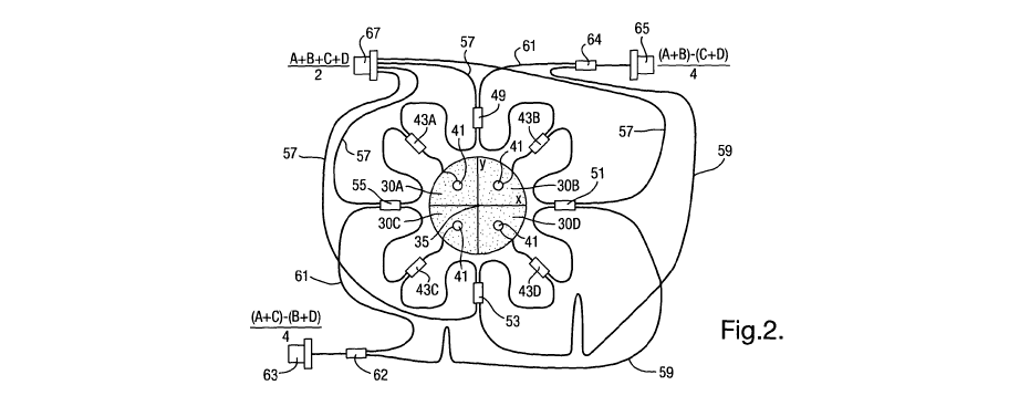
In Figure 2 the four photodetectors 39 each are replaced by a respective
optical fibre or waveguide 41. The end of each optical fibre is disposed in
the
plane of the photodetector it replaces so as to receive light reflected to it
from
the respective surface 30A-D. Each optical fibre 41 is of the same optical
length and leads to a respective 50/50 splitter/combiner 43 A-D where it is
divided into two parts. Each part of the split signal is taken by an optical
fibre
45 to one of four further 50/50 splitter/combiners 49, 51, 53, 55, where it is
combined with a similarly-split signal from the splitter 43 of an adjacent
quadrant. Again the optical fibres 45 are of equal optical length. The
splitter/combiners 49 and 51 each provide two equal outputs to respective
optical fibres 57 and either 59 or 61, It can be seen that the outputs from
the
splitter/combiners 49, 51, 53, 55 (and thus the inputs to optical fibres 57,
59, 61)
are respectively (A+B)/4, (B+D)/4, (C+D)/4 and (A+C)/4, where A, B, C and D
are the signals originating from quadrants 30A-D respectively. These signals
are in phase with each other at the modulation frequency.
The optical fibre 59 from splitter/combiner 51 and the optical fibre 61
from splitter/combiner 55 are taken via a combiner 62 to an azimuth
photodetector 63. The optical fibre 59 from splitter combiner 53 and the
optical
fibre 61 from splitter /combiner 49 are taken via a combiner 64 to an
elevation
photodetector 65.
The optical fibres 59 are of equal optical length, and are X /2 longer than
the optical fibres 61 (which also are of equal optical length), where ,, is
the
modulation wavelength of the signal. The additional optical length of X/2
delays the light signals passing through the fibres 59 by an amount,
equivalent
CA 02789265 2012-08-08
WO 2011/098784 PCT/GB2011/050183
-7-
to a phase-shift of 1800. This effectively reverses the algebraic sign of the
signals in fibres 59, and so the combined signals delivered from combiners 62,
64 to detectors 63, 65 are
(A+C)-(B+D) and (A+B)-(C+D)
4 4
i.e. the azimuthal and elevational components of the direction of
incidence of the light signal on the detector, relative to x and y axes
centred on
the detector boresight 35 as shown in Figure 2.
Thus the optical signals delivered to the photodetectors 63, 65 already
have been processed to yield azimuth and elevation signals, and require
further
processing only as necessary for the particular application for which the
apparatus is intended to be used.
The optical fibres 57 are all of the same length and are significantly
shorter than both the fibres 59 and 61. They deliver an in-phase sum signal
(A+B+C+D)/2 to a photodetector 67. This signal provides an indication of the
amplitude (brightness) of the incident light signal, and can be utilised to
normalise (scale) the outputs of the photodetectors 63, 65. It will be
appreciated that it is the relative values of the outputs of photodetectors
63, 65
which are of interest, and not their absolute values. The output of
photodetector
67 also can be utilised for controlling the gain of circuitry to which the
outputs of
photodetectors 63, 65 are supplied. This can be useful when the incoming
signal is weak, or alternatively when is too strong, as may be the case for
the
terminal phase of the flight of a laser-guided munition to its target. For
example,
the apparatus may comprise an adjustable gain control circuit, the circuit
being
arranged so that the gain of the photodetectors 63, 65 is adjusted according
to
the amplitude,. Thus, if the signal amplitude is too large, the adjustable
gain
control circuit may be adjusted to attenuate the signal from the
photodetectors
63, 65. Alternatively, the signal may be switched to a different, less
sensitive,
photodetector, or to a separate lower-gain amplifier, or to an optical or
other
attenuator, if the detectors 63, 65 otherwise would be saturated. Similarly,
if the
amplitude is too small, the adjustable gain control circuit may be adjusted to
boost the signal from the detectors 63, 65. Alternatively, the signal may be
switched to a different, more sensitive, photodetector, or to a separate,
higher-
CA 02789265 2012-08-08
WO 2011/098784 PCT/GB2011/050183
-8-
gain amplifier. In yet another alternative, the gain adjustments may be
achieved
by operating on the light signals before they reach the detectors 63, 65, 67,
for
example by switching-in in-line fibre attenuators or amplifiers as required.
This
can have the advantage of being simpler to implement than gain control during
electrical signal processing.
In the described embodiment, the waveguides are in the form of optical
fibres. Optical fibres have the advantage that they are generally relatively
cheap, and are available in very long lengths. Either a single fibre or a
bundle
of fibres (preferably jacketed) may be used. When a bundle of fibres is used,
the fibres may advantageously be distributed so as that each views a
respective
different part of the surface of the quadrant 30A, B, C or D. The fibres from
each quadrant are brought together before the splitter 43A, B, C or D so as to
provide a single signal to it. Jacketed optical fibres can be relatively
bulky, and
in some embodiments alternatives, for example planar waveguides, may be
used.
Whilst the present invention has been described and illustrated with
reference to particular embodiments, it will be appreciated by those of
ordinary
skill in the art that the invention lends itself to many different variations
not
specifically illustrated herein.
For example, a further improvement in resolution can be achieved by
sub-dividing each quadrant into further sub-quadrants, and applying the
invention to those sub-quadrants. However, this refinement will require
significantly more complex signal processing.
Where in the foregoing description, integers or elements are mentioned
which have known, obvious or foreseeable equivalents, then such equivalents
are herein incorporated as if individually set forth. Reference should be made
to the claims for determining the true scope of the present invention, which
should be construed so as to encompass any such equivalents. It will also be
appreciated by the reader that integers or features of the invention that are
described as preferable, advantageous, convenient or the like are optional and
do not limit the scope of the independent claims. Moreover, it is to be
CA 02789265 2012-08-08
WO 2011/098784 PCT/GB2011/050183
-9-
understood that such optional integers or features, whilst of possible benefit
in
some embodiments of the invention, may be absent in other embodiments.