Note: Descriptions are shown in the official language in which they were submitted.
CA 02789672 2012-08-13
WO 2011/100068 PCT/US2011/000263
1
HERMETIC PACKAGE WITH LEADED FEEDTHROUGHS FOR IN-LINE
FIBER OPTIC DEVICES AND METHOD OF MAKING
[0001] FIELD OF THE INVENTION
[0002] This invention relates to hermetic packaging
for fiber optic devices, and particularly to a leaded
package for in-line fiber optic devices that provides
electrical feedthroughs compatible with batch
processing using micromachined silicon wafers.
[0003] BACKGROUND OF THE INVENTION
[0004] Fiber optic devices present special
challenges to a package designer beyond those
encountered with standard electronic packaging. Of
particular concern to fiber optics designers are
optical feedthroughs that provide optical communication
between optical elements inside a package and elements
outside of the package. Often such optical
feedthroughs use one or more optical fibers that must
be reliably secured to the package and at the same time
hermetically sealed to prevent ingress of atmospheric
moisture that can adversely affect long-term
reliability of optical elements inside.
[0005] In addition, fiber optic devices often
require electrical feedthroughs to allow electrical
signals to pass to and from electronic elements within
the package. Such electrical feedthroughs are subject
to the same requirements of reliability and hermeticity
as optical feedthroughs. However, electrical
CA 02789672 2012-08-13
WO 2011/100068 PCT/US2011/000263
2
feedthroughs often have many different processing
requirements in manufacturing than optical feedthroughs
due to differing materials and process temperatures.
As such, accommodating both in a manufacturing
environment presents a challenge to the fiber optics
package designer, in addition to the challenges of
achieving ever smaller, lower cost packages.
[0006] The term "hermetic" as used herein, indicates
impermeability of an enclosed structure to air ingress.
However, all enclosed structures are permeable to some
degree. Hence, for the purpose of clarity, the term
hermetic is used hereinafter to indicate a permeability
expressed as a measured helium flow rate into the
enclosure of less than 5x10⁻⁸ atm-cc/sec, a limit often
used with optoelectronic devices.
[0007] An in-line fiber optic device, that. is where
light passes into and out of the package by way of a
single, continuous optical fiber, present still further
challenges. Examples of in-line devices are the
optical fiber taps described in U.S. Pats.
No. 6,535,671 (issued to Craig D. Poole on March 18,
2003) and 7,116,870 (issued to Craig D. Poole on
October 3, 2006), in which a structure is formed
directly in midsection of the fiber causing light to be
ejected ("tapped") out of the side of the fiber. In
such devices, the well-known method of hermetically
sealing a glass fiber by inserting a fiber end into a
ferrule that forms a seal around the fiber as
described, for example, in U.S. Patent No. 5,692,086,
CA 02789672 2012-08-13
WO 2011/100068 PCT/US2011/000263
3
is not applicable owing to the lack of a terminal fiber
end with which to work.
[0008] The `671 Poole patent describes a method for
hermetically sealing an in-line fiber optic tap inside
a housing containing a photodiode by threading the
optical fiber through a narrow tube that is then sealed
using sealing glass placed between the fiber and tube
walls. Since tube diameter must be kept small to
minimize stress on the fiber, this method suffers from
a need to thread long lengths of optical fiber through
narrow tubes when such fiber lengths may exceed 2
meters, consequently rendering this approach
impractical for low cost manufacturing.
[0009] In order to hermetically seal in-line fiber
optic devices, one is thus led to consider a "sandwich"
geometry in which two parts are brought together to
form a seal around the fiber using some type of sealing
material. An example of such an approach is described,
in U.S. Pat. 6,074,104 (issued to Kimikazu Higashikawa
on June 13, 2001) There, a single fiber end is sealed
inside a hermetic cavity by sandwiching the fiber
between a metal case and metal seal cover using low-
temperature glass solder and a resin as the sealing
medium.
[0010] In addition to providing optical
feedthroughs, both the `671 Poole and `104 Higashikawa
patents describe packages that include electrical
feedthroughs that are connected to leads for mounting
the finished packages directly to electronic printed
CA 02789672 2012-08-13
WO 2011/100068 PCT/US2011/000263
4
circuit boards. However, both approaches suffer from
the use of conventional TO can, DIP or surface-mount
electronic packaging that do not lend themselves
readily to batch processing methods and require
numerous process steps to form the leaded package prior
to the sealing,of the optical fiber. These approaches
are difficult to manufacture at low cost.
[0011] Therefore, a need currently exists in the art
for a hermetic package for in-line fiber optic devices
that includes both optical and electrical feedthroughs,
is compatible with batch processing techniques using
micromachined silicon wafers and advantageously
remedies the above-described deficiencies in the art.
[0012] SUMMARY OF THE INVENTION
[0013] The present invention satisfies this need by
using a single metal lead structure that is
hermetically mounted to a silicon substrate and
provides electrical communication with electronic
elements inside a sealed cavity, the cavity having been
formed by the silicon substrate and a separate silicon
sealing cap, through holes etched into the silicon
substrate. The metal lead structure has a
cylindrically shaped protrusion that extends into the
sealed cavity through vertical holes etched in the
silicon substrate using deep-reactive ion etching
(DRIE). The electrical feedthrough thus formed is
sealed using low-temperature sealing glass.
CA 02789672 2012-08-13
WO 2011/100068 PCT/US2011/000263
[0014] Advantageously, the silicon substrate and
sealing cap have complimentary grooves formed therein
for hermetically sealing a glass fiber for optical
communication with elements within the sealed cavity.
5
[0015] The sealed structure thus formed is further
enclosed in a two-piece metal shroud to provide
structural support to the sealed structure as well as
shielding from electrical noise. The result is a
leaded package that can be mounted directly onto a
printed circuit board.
[0016] In the preferred embodiment of the invention,
the package forms an in-line power monitor in which the
sealed cavity contains a photodiode that is
electrically connected to electrical leads that are in
optical communication with an optical fiber such that
the electrical current carried by the leads is
proportional to the optical power carried by the fiber.
[0017] The preferred embodiment further includes
spacer beads added to the glass matrix to seal the
electrical feedthrough so as to control the spacing
between the silicon substrate and the lead structure
and thereby control electrical capacitance of the
package.
[0018] Further, the present inventions teachings
extend to a batch process for manufacturing leaded
packages using micromachined silicon wafers. The batch
process utilizes screen printing techniques to apply
glass solder paste on a wafer followed by thermal
CA 02789672 2012-08-13
WO 2011/100068 PCT/US2011/000263
6
treatment to burn-out residual organics and glaze the
sealing glass. Electrical leads are attached to form
hermetic electrical feedthroughs in the silicon wafer
prior to dicing the wafer into individual parts. In
this way many parts are processed together, thus
greatly increasing throughput and lowering its cost.
[0019] BRIEF DESCRIPTION OF THE DRAWINGS
[0020] The teachings of the present invention can be
readily understood by considering the following
detailed description in conjunction with the
accompanying drawings in which:
[0021] FIG. 1 shows a perspective exploded view of
leaded package 100;
[0022] FIG. 2 shows a cross-sectional view of a
conventional embodiment of leaded package 100 depicted
in FIG. 1 the cross-section being taken along a plane
indicated by the dashed box in the latter figure;
[0023] FIG. 3 shows a cross-sectional view of an
embodiment of leaded package 100 depicted in FIG. 1 and
according to the present invention, the cross-section
being taken in the same manner as for FIG. 2;
[0024] FIG. 4 shows a bottom surface of a silicon
wafer having an etched pattern according to the present
invention;
CA 02789672 2012-08-13
WO 2011/100068 PCT/US2011/000263
7
[0025] FIG. 5 shows a perspective view of a lead
mounting apparatus according to the present invention;
and
[0026] FIG. 6 is a perspective view of a top surface
of a silicon wafer having etched pattern and electrical
leads attached according to the present invention.
[0027] To facilitate reader understanding, identical
reference numerals are used to denote identical or
similar elements that are common to the figures. It is
understood that the figures are not drawn to scale.
[0028] DETAILED DESCRIPTION OF THE PREFERRED
EMBODIMENT
[0029] Before describing the interactive hermetic
package, to enhance reader understanding, a
conventional package for an in-line fiber optic tap
will be explained in conjunction with reference to
FIGs. 1 and 2.
[0030] Referring to the drawings, FIG. 1 shows a
perspective view of leaded package 100 having silicon
substrate 102, silicon sealing cap 104, optical
fiber 106, optical fiber tap 108, and photodiode 110.
Photodiode 110 is mounted at the bottom of well 112
that has been formed in silicon substrate 102 using
anisotropic wet etching.
[0031] Glass solder 114 and 116, and grooves 118 and
120 in silicon substrate 102 and sealing cap 104,
respectively, form a hermetically sealed cavity,
CA 02789672 2012-08-13
WO 2011/100068 PCT/US2011/000263
8
enclosing optical fiber tap 108, photodiode 110 and
well 112, when cap 104 and substrate 102 are brought
together under appropriate temperature and pressure so
as to cause glass solder 114 and 116 to flow and form a
continuous seal.
[0032] Prior to sealing, optical fiber tap 108 is
positioned above photodiode 110 so that light ejected
out of tap 108 efficiently illuminates photodiode 110.
[0033] Photocurrent generated by photodiode 110 is
carried by leads 122 and 124 which are connected to
cathode and anode of photodiode 110, respectively,
using protrusions 126 and 128 formed at top of
leads 122 and 124. Lead 122 with protrusion 126 and
lead 124 with protrusion 128, can each be formed from a
single piece of metal, such as "Kovar" material
("Kovar" is a registered trademark of Carpenter
Technology Corporation), in a stamping operation.
Protrusions 126 and 128 extend up through holes etched
through bottom of well 112 and are secured to the
bottom of substrate 102 using low-temperature sealing
glass 130. A more detailed description of the
electrical feedthroughs is provided below.
[0034] After sealing, the structure comprising
silicon substrate 102, silicon sealing cap 104, and
attached leads 122 and 124 is secured to bottom metal
shroud 132 using epoxy 136 and subsequently enclosed by
adding metal shroud cover 134. Metal shroud cover 134
and bottom metal shroud 132 provide electrical
shielding for the enclosed elements in addition to
CA 02789672 2012-08-13
WO 2011/100068 PCT/US2011/000263
9
providing mechanical support and protection for
handling.
[0035] FIG. 2 shows in cross-section a conventional
embodiment of leaded package 100 depicted in FIG. 1,
with metal shroud cover 134 and bottom metal shroud 132
removed. As noted, the cross-section (as is the case
also for FIG. 3) is taken along a plane indicated by
the dashed box in FIG. 1. In this embodiment, optical
fiber tap 108 is formed in fiber 106 prior to assembly
using methods described in the `870 Poole patent.
Electrical communication between photodiode 110 and
leads 122 and 124 is provided by protrusions 126 and
128 which extend upward through etched holes 202 and
204. Both center well 112 and etched holes 202 and 204
are formed using anisotropic wet etching in a two-step
process in which center well 112 is etched first,
followed by etched holes 202 and 204 in a secondary
etch step. Both center well 112 and etched holes 202
and 204 are substantially square in shape with sloping
side walls angled at 54.7 degrees as a result of the
anisotropic etching process preferred in single-crystal
silicon. Protrusions 126 and 128 have a conical shape
with side angles matched to complement those at the
sloping walls of etched holes 202 and 204 so as to
provide a uniform gap between protrusions 126 and 128
and the wall surfaces of holes 202 and 204. To form a
hermetic seal, this gap is filled with low-temperature
sealing glass 130. Preferably, sealing glass 130 will
be chosen to have a higher melting temperature than
glass solder 114 and 116 in order to maintain
CA 02789672 2012-08-13
WO 2011/100068 PCT/US2011/000263
structural integrity when forming the seal between
silicon cap 104 and substrate 102.
[0036] Photodiode 110 is connected to
5 protrusions 126 and 128, using conductive epoxy 206 and
wire-bond wire 208. Alternatively, a eutectic solder
compound such as 80/20 Gold/Tin solder can be used in
place of conductive epoxy 206. In order to avoid
electrical shorting of protrusions 126 and 128 and
.10 photodiode 110 to silicon substrate 102, the surfaces
of silicon substrate 102 are coated with an insulating
layer of oxide (SiO2) (not shown but well known) prior
to assembly.
[0037] The conventional electrical feedthroughs
shown in FIG. 2 suffer from several problems:
[0038] (1) The anisotropic wet etch process
necessarily leads to square-shaped
through-holes, due to the crystalline
structure of the silicon. Such holes
have sharp corners that focus stresses
causing diminished reliability of the
seals.
[0039] (2) The sloping walls, angled at 54.7
degrees of etched holes 202 and 204, and
center well 112 result in the formation
of knife edge 210 where etched holes 202
and 204 enter center well 112. This
knife edge and others similarly formed
are delicate and have a tendency to
crack causing the protective oxide
coating to separate from substrate 102
CA 02789672 2012-08-13
WO 2011/100068 PCT/US2011/000263
11
thus shorting the metal leads 122 and
124 to the bulk silicon of
substrate 102.
[0040] (3) The capacitance of the package is not
well controlled due to variability of
the glass seal spacing, d, between the
metal lead structure and the silicon
substrate and which is created when
leads 122 and 124 are attached to
substrate 102.
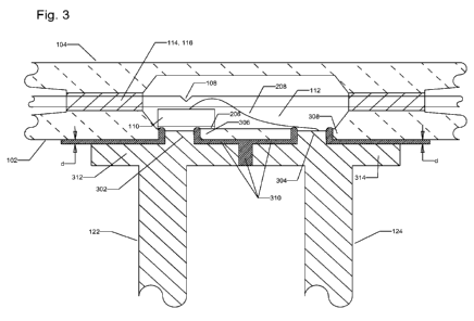
[0041] FIG. 3 shows, in cross-section, leaded
package 100, with a detailed depiction of improved
electrical feedthroughs according to the present
invention. Electrical communication between
photodiode 110 and leads 122 and 124 is provided by
protrusions 302 and 304 which extend upward through
etched holes 306 and 308. Center well 112 is formed
using anisotropic wet etching, with sloping side walls
angled at 54.7 degrees again owing to the anisotropic
etching process in single-crystal silicon. Etched
holes 306 and 308 in silicon substrate 102 are formed
using deep-reactive ion etching (DRIE) in a secondary
etch step. Etched holes 306 and 308 are cylindrical in
shape with a side wall slope of less than 2 degrees.
Leads 122 and 124 have protrusions 302 and 304 that
have a cylindrical shape with vertical side walls (less
than 2 degrees side-wall slope) and a maximum 0.002"
(approximately .0051 cm) radius of curvature at the
base of the protrusion and can be formed from a single
piece of metal, such as Kovar material, in a stamping
operation. The diameter of protrusions 302 and 304 is
CA 02789672 2012-08-13
WO 2011/100068 PCT/US2011/000263
12
such as to provide a uniform gap between the
protrusions and the wall surfaces of holes 306 and 308.
Preferably, the diameter of the cylindrical protrusion
is nominally 0.012" (approximately .0305 cm). To form
a hermetic seal, the gap between protrusions 302 and
304 and between lead structure 312 and 314 and silicon
substrate 102 is filled with low-temperature sealing
glass 310. Such a long glass-seal path length provides
for a hermetic seal and robust mechanical attachment of
leads 122 and 124 to silicon substrate 102. Sealing
glass 310 contains spacer beads in its glass matrix to
control the glass seal spacing, d, between silicon 102
and lead structures 312 and 314 and thereby control the
electrical capacitance of the package. Preferably,
spacer beads consist of borosilicate glass having a
nominal bead diameter of 0.002" (approximately
.0051 cm). Spacer beads are added to the glass solder
paste in concentrations less than 0.4wt%. In addition,
sealing glass 310 will be chosen to have a higher
melting temperature than glass solder 114 and 116 in
order to maintain structural integrity when forming the
seal between silicon cap 104 and substrate 102.
[00421 Photodiode 110 is connected to
protrusions 302 and 304, using conductive epoxy 206 and
wire bond wire 208. Alternatively, a eutectic solder
compound such as 80/20 Gold/Tin solder can be used in
place of conductive epoxy 206. In order to avoid
electrical shorting of protrusions 302 and 304 and
photodiode 110 to silicon substrate 102, the surfaces
of silicon substrate 102 are coated with an insulating
layer of oxide (Si02) prior to assembly.
CA 02789672 2012-08-13
WO 2011/100068 PCT/US2011/000263
13
[0043] FIG. 4 shows a 100mm (approximately 4")
micromachined silicon wafer 402 comprised of an array
of silicon substrates 102 that have low-temperature
sealing glass 310, on its back surface, around
holes 302 and 304. Batch processing of silicon
wafer 402 is achieved by an anisotropic wet etching of
the front surface of the wafer followed by DRIE
processing to form holes 302 and 304 on the back
surface. Low-temperature sealing glass 310 is applied
to the back surface of the wafer around holes 302 and
304 for electrical lead attachment. Preferably, glass
solder paste is applied to the wafer using a screen
printing process which allows precision placement of
the glass solder paste around holes 302 and 304 in a
figure-8 pattern followed by thermal treatment to
burn-out residual organics and glaze sealing glass 310
in preparation for electrical lead attachment. A
double layer screen printing process of the glass
solder paste is advantageously used to provide precise
control of both thickness of the glass solder paste and
its placement around holes 302 and 304.
[0044] Although a 100mm silicon wafer is used in the
preferred embodiment, increasing the silicon wafer size
to 150mm (approximately 6") or 200mm (approximately 8")
significantly increases the number of parts that can be
produced from a single wafer.
[0045] FIG. 5 shows a fixture that has been
developed to attach electrical leads 122 and 124 to
wafer 402 with low-temperature sealing glass 310 around
CA 02789672 2012-08-13
WO 2011/100068 PCT/US2011/000263
14
holes 302 and 304. Prior to placement of the leads,
wafer 402 is loaded onto vacuum fixture 502. Vacuum
fixture 502 supports wafer 402 and mobile carrier 504
while providing suction to both in order to maximize
stabilization during placement of the leads. Comb
fixture 506 is supported by separate support arms 508
which move comb fixture 506 relative to wafer 402.
Comb fixture 506 has slots 510 precisely machined at
regular intervals matching feedthrough hole spacing in
wafer 402. With the vacuum turned on, vacuum
fixture 502 provides suction through holes 302 and 304
in wafer 402 such that when electrical leads 122 and
124 are placed in position with cylindrical
protrusions 302 and 304 in holes 306 and 308, the
suction is sufficient to hold the electrical leads in
place. An entire row of electrical leads can be
properly positioned while the vacuum holds them in
place after which comb fixture 506 is advanced by means
of support arms 508. Upon advancing comb fixture 506,
the leads that have been placed enter into slots 510
where they are enclosed and protected from
dislodgement. Vacuum fixture 502, mobile carrier 504,
comb fixture 506 and support arms 508 are designed to
have appropriate characteristics to allow for precise
parallel alignment between slots 510, leads 122 and 124
and wafer 402. After advancing comb fixture 506, a
next row of electrical leads can be applied and the
process repeated, and so forth. After all the leads
are placed over their corresponding holes, comb
fixture 506 is lowered by support arms 508 until the
entire weight of comb fixture 506 is pressing down on
electrical lead structures 312 and 314. The vacuum is
CA 02789672 2012-08-13
WO 2011/100068 PCT/US2011/000263
then turned off and lead protrusions 302 and 304
positioned in holes 306 and 308, are held in place by a
force provided by comb fixture 506 and applied through
comb teeth 512 onto lead structures 312 and 314.
5
[0046] Support arms 508 are then used to transport
mobile carrier 504, wafer 402, comb fixture 506 and
electrical leads 122 and 124, onto a heat source such
as a hot plate where the entire assembly is heated to
10 the seal temperature of sealing glass 310. Preferably,
this temperature causes sealing glass 310 to flow
around protrusions 302 and 304 on the electrical leads
to fill the space between the protrusions and hole
walls 302 and 304 and the space between lead
15 structure 312 and 314 and silicon 102 forming a
hermetic seal between the electrical feedthrough and
the silicon substrate. Seal thickness, d, between lead
structure 312 and 314 is controlled across the wafer by
the presence of spacer beads in sealing glass 310 and
the force applied by comb fixture 506 thereby
controlling the electrical capacitance of the package.
[0047] Because of the high-temperature process
involved in attaching leads 122 and 124 to wafer 402,
comb fixture 506 should be made of a high-temperature
material that is also thermally insulating so as to
minimize heat conduction away from silicon wafer 402
and leads 122 and 124 during sealing. An example of
such a material is "Macor" machineable ceramic
manufactured by Corning Glass Works Corporation
("Macor" is a registered trademark of Corning Glass
Works Corporation). Mobile carrier 504 on the other
CA 02789672 2012-08-13
WO 2011/100068 PCT/US2011/000263
16
hand should be made of a thermally conductive material
such as aluminum nitride so as to efficiently deliver
heat to the entire assembly for sealing.
[0048] After attaching leads 122 and 124 to the back
surface of wafer 402, low-temperature sealing glass 114
is applied to the front surface of wafer 402 around
etched well 112, as shown in FIG. 6. Following lead
attachment to the backsurface of wafer 402, the wafer
is placed on a new mobile carrier designed to
accommodate the leads while glass solder paste is
screen printed to the front surface of the wafer. This
glass solder paste is applied in a race-track pattern
around well 112 (see FIGs. 1 and 3) such that
groove 118 is also filled with this paste, followed by
thermal treatment to burn-out residual organics and
glaze sealing glass 114 in preparation for hermetic
sealing of silicon cap 104 to substrate 102. The
amount of glass solder paste deposited in groove 118 is
adjusted by varying the design of the screen used in
printing, and by using a double-layer screen printing
process. In the preferred embodiment, the race-track
pattern of the screen is slightly tapered at a location
at groove 118 to alter the amount of glass solder paste
that is deposited. The quantity of sealing glass in
groove 118 should be sufficient to form a continuous
hermetic seal around optical fiber 106 when silicon
cap 104 is sealed to substrate 102, but not in excess
to impact the optical performance of the device,
preferably, sealing glass 114 will be chosen to have a
lower melting temperature than sealing glass 310 in
order to maintain structural integrity of the leads
CA 02789672 2012-08-13
WO 2011/100068 PCT/US2011/000263
17
when forming the seal between silicon cap 104 and
substrate 102.
[0049] Finally, finished parts are separated from
the wafer by dicing. Water is commonly used as a
cutting lubricant/coolant during the dicing process.
However, low-temperature sealing glass such as those
used here is subject to reaction with water during
wafer dicing with a diamond saw. In particular,
degradation of sealing glass 114 during the dicing
process could result in poor sealing of silicon cap 104
to silicon substrate 102 thereby compromising optical
performance and hermeticity of the package. Addition
of a cutting lubricant, such as L300 offered by UDM
Systems of Raleigh, NC, to the water supply for dicing
renders the water less reactive with the sealing glass
than would otherwise occur.
[0050] Advantageously, the present invention
provides a highly reliable hermetic package for in-line
fiber optic devices that can be cost-effectively
manufactured using wafer-level processing of
micromachined silicon and batch processing techniques.
[0051] Clearly, those skilled in the art can readily
modify the inventive teachings. In that regard,
alternative embodiments could use UV laser cutting
techniques to form the vertical wall holes in the
silicon substrate. Alternatively, glass solder paste
could be applied on the wafer-level using robot
dispensing of the material, however dispensing
techniques would increase wafer processing time and
CA 02789672 2012-08-13
WO 2011/100068 PCT/US2011/000263
18
precision placement of the paste around the feedthrough
holes would be difficult to maintain across the wafer.
In addition, the scale of wafer-level processing could
be increased by using larger silicon wafers (e.g.,
150mm or 200mm diameter approximately 6 and 8" cm,
respectively), thereby dramatically increasing the
number of individual parts per wafer. Also,
alternative embodiments could protect the sealing glass
during the dicing operation of the individual parts
through use of alternative methods than use of a
cutting lubricant, such as application of a protective
coating over the sealing glass prior to dicing followed
by. removal of the coating after dicing.
[0052] Although various embodiments which
incorporate the teachings of the present invention have
been shown and described in detail herein, those
skilled in the art can readily devise many other
embodiments that still utilize these teachings.