Note: Descriptions are shown in the official language in which they were submitted.
CA 02789705 2012-08-13
WO 2011/100738 PCT/US2011/024864
SINGLE PHASE MULTILEVEL INVERTER
CROSS REFERENCE TO RELATED APPLICATIONS
[0001] This application claims the benefit of U.S. Provisional
Application No. 61/304,538, filed February 15, 2010, the
disclosure which is incorporated herein by reference in its
entirety.
BACKGROUND OF THE INVENTION
[0002] The invention relates generally to DC to ac inverters.
More specifically, the invention rel..,.es to methods and
systems ver. topology.
Ys t= for multilevel } ~:11eJel inverters having `ivhaving a simplified
~.[0003] Today, the power industry ~ has revived and entered a new
age using renewable energy, and high efficiency power
generation, transmission and distribution where multilevel
power converters can assume e significant ._ e
~._._ t, or.lflc ro 1:1 s.
[0004] Multilevel power converters emerged from the
r_eali.zat:.on that single power semiconductors cannot meet the
voltage requirements for medium voltage l.tage r~-~au_rnts ~ required medium
~_tach~ power
conversion. Multilevel power conversion has rapidly grown in
the field of power engineering for the applications of medium
voltage ac drive, AC '''z.. .~:s ~,n ass .l. _ e,, Flexible System (FACTS)
devices, Medium Voltage .'' DC (MVDC) transmiss ion, and High
t High
Voltage DC (HVDQ transmission systems. -.yes: :.te toda.y' s high
power semiconductor technology that has reached 6.5 k\,' and 2.5
kA power ratings, multilevel power converte:_s built with
mature medium power semiconductor cr~. technology present
alternative solutions with many advantages over
competitive
conventional 2--level. converters due to their 910-J-1-1-ity to
synthes ize waveforms exhibiting lower distortion and better
harmonic cancellation, smaller ----- and common-mode voltage, and
dt
CA 02789705 2012-08-13
WO 2011/100738 PCT/US2011/024864
low switching frequency operation, and. attain higher voltages
using semiconductor devices ;n;_~'t.l? ATIa_L1 er voltage L ._ ~ Jratings.
Topologically, ~ ' a multilevel structure can be considered
~. an ac voltage synthesizer _sl.zer realized from mul-t -;~1e dis~t~.
voltage discrete
voltage sources. Multi. .-e, equal sources are required.
Multilevel inverters provide an ac output waveform at discrete
voltage levels. The more ~` steps r levels 'n~~E_.~_.~ e a. smoother
si.nusoidal waveform and reduce the amount of output filtering.
Practically, it is a trade-off to select the _.,.m per of -levels
considering the converter complexity and filter requirements.
By optimizing the angles and heights of steps, certain -lower
order harmonics can be cancelled. IIn addition, he harmonics
:.._ - t spectrum can be reduced by using Pulse Width. _--a; -:,n (PUV. 4
using . Modulation ~)
techniques at each level.
[0006] Numerous multilevel inverter topologies have been
proposed and studied for power utility and motor drive
applications. ,=IG5. 1A and _..:B show prior art half---bridge and
full--bridge diode--clamped or neutral---point--c:-amped (NBC)
inverters. _-IGs2A and 2B show prior art :-f_ b idg and
full-bridge capacitor-clamped or flying-capacitor inverters.
FIG. 3 shows a prior art cascaded H--bridge inverter with
separate do supplies and an ac output at nodes .= and B. FIG.
4 shows a prior art topology that replaces an H. -bridge
architecture with cascaded 2--terminal submod~._.-es without
separate do sources to form a modular structure.
[0007] The diode-clamped multilevel converter is the most
widely used inverter topology. However, this topology is
cumbersome to implement for levels bfive.
beyond
2
CA 02789705 2012-08-13
WO 2011/100738 PCT/US2011/024864
[0008] There is a need for a simplified inverter topology that
allows for levels greater than five.
]=^v`T J... _<<}:iQ
ti TIVI IARY OF THE
[0009] The inventors have discovered that _- would be
desirable to have methods and systems for multilevel inverters
.,1_
using -
having a plurality of levels .s la simplified topology. - ~o gy, For
single phase systems, embodiments provide a
topology using unidirectional and bidirectional contr0I._I_E!d
switching interconnections. Since the ac output is obtained
differentially, the required amount of DC sources can be
reduced by half.
[0010] Embodiments provide a class of sing phase multilevel
inverter topologies using a f,.-,,.!I-bridge approach with
bidirectional interconnections. Compared i' , p e'd or
flying-capacitor multilevel topologies, the required
split-rail s a.e _.~~ss -equ1_ _r edpower idc inputs are , and the ... .;
switch
number can b e ed by emov ng r_ed?ndant w:.t'ch:_n _'=
With asymmetrical sources, the number of output Ievel.s may
be increased in the proposed generalized multilevel structure.
[0011] One aspect of the invention provides a method for a
single phase inverter topology. Methods according to this
aspect of the invention comprise selecting a number of desired
inverter output levels n , where in =- 5 , is an integer and an
odd num oer, determining a number of equal DC sources n, where
in --- 1
H= , coupling the n DC sources _..n ser_ ies, wherein
the
2
source 1''-1 t : a positive
rCseries has has - :~ first DC ~ source that defines 4. node P and a last DC
source that defines a negative node N,
defining one or more source series nodes between each DC.
source the source series wherein the source series, node
CA 02789705 2012-08-13
WO 2011/100738 PCT/US2011/024864
after tale first. DC source that defines a positive node P is
the first source series node and the source series node before
the last DC source that defines a negative node N is ,.he 1...,t
source se lies node, deterITinin Y number o nidire reg=ional
controlled switches Uf~:S , assembling one or Ii1C:re 1r1~~e
cells, wher'e' n an inverter cell comprises six unidi rec:.ional
ues
^ he
C' rt1'_'C11_ed s tcbc ano s ~1 6 `E' no
number of inverter cells 1 ? enui red for{ she selected number of
inverter ou _put_ levels in , arranging four Of the
unidirectional controlled switches for each cell as
wo bidirectional cunt rolleC : 5';'ch o each inveruer cell
i
coupling two bidirectional controlled switches together
formirlq a cell series node and, couplinq the other terminal of
each bidirect--ional controlled switch to the emitter terminal
of one unidirectional cc;ntro_led switch forming two cell
n'o;des, coup- the ce11 series node,, o f a {cell to the irst.. '..i I.I .~(õf-
_~-. cries node and cou~~./l_n\J the ~..'.J11ec I~O- i., l_-L!I.~nals '.J Pt
!l~e
cit , ~ 7 s j-- node ,.11 . two I:Iriidir~-~.~:io:ial controlled .~, itche .~
t c; 7= .e] nods. or each -ema~ning1 inverter cell, coupling the cell series
node to a following source series node and coupling each
unidirectional contrc;lied swit'ch's collector terminal to
respective cell node o-` a previous inverter cell, and coupling
the emitter terminal for each of the two remaii_
unid-i-rect1_ona controlleU. " Switches to the :Mode N and coupling
the each co_lei t r al to a respective cell node of the
last inverter cell.
[0012] Another aspect_ of the invention _õ a single phase
inverter topology method. Methods according to this aspect of
the invention comprise selecting a number of desired inverter'
output levels in , where m'_-w>5, _,s an inueger and an odd number,
:jetermin1_ng =. number o f eoua .. DC sour c:et l .,Isle:-e, n _
4
CA 02789705 2012-08-13
WO 2011/100738 PCT/US2011/024864
coupling the n DC sources in se.-.-J-es, wherein the source series
has a st DC source that def__nes a positive node P and a
last, D'r- SO,.irce ttlri;= defines a negative node N , defy__lI.q one
or more source series nodes bet_S','een each DC source in she
Source se-_e` wherein the source series node after the first
DC source t1=4.,= defines a pos_t_ve node P is the fir - source
series node and the source se-_e` node b e f o e the lass DC
sou-ice that defines a negative node ' is the last source
serif--,s node, determini i a number of- unidirectional controlled
switches nes , assembling- one or il'c : e iverter cell ,, wherein
an inverter cell comprises ~~uY:_directic;na_ controlled
ties
switches and the quotient of 6 determines the number of
inverter cells required for the selected numbe- of Inverter
output lev-els in arranging four of the unidirectional
controlled switches for eaci".. inverter cell as two
bidi--f::ctio al controlled switches, f or each 1' n ter ceDll,
coupling two bidirectional controlled switches together
f: riling a cell series node and coupling the ot'-hie- terminal c
each bidirectiJnal controlled switch to the emitter terminal
of one unidirectional cc;ntro_led switch forming two cell
nodes, co-u ;lin the cell :series nod f a f} -St Inverter cell
O the last source series node and coupling i ^e emitter
rmina_ for each O the two -eiilainino unidirectional
ant:-7_ _ .eci ..,. w to the ' nog 2 N and coup 11 tg each O._- cto
. -i he e
terming to respective cell node of the t I: %erter cell,
fa:. each ema.:_ning inT-;eerte ce-_- , coupling th.e ceseries
node to g 7rev J. n us source se-c?-es nude and coup1_G; each Ce ll
node to a tin d I E 7_c;na.7_ cunt O ---e'd switch' collector
terming :. of fol.lowin inverter cell, and for the last
inverter -el - , coupling the O._ ector to m7_I:,q ..s of the last
cfe11` s two unidirectional contr_olle'd switches to the node P
CA 02789705 2012-08-13
WO 2011/100738 PCT/US2011/024864
[0013] The details of one or more embodiments of the invention
are set forth in the accompanying drawings and the description
below. Other features, objects, and advantages of the
invention will beapparent from the description and drawings,
and from the claims.
BRIEF DESCRIPTION OF THE DRAWINGS
[0014] FIG. 1A is a prior art half-bridge diode-clamped
5-level inverter topology.
[0015] FIG. 1_B is a prior art aul-:J_-bridge diode-clamped
5-level inverter g v
, t_o po . J_ o 47 _r ,.
[0016] FIG. 2A is a prior art half-bridge flying-capacitor
5-level inverter topology.
[0017] FIG. 2B is a prior art full-bridge flying-capacitor
5-level inverter topology.
[0018] FIG. is a prior art cascaded H---br -doe 5--l.eve -
inverter topol-og_y.
[0019] FIG. 4 is a prior art modular 5-level inverter
topology.
with
'IG, 5A is an exemplary ._- 5-_l.e.Tel- inverter topology a full number of
power semiconductor switches.
[0021] FIG. B is an exemplary 7_e. e1_ inverter topology with
a reduced number of power semiconductor switches.
6
CA 02789705 2012-08-13
WO 2011/100738 PCT/US2011/024864
[0022] FIG. 6A is a table showing the power switching for the
full topology 5-level inverter in FIG, 5A.
[0023] FIG. 6 { is a table showing the power switching for the
reduced. topology 1_,~ . =~.~e:rter in u':]=G,
5-level 5B e
[0024] FIG. 7 is an exemplary plot of the power switching and
%õ; output for the reduced topology 5--1_evel inverter in FIG,
5B.
[0025] FIG. 8 is an exemplary plot of ca.pa.ci.tor voltage and
Vac reduced topology S- -7_ e7_ 1_-.1
Vac output for the z.~.uce~ -ev Herter in FIG.
`?B under light load r
[0026] FIG, 9 is an exemplary plot of capacitor voltage and
lac output for the reduced topology 5-level inverter in FIG.
5B -under heav load.
[0027] FIG. 10A is an exemplary level inverter with ac
output from the last inverter cell in full (left) and reduced
(right) topologies
[0028 ] FIG. 10B is an exemplary 7--level inverter with ac
output from the first inverter cell in full (:.eft) and reduce d
(right) topologies.
[0029] FIG. 11 is an exemplary 9-level inverter with ac output
from the second inverter cell in full (left) and reduced
(right) topologies.
CA 02789705 2012-08-13
WO 2011/100738 PCT/US2011/024864
0030] FIG. 12 is a table showing the power switching for the
level- fu_-_a k' eft) and -educed (right', topologies in TG,
108.
FIG, ]_ is a table comparing the number oT switching
emb c, .
devices full and
dinrn nt t.po"1_o~,_-.mss and the
prior art.
[0032] 14 is a table com_:a frig the number of components
between embodiments and the p- for al .
[0033] FIG. 15 is a multilevel inverter topology method.
0034 ] ] _.. 1_6 _..s an exempl.a-ry inverter Ca.scading to oogy.
[0 0 3 5 ] FIG. 17 i s an exemplary output plot of uwo cascaded
5-level inver,.ers .
CA 02789705 2012-08-13
WO 2011/100738 PCT/US2011/024864
DE A.ILE DESCRIPTION
Embodiments of the invention wbe described will _ .~ with
reference to the accompany _ng dr .wing figures wherein like
numbers represent like elements throughout. Before embodiments
of the invention are explained in detail, it is to be
understood that the invention is not limited in its
application to the details of the examples set forth in the
following description or illustrated in the figures. The
invention is capable of other embodiments and of being
practiced or carried out in a variety of applications and in
various ways. Also, it is to be understood that the
phraseology and terminology used herein is for the purpose of
description and should not be regarded as limiting The use o
"including," "comprising," . "having," and variations thereof
or i.herein is meant to encompass the items listed thereafter and
equivalents thereof as well as additional items.
[0037] The terms "connected" and To pled" are used broadly
and encompass both direct and indirect connecting,, and
coupling. Further, "connected" and "coupled"
are not restricted to physical or mechanical connections or couplings.
[0038] It should be noted that the invention is not limited to
any particular software language described or that is implied
in the figures. one of ordinary skill in the art will
understand that a variety of software languages may be used.
for implementation of the invention. It should also be
understood that some of the components and. items are
illustrated and described as if they were hardware elements,
as is common practice within the art. However, one Of ordinary
ski..ll in the art, and based on a reading of this detailed
description, would understand that, in at least one
embodiment, components in the method and system may be
implemented in software Or "a.rdware.
9
CA 02789705 2012-08-13
WO 2011/100738 PCT/US2011/024864
[0039] Embodiments of the invention provide methods, system.
frameworks, and a computer-.sable medium storing
computer-readable instructions that provide multilevel
inverters having a plurality of levels using a simplified
topology. The invention may be deployed as software as an
application program tangibly embodied on a program storage
device. The application code for execution can reside on C-i
plurality of different types of computer readable media known
to those skilled in the art.
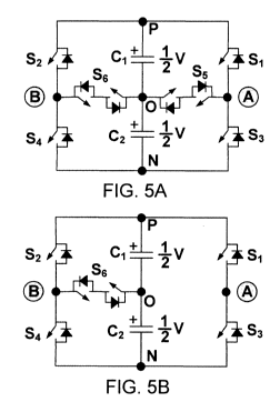
[0040] FIG. 5A shows a 5-level single phase inverter topology
with ac obtained between differential output nodes A and B .
The 5-level inverter comprises four unidirectional controlled
;.
switches
S,, Or S31 '54, two bidirectional controlled switches
s5 f S16 and two DC sources I T , I r in series. Typical.
2 2
unidirectional controlled switches comprise power
semiconductors such as Insu_ated-Gat,e Bipolar Transistors
(IG {T) with an anti --paral__..e:. diode across their
emitter-collector junctions. An ...G} '_[' is a three-terminal power
semiconductor device having an isolated Field Effect
Transistor (`'E_-') for the control input. (gate) and bipolar
power transistor as a switch (o:_ ~ector emitte_) e The power
semiconductor devices can also be M.eta7_ '~ c 1r
Transistors ansist~-.,r -s (MJrS:E'E,'_~', --s1, Integrated .- ' (rate-C~:_-
?rnm.utated.
Field-Effect
Thyristor_. (,=[GCT5), Gate Turn-Off Thyristors - (G""0s), or other
types. The 1G}5'_L' emitter is equivalent to a MO:SI-'.E source, or
an 1GCT' or G'TO anode. The IGET collector -is eru :.va lent to a
MOSFET drain or an IGCT or GTO cathode. this disclosure,
the unidirectional controlled switches are treated as two
terminal (collector-emitter) devices. For the
controlled switches S,, S2 F A r , 5I4 the anode of the
anti-parallel diode is coupled to the emitter. A bidirectional
controlled switch can be formed by coupling together the
CA 02789705 2012-08-13
WO 2011/100738 PCT/US2011/024864
emitters of two unidirectional controlled switches, The two DC
S urc(s - r -~' may be two discrete DC supplies or two
ca pacitors (c1,C,2) i which split one common DC supply (v) across
nodes P and N into two discrete su;~p1__..es in series. The
total number of unidirectional and bidirectional controlled
switches (s _x) is, the same as used in as prior art 5 Tel.
t-opology. The l eut-ral ground. -o~ ~e 0 can be positioned flexibly
c :..:
y
since 0Iuc is obtainer differentially and, not by clamping to a
neutrals
[0041] To avoid s Tor , circuiting the DC bus or the two DC
sources % , v' the follc:wina constraints are imposed on the
switch control scheme:
[0042] 8; and 83 can not be turned on simultaneously;
[0043] 5, and S. can not be turned on si.rultaneo. sly;
[0044] Y_, and S5 can not bf turned on simultaneously"
a
[00 ] 5_, and 54 car., not be ea on simultaneously;
[0046] X52 and S can not be turner, on simultaneously; and
[0047] 54 and S4 cannot be turned on simul~,:.rieous=yo
11
CA 02789705 2012-08-13
WO 2011/100738 PCT/US2011/024864
[0048] Under these switching constraints, a 5-level ac of t.put
waveform is synthesizes.from the differential voltage across
output node` A and B . For convenience, the .aerie.. source node
between the t.wo sources v , - -V is orounded. Outou-t nodes
2
and B can be switched using the unidirectional
controlled switches S,, S2, S, 1
controlled switches S,, S to connect to the po sir-ive P
common 0, and e,a-.-y% no~-. .s iPote-. ~ - -s)
[0049] FIG. 6A shows 4, table listing all combinations of
switch S states that--. generate a 5 _eve_ sinusoid (v
,
h
output nodes A and B . At any time, onl vT two switches a =e
e !~ A e G be closed I The
r 4? ~_ to e 1. _l.\ SJe to O'. t.4- a specific voltage level. redundant
switching choices can be alternated cycle by cycle
O balance the source 1/O.AtaGe sharing and istzatioln.
[0050] IG. 5l shows a. 5--level rove- ter topology using four
unidirectional (5 , S", S3 ,, ~!5) and one bidirectional ( , )
controlled Switches The required output voltage levels are
still ac sieved with the removal of one bidirectional
:c strolled switch S 5 from the full topology 5A) . FIG. 6F-?
shows a table listing all comr), nations of the switch S
states
[0051] During tie positive half-- cycle, node A _s clamped to
~= e
1] P (S __= l N 5 === (.. F) and lode c> ~~ switched amOi:lJ nodes
.~..: t ] , 3 is S
P,0,orrN ,;btai0V , + 1 V. and V respeec.tively. During the
ro -
negative half cycle, node A is clamped .=0 node N (Si= 0--'
5Si"= ON) and node B is switched. among nodes ,N',O,w-P to obtain
12
CA 02789705 2012-08-13
WO 2011/100738 PCT/US2011/024864
OP r - I V , and -V respective! y. El1G. 7 dhows the switch
2
conduct_ostates Sl f SZ f S, f Sc f S;; and resultant output ac
(V, for one cycle for the reduced topology 5-l.e.ve 1. inverter
tihc;wih in F- G. SF.
[0052] A MATLAB/ Simulink model of the embodiment was built to
simulate the basic operating pr' nciple. Under the lowest
~rea, .~eney sw j chin q scheme (Close to "he $undamer_tal
f r equeinc`y ,, 60 Hz) ..'1Gs. 8 and 9 clot the DC sources V P' r
2
configured as capacitors C. , C2 (with one common C supply (v)
rnSs nodes and N") their Vol-tag. different
r.c7 V. , under __
C.<
load conditions (top lots) and an observed Etc wave-for'm
;venerated (bot '.Jr( plots)
[0053] Two zero voltage , states are used alternatively to
balance the capacitor vc;ltaaet, `, V(,2. -FIG, 8 (upper plot)
shows that when capacitors C, and, Care la__~Je enough.
(1 2 , 000 pF r ' 00 ._)(} and the -ac load 1_c. not heavy (1.0 1 and
in in series) ,, the output (lower plot) 1'. L, aveforr t (s' 'ppe
fi
line) be odd---y,ymmet1.1_- and m rr_or_ -- ymn,et ?_ r ,:]: rt
e1.7_minate t C e component and a`1 eve o ~r harmonics , To
n cI~ _
cancel. certain to wer --orde:_ h.aI m o n csr .~le proper g e
each level of -the 7-1.eJe_l. inverter is chose-; to sat. _ .f1,
- cos 72O, + CfJg nO, 0
0054 ] -irfl
f,T v, 2
(1}
1
CA 02789705 2012-08-13
WO 2011/100738 PCT/US2011/024864
[0055] where 0, and 0, are the angles in radians for different
voltage levels (FIG. 7, V B versusU)t) and n is the harmonic order
be caicelled.
[0056] Al'--_ each inverter output level-, increasing switching
Pulses or using Pulse Width Modulation (PWM) techniques can
control the out=put voltage magnitude and fu tiler depress the
.,.M.II _ iI_d recluce output f .; ~ ter
lower-o-der harmonic spect- _
(inductor' and capacitor) size.
[0057] Embodiment are e sc:- 1.eabl.` and allow for the. number of
. .
inverter o tpu l~vel.s to l e increased by ads .nC S:J._ I a7_l. DC
sour_c :s and <]:~%. r_ r cells (-. :_d__re .1 nil. a.ci b~_d~rect.i~na7_
controlled switches)
[0058] _ I(J's . 1OA and _(_B= (lea t) show revel inverter's havinrl
(c-, sip
ful7_ tc_:' o1_og=-e with three ea =: DC y urr_.et
unidirectiorial con uro11ed switches S1 , 52 , S3 , S4 , S5 , S6 and
e _ rl t e l w a I~ s ,
i S, The a c
S S i S")
output may be o1 wined eit_^er across ~.hf-_', last inverter ci_'ll
(across cell node A and B , FIG. IOA) or the first inverter
cell (ac.--o :s cell nodes A and B, FIG. _C", B.f
[0059] For a 7-level inverter full top.logy, where are
r2 l ::lY1Ci c3 ,} t= L, : a j ~-_ C' ' +- C: a c i1 1 2, E' ~1 =: C ; e c. l
{1 G ~i' o -t t a ^ or
~.:~ ~.J_y~~F' 1 C' V C' l ,
exa_mp1e, t__er'e ,.ire four c__o_ces to ob:=...in zero vol,= ge, ,.hree
choices to Obtain a. V or V, two -ho"ces .for - or
3 i i
--' , a_^cl one choice fo- + ' or -V voltage level , By
3
sacrificing ,.he voltage stre s s of a single switch, the amount
of switches I'ay be reduced and genera..e the same oVj uu. FIGS.
14
CA 02789705 2012-08-13
WO 2011/100738 PCT/US2011/024864
10A and 10B (right) show a reduction in the total number of
unidirectional controlled switches from six to four and a
reduction in the number of bidirectional controlled switches
from four to two.
[0060] FIG. 11 shows a similar reduction for a 9--l.evel
inverter. FIG. 12 shows a table listing all combinations of
for both full the switch states 1_-1_ and reduced. inverter
topologie.s shown in FIG. 10B.
[0061] For higher level inverters, the switch reduced topology
is not unique. However, the minimum number of required
semiconductor switches is unique for desired in level
inverter. Embodiments provide a method to arrive at the number
of DC sources, and the number of unidirectional and
bidirectional controlled switches for a desired multilevel
inverter output.
[0062] FIG. 13 shows a table comparing different inverter
levels and their required number of switching devices. For
example, a l3-level inverter would require six split-rail DC
sources. For a full topology version, each DC source is
available. For a reduced topology version, the connections to
some DC sources are omitted. For a l3-level inverter, .he
maximum reduction of switching elements is twelve arriving at
minimum number of twenty.
[0063] FIG. 14 is a table comparing the number of electrical
components used in multilevel embodiment topologies with prior
art Wltilevel inverter topologies. FIG. 1.3 shows that full
topology embodiments are not desirable in terms of switch
number, while reduced topology embodiments offer a substantial
reduction A-I'i switches. ] For reduced l l switches. ~ Nltopologies, 'l
i'~leS, the reverse
CA 02789705 2012-08-13
WO 2011/100738 PCT/US2011/024864
blocking voltages of different semiconductor s can Ai I e
J switches
because some switches are across higher DC
voltages than other switches. Additionally, using less
split-rail DC sources, the voltage stress of switches is
higher compared co the same level conventional topology.
[0064] FIG. 15 shows a method for arriving at full and reduced
multilevel inverter topology embodiments. A d(-:s :.red number of
inverter . output levels in is selected, where in &5 is an
integer and an odd number (step 1501) . The number of DC
sources n in series is determined based on the output levels
in - I
in ,, where 3'E ___ . The DC sources n may be n equal discrete DC
supplies or n equal capacitors splitting a common DC supply
(step 1503).
[0065] The n DC sources are coupled together in series (where
the DC sources add together) and define a positive node P
the first DC source positive end, a negative node N at the
last 1DC. source negative end and one or more series source
nodes at each DC source series coupling beginning g with a fir_,st
series source node after the first source (steps 1505,
p _
1507) . if n capacitors are used, one common _ DC supply (V) is
coupled across the nodes P and _V
[0066] From the selected number of output levels in , a number
of r unidirectional controlled Cet-errmanen
switches ucs is l~n
depending on whether a full (steps 1509, 1513) or reduced.
(steps 1509, 1511) inverter topology is desired. FIG. 13 shows
the relationships of the full and reduced inverter topology
unidirectional controlled switch requirements. From .he total
number ucs of unidirectional control switches, inverter cells
are assembled.
16
CA 02789705 2012-08-13
WO 2011/100738 PCT/US2011/024864
[0067] An inverter cell comprises two unidirectional
controlled switches andd, two b __directional controlled switches.
An inve_'ter cell therefore requires si luniC irectior:a1
controller; switches . _ r'om the total number ucs of
Ues
unidirectional control switches, (cyuo'tient) c etermines the
6 number of inverter cells for the r: umber oI se' ected inver;.er
output leve ! s in . Ou = of the total number ucs of unidirectional
control wi,.ches, two ni ;=_e .,.~or.al control led, . wi'tches
remain (remainder) (step 15 5) As described above,, a
bird 'ectional controlled switch comprises two unidirectional
con-trolled switches coupled together, emitter'-to-emituer.
0068] For each ' ; -ertor cell, the two bili.r.. ecr
c t r, _iJna:1
controlled switches are coupled togee-he__ and common ve
forms a cell. series node. The other termina.l of each
bidirectional controlled switch -Ls coupled, l e d, to the el'.l__._,_er
terminal of one unidirection l_ cone-rolled switch, forming two
cell nodes (step 1-51'.7) . Each inverter_ cell therefore has one
cell se'_ _._es node and two cell nodes .
[0069] Eich inverter cell series node is coupled to a source
series node. The first source series node is coupled to the
cell series node .for a ce11. and the collector terminals o.f
_:.,. ed. switches,
that r_.e'.1_ - 's two un1.d1.. ect1_ona1_ c oc'n.,tr,:_?-1.switches,
switches, are '] c r ~ u p 7_ ed
T. the node P (.step 119) each remaining inverter cell.,
the cell series node for a cell is oupled to a followincr
s u: r_.` se:__..e cl ., and each ;;r.,:_d:_r_ _. i n:~l. controlled
switch's collector terminal _.oupled to a expect eve c:e1.7_
node o a pr" :_aus i.nverte:_ ce (step 7.521.)
1r
CA 02789705 2012-08-13
WO 2011/100738 PCT/US2011/024864
[0070] After all i_:verter cells have been coupled to
respective source series nodes and previous inverter cell's
cell nodes, two unidirectional controlled switches remain.
[0071] The emitter term:_nal for each of the two
unidirectional controlled y A
~. switches is coupled to the node
and each collector terminal is coupled to a respective cell
node of the inverter cell 3
o.h. ~,h .last 1.n;T~.e.,. -- ce.1_ (step 1523) The ac output may
be taken differentially across two series b1_c'1-- e' ona7_
controlled switches in one inverter cell (Step 1525)s or fro-n-,
fro-n-,
two cell nodes, where each cell node is in a different
inverter cell and the ac obtained differential-_y across two
bidirectional controlled _ switches where one o? more ~ s
_DC Sources
may interpose the two bidirectional - ep
controlled switches (step
[0072] Alternatively, rather than starting at the fi..st source
node, -~, series node -is s coupled
series the last source s. to a C.c_;7.l
series node for first cell and the emitter terminals of the
cell's two un.,:_dir_ectional controlled switches are coupled to
the node N . For each remaining inverter cell., the ce-11. series
node for a cell is coupled to a preceding source series node,
and each unidirectional controlled switch's emitter terminal
is coupled to a respective a prey,ious inverter
,e_.l lr.,.odt~ of
cell. The collector terminal for each of the two remaining
unidirectional ;a' controlled switches is coupled, e
to the node
any. ~.acl. emitter terminal .eretinal. .._..7.1. node
is coupled to a respective cell
of the last inverter Cell.
[0073] one or more in-level inverters may be cascaded together
to form a combined output having m"i . levels, FlG. 16 shows,
three or more 5-level inverters inverter 1, inverter 2, ..,
inverter x coupled together in a series cascade. The symbology
18
CA 02789705 2012-08-13
WO 2011/100738 PCT/US2011/024864
indicates inverter unidirectional controlled switches and.
bidirectional controlled switches used. in the topology. The
cascaded topology defines two output nodes A. and B across
the entire -r~ cascade. -a -
h Each individual il~;T~.rt.c_;r .-- ?-lwer_ter :]_,
inverter 2, ...,, inverter x used in a cascade has two
differential output nodes
xs x '
[0074] The output across two cascaded Level (ni:::5) inverters
produces a 9-level cascaded output (AC,BC) . If another 5-level
inverter were cascaded, a 13-level inverter output would
result. A cascade may be continued until a desired number
output levels are reached depending on the levels of the
inverters used in the cascade. For exam.ple, a cascade of x
5---.le- e.l inverters outputs (4.x+1) levels
[0075] FIG, 17 shows plots for two ----eve'_ inverters inverter
1 A.,B_ , inverter 2 A2,B`z and a plot of their cascaded output
.1, Bt" over one cycle OW). i 9'-.leve.l (YAhx = 2; 4x+1 =ti) output is
c,
obtained. The individual DC sources V in inverter! and
inverter 2 add depending when their DC sources are switched
(a;=u2,aca.,..) during the cycle. All of the DC sources used in
one inverter are equal and each inverter's DC sources are
isolated 'lat2Cl = from another tnveArter .. '_ DL, sources. e a c
However, each
individual inverter in a cascade may ~ rime DC source voltages
that are different from another inverter in the cascade, anC
inverter levels can be different from one another .
[0076] The cascade topology reduces the voltage and current
limitations ~r semiconductors of ~.hpower use d, and with
increasing inverter levels, the output approaches 'approaches a pure
19
CA 02789705 2012-08-13
WO 2011/100738 PCT/US2011/024864
. ~
sinusoidal ac waveform exhibiting low distortion without
requiring passive filtering components.
[0077] Embodiments are single phase mu_._t.._ level. inverter
topologies using a .full--bridge approach with bidirectional
interconnections. Compared to prior art diode--clamped or
flying--capacitor multilevel topologies, the required
split-rail DC sources are less, and the number of required
power switches can be reduced by removing redundant switching
states. Using asymmetrical DC sources, the output levels can
be significantly increased. Embodiments can he applied to
solar photovoltaic, (micro-inverters) and energy storage
(multiple battery cel-ls) apr ica; ions.
[0078] One or more embodiments the present invention have
been described. Nevertheless, it will be understood that
various modifications may be made without departing from the
spirit and scope of the invention. According-11.y, other
embodiments .are within the scope of the ~ f~ ,1.1_o,ti'_..n. q -,-aim.s
,.