Note: Descriptions are shown in the official language in which they were submitted.
CA 02790077 2012-08-15
DESCRIPTION
TITLE OF INVENTION
Semiconductor Device and Method of Manufacturing the Same
TECHNICAL FIELD
The present invention relates to a semiconductor device and a method of
manufacturing the same, and more particularly to a semiconductor device having
a
silicon carbide substrate and a method of manufacturing the same.
BACKGROUND ART
For a method of manufacturing a semiconductor device including a silicon
carbide substrate, a technique for forming an ohmic electrode on the silicon
carbide
substrate has been developed.
For example, according to Japanese Patent Laying-Open No. 7-99169 (PTL 1),
by forming an Ni-Si alloy layer or a stack of Si and Ni on an SiC base (a
silicon carbide
substrate), NiSi2 (33 atomic % of Ni and 67 atomic % of Si) can be formed
without
supply of Si from the SiC base and an electrode in ohmic contact with the SiC
base is
obtained. In addition, according to this publication, when Ni is not more than
33% in
an atomic ratio, Si is excessive and conductivity is impaired, and when Ni is
not less
than 67%, excessive Ni is present at an interface between NiSi2 and SiC and
the
interface becomes discontinuous. Further, according to this publication, since
Si is
not supplied from SiC, such a phenomenon that excessive C diffuses into Ni and
it is
precipitated as graphite at a surface of an electrode does not occur.
CITATION LIST
PATENT LITERATURE
PTL 1: Japanese Patent Laying-Open No. 7-99169
SUMMARY OF INVENTION -
TECHNICAL PROBLEM
As described above, in forming an electrode (electrode layer) having Ni atoms
and Si atoms, in order to enhance electrical conductivity of the electrode
layer, a ratio
-1-
CA 02790077 2012-08-15
of Ni should be increased. When the ratio of Ni is increased, many C atoms are
precipitated from the silicon carbide substrate to the surface of the
electrode layer
during annealing for forming the electrode layer. Therefore, it has been
difficult to
achieve both of enhancement in electrical conductivity of the electrode layer
and
suppression of precipitation of C atoms at the surface of the electrode layer.
Therefore, an object of the present invention is to provide a semiconductor
device capable of achieving both of improvement in electrical conductivity of
an
electrode layer and suppression of precipitation of C atoms at a surface of
the electrode
layer and a method of manufacturing the same.
SOLUTION TO PROBLEM
A semiconductor device according to the present invention has a silicon
carbide
substrate and an electrode layer. The electrode layer lies on the silicon
carbide
substrate in contact therewith and has Ni atoms and Si atoms. The number of Ni
atoms is not less than 67% of the total number of Ni atoms and Si atoms. A
side of
the electrode layer at least in contact with the silicon carbide substrate
contains a
compound of Si and Ni. On a surface side of the electrode layer, C atom
concentration is lower than Ni atom concentration.
According to this semiconductor device, in the electrode layer, the number of
Ni atoms is not less than 67% of the total number of Ni atoms and Si atoms.
Thus, as
compared with a case where this percentage is lower than 67%, electrical
conductivity
of the electrode layer can be enhanced. In addition, according to this
semiconductor
device, on the surface side of the electrode layer, C atom concentration is
lower than Ni
atom concentration. Thus, when a metal pad layer in contact with the surface
side of
the electrode layer is formed, this metal pad layer is less likely to peel
off.
Preferably, on the surface side of the electrode layer, C atom concentration
is
lower than 3%.
Preferably, the semiconductor device has a metal pad layer in contact with the
surface side of the electrode layer. The metal pad layer is preferably an Al
layer.
Preferably, the metal pad layer includes an adhesive layer formed on the
electrode layer
-2-
CA 02790077 2012-08-15
and a main body layer formed on the adhesive layer. The adhesive layer is
composed
of any of Ti, TiW, and TiN.
Preferably, Si atom concentration on the surface side of the electrode layer
is
lower than 30%. Thus, electrical conductivity of the electrode layer can
further be
enhanced.
A method of manufacturing a semiconductor device according to the present
invention has the following steps. A silicon carbide substrate is prepared. A
material layer lying on the silicon carbide substrate in contact therewith and
having Ni
atoms and Si atoms is formed. The number of Ni atoms is not less than 67% of
the
total number of Ni atoms and Si atoms. By annealing the material layer with
laser
beams, an electrode layer of which side at least in contact with the silicon
carbide
substrate contains a compound of Si and Ni is formed.
According to this method of manufacturing a semiconductor device, in the
material layer serving as a material for the electrode layer, the number of Ni
atoms is
not less than 67% of the total number of Ni atoms and Si atoms. Thus, as
compared
with a case where this percentage is lower than 67%, electrical conductivity
of the
electrode layer can be enhanced. In addition, according to this method of
manufacturing a semiconductor device, annealing is carried out in a short
period of
time by using laser beams. Thus, as compared with a case where annealing is
carried
out for a longer period of time, diffusion of C atoms can be suppressed.
Therefore, C
atom concentration on the surface side of the electrode layer can be lowered.
Thus,
when a metal pad layer in contact with the surface side of the electrode layer
is formed,
this metal pad layer is less likely to peel off.
Preferably, a metal pad layer is formed on the electrode layer. The metal pad
layer preferably includes an Al layer. Preferably, the step of forming a metal
pad
layer includes the steps of forming an adhesive layer on the electrode layer
and forming
a main body layer on the adhesive layer. The adhesive layer is composed of any
of Ti,
TiW, and TiN.
The step of forming a material layer may include the step of forming a mixed
-3-
CA 02790077 2012-08-15
layer of Si and Ni. Alternatively, the step of forming a material layer may
include the
step of stacking an Si layer and an Ni layer.
ADVANTAGEOUS EFFECTS OF INVENTION
As described above, according to the present invention, enhancement in
electrical conductivity of the electrode layer and suppression of
precipitation of C
atoms at the surface of the electrode layer can both be achieved.
BRIEF DESCRIPTION OF DRAWINGS
Fig. 1 is a cross-sectional view schematically showing a construction of a
semiconductor device in a first embodiment of the present invention.
Fig. 2 is a cross-sectional view schematically showing a first step (A) and a
second step (B) in a method of manufacturing the semiconductor device in Fig.
1.
Fig. 3 is a cross-sectional view schematically showing a variation of the
semiconductor device in Fig. 1.
Fig. 4 is a cross-sectional view schematically showing one step in a method of
manufacturing a semiconductor device in a second embodiment of the present
invention.
Fig. 5 is a cross-sectional view schematically showing a construction of a
semiconductor device in a third embodiment of the present invention.
Fig. 6 shows an atomic concentration profile of a semiconductor device in a
first comparative example.
Fig. 7 shows an atomic concentration profile of a semiconductor device in a
second comparative example.
Fig. 8 shows an atomic concentration profile of a semiconductor device in a
third comparative example.
DESCRIPTION OF EMBODIMENTS
An embodiment of the present invention will be described hereinafter with
reference to the drawings.
(First Embodiment)
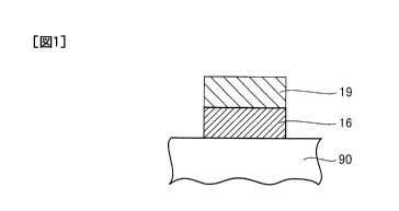
Referring to Fig. 1, a semiconductor device in the present embodiment has a
-4-
CA 02790077 2012-08-15
silicon carbide substrate 90, an electrode layer 16, and a metal pad layer 19.
Electrode layer 16 lies on silicon carbide substrate 90 in contact therewith
and
has Ni atoms and Si atoms. The number of Ni atoms is not less than 67% of the
total
number of Ni atoms and Si atoms. More specifically, general composition of a
material for electrode layer 16 is a mixture of Ni not lower than 67 atomic %
and Si
which is a substantial remainder. It is noted that an additive other than Ni
and Si may
be added to a material for electrode layer 16 as necessary. In addition, a
material for
electrode layer 16 may contain an inevitable impurity in an industrial
manufacturing
method.
Preferably, the number of Si atoms in electrode layer 16 is not less than 10%
of
the total number of Ni atoms and Si atoms.
A side of electrode layer 16 at least in contact with silicon carbide
substrate 90
contains a compound of Si and Ni, that is, nickel silicide. Thus, electrode
layer 16
and silicon carbide substrate 90 establish ohmic contact with each other.
Namely,
electrode layer 16 has a function as an ohmic electrode.
On a side of electrode layer 16 in contact with silicon carbide substrate 90
(a
lower side in the drawing), the compound above is generally Ni2Si. Namely, on
the
side of electrode layer 16 in contact with silicon carbide substrate 90, a
ratio of the
number of Ni atoms to the total number of atoms of Ni and Si is approximately
2/3, that
is, approximately 67%. This ratio is higher on the surface side (an upper side
in the
drawing) of electrode layer 16, and in an extreme case, it may be a value
close to 100%.
Namely, aside from an inevitable impurity in an industrial manufacturing
method or
inevitable deposits from an external environment, the surface side of
electrode layer 16
may substantially be composed of Ni. In this case, electrical conductivity on
the
surface side of electrode layer 16 is higher than in a case where Si is
significantly
contained.
On the surface side of electrode layer 16, C atom concentration is lower than
Ni
atom concentration. Preferably, this C atom concentration is lower than 3% and
more
preferably lower than 1 %. More preferably, substantially no C atom is present
on the
-5-
CA 02790077 2012-08-15
surface side of electrode layer 16. Namely, aside from deposition of
inevitable C
atoms from an external environment, the surface side of electrode layer 16 may
substantially be composed of Ni.
Here, atomic concentration on the surface side refers to a ratio of the number
of
specific atoms to the total number of atoms in a region extending from a
surface (an
upper surface in the drawing) of electrode layer 16 to a depth of 5 nm. This
atomic
concentration can be measured with element analysis high in resolution in a
direction of
depth, and it can be measured, for example, with SIMS (Secondary Ion Mass
Spectroscopy). If a surface of electrode layer 16 is exposed to atmosphere in
an
operation for preparation for measurement, the surface of electrode layer 16
should be
cleaned. Cleaning is, for example, ultrasonic cleaning using such an organic
solvent
as acetone.
Preferably, the surface of electrode layer 16 itself is a surface from which
no
substance has been removed by etching, polishing, or the like. Thus, the step
of
forming electrode layer 16 is further simplified. Even in this case, however,
a
contaminant that has deposited onto the surface of electrode layer 16 from an
external
environment after electrode layer 16 is formed may be removed. Removal can be
achieved, for example, by cleaning as described above.
Metal pad layer 19 is in contact with the surface side of electrode layer 16.
Preferably, metal pad layer 19 is either an Al layer or an Al-Si layer.
A method of manufacturing a semiconductor device in the present embodiment
will now be described.
Referring to Fig. 2(A), silicon carbide substrate 90 is initially prepared.
Then,
a material layer 50a lying on silicon carbide substrate 90 in contact
therewith and
having Ni atoms and Si atoms is formed. The number of Ni atoms is not less
than
67% of the total number of Ni atoms and Si atoms. Material layer 50a is a
mixed
layer of Si and Ni. This mixed layer can be formed, for example, by
simultaneously
sputtering a target composed of Si and a target composed of Ni.
Preferably, the number of Si atoms in material layer 50a is not less than 10%
of
-6-
CA 02790077 2012-08-15
the total number of Ni atoms and Si atoms.
Referring further to Fig. 2(B), as annealing treatment, silicon carbide
substrate
90 on which material layer 50a (Fig. 2(A)) has been formed is irradiated with
laser
beams. As a result of this annealing, electrode layer 16 (Fig. 2(B)) is formed
from
material layer 50a. This annealing is carried out such that a side of
electrode layer 16
at least in contact with silicon carbide substrate 90 contains a compound of
Si and Ni,
that is, nickel silicide.
Preferably, the laser beams have a wavelength not longer than 386 nm, which is
a wavelength corresponding to a band gap of silicon carbide. Thus, laser beams
are
absorbed in the surface of silicon carbide substrate 90. Light beams having a
wavelength of 355 nm, which are third harmonics of YAG laser or YVO4 laser,
can be
employed as such laser beams.
Output density of laser beams is not less than 0.5 J/cm2 and not more than 1.5
J/cm2 and more preferably not less than 0.7 J/cm2 and not more than 1.3 J/cm2.
Thus,
a sufficient annealing function can be obtained and damage due to laser beams
can be
suppressed.
Laser beams have a pulse width not less than 10 ns and not more than 10 .is
and
more preferably not less than 50 ns and not more than 1 s. Thus, annealing
can be
carried out in a sufficiently short period of time while laser having a
practical pulse
width is being used.
Referring again to Fig. 1, metal pad layer 19 is formed on electrode layer 16.
Metal pad layer 19 is preferably an Al layer. The semiconductor device in the
present
embodiment is obtained as above.
According to the semiconductor device in the present embodiment, in electrode
layer 16, the number of Ni atoms is not less than 67% of the total number of
Ni atoms
and Si atoms. Thus, as compared with a case where this percentage is lower
than 67%,
electrical conductivity of electrode layer 16 can be enhanced. In addition,
according
to this semiconductor device, the surface side of electrode layer 16 has C
atom
concentration lower than the sum of Si atom concentration and Ni atom
concentration.
-7-
CA 02790077 2012-08-15
Thus, when metal pad layer 19 in contact with the surface side of electrode
layer 16 is
formed, this metal pad layer 19 is less likely to peel off.
Preferably, Si atom concentration on the surface side of electrode layer 16 is
lower than 30%. Thus, electrical conductivity of electrode layer 16 can
further be
enhanced.
In addition, according to the method of manufacturing a semiconductor device
in the present embodiment, in material layer 50a serving as a material for
electrode
layer 16, the number of Ni atoms is not less than 67% of the total number of
Ni atoms
and Si atoms. Thus, as compared with a case where this percentage is lower
than 67%,
electrical conductivity of electrode layer 16 can be enhanced.
Further, by using laser beams, annealing is carried out in a short period of
time.
Thus, as compared with a case where annealing for a longer period of time,
such as
lamp annealing, is carried out, diffusion of C atoms can be suppressed.
Therefore, C
atom concentration on the surface side of electrode layer 16 can be lowered.
Thus,
when metal pad layer 19 in contact with the surface side of electrode layer 16
is formed,
metal pad layer 19 is less likely to peel off.
Preferably, the number of Ni atoms in electrode layer 16 or material layer 50a
is
not less than 70% of the total number of Ni atoms and Si atoms. Thus, the
function
and effect described above can more reliably be obtained. Further preferably,
the
number of Ni atoms is not more than 90% of the total number of Ni atoms and Si
atoms.
Thus, diffusion of C atoms from silicon carbide substrate 90 can further be
suppressed.
A variation of the present embodiment will now be described.
Referring to Fig. 3, a metal pad layer 19V in a semiconductor device according
to the present variation includes an adhesive layer 19a formed on electrode
layer 16 and
a main body layer 19b formed on adhesive layer 19a. Adhesive layer 19a is
composed of any of Ti, TiW, and TiN. Main body layer 19b is preferably an Al
layer
or an Al-Si layer.
According to the present variation, adhesion of metal pad layer 19V to
electrode
layer 16 can further be enhanced.
-8-
CA 02790077 2012-08-15
(Second Embodiment)
Referring mainly to Fig. 4, in the present embodiment, a material layer 50b is
formed instead of material layer 50a (Fig. 2(A)). The step of forming material
layer
50b includes the step of stacking an Si layer 51 and an Ni layer 52.
Preferably, an
uppermost layer of the formed stack is Ni layer 52. Thus, since a ratio of Ni
atoms on
the surface side of electrode layer 16 obtained after annealing can be
increased,
electrical conductivity on the surface side of electrode layer 16 can be
enhanced.
Since features other than the above are substantially the same as those in the
first embodiment described above, the same or corresponding elements have the
same
reference characters allotted and description thereof will not be repeated.
According to the present embodiment, it is not necessary to form a mixed layer
of Ni and Si as in the first embodiment.
(Third Embodiment)
In the present embodiment, one example of a further detailed structure of the
semiconductor device in the first or second embodiment described above will be
described.
Referring to Fig. 5, a semiconductor device in the present embodiment is a
vertical MOSFET (Metal Oxide Semiconductor Field Effect Transistor), and it
has
silicon carbide substrate 90, electrode layer 16, metal pad layer 19, a gate
insulating
film 15, and a gate electrode 17. Silicon carbide substrate 90 has an n+ layer
11, an n
layer 12, a p body layer 13, an n+ source region 14, and a p+ region 18.
Electrode layer 16 is provided so as to be in ohmic contact with each of n+
source region 14 and p+ region 18 at one surface (an upper surface in the
drawing) of
silicon carbide substrate 90. Electrode layer 16 has a thickness, for example,
approximately from 100 to 200 nm.
Gate electrode 17 is provided on one surface (the upper surface in the
drawing)
of silicon carbide substrate 90 with gate insulating film 15 being interposed,
and it is
opposed to a channel region 13A which is a surface side of p body layer 13. In
addition, on the other surface (a lower surface in the drawing) of silicon
carbide
-9-
CA 02790077 2012-08-15
substrate 90, a drain electrode 20 is provided.
According to the present embodiment, a vertical MOSFET having electrode
layer 16 high in electrical conductivity and metal pad layer 19 less likely to
peel off is
obtained.
It is noted that a vertical IGBT (Insulated Gate Bipolar Transistor) may be
constructed instead of a vertical MOSFET by forming a p collector layer on a
side of
silicon carbide substrate 90 facing drain electrode 20. Alternatively, a
structure in
which a gate electrode is embedded in a trench formed in a silicon carbide
substrate
with a gate insulating film being interposed (a trench gate structure) may be
employed.
(Comparative Example)
A comparative example of the present invention will be described with
reference to data of a concentration profile using SIMS. Since a metal pad
layer was
not formed on a surface of a metal layer, a portion in the vicinity of a
sputtering time
period of 0 in a concentration profile corresponds to a surface of an
electrode layer. In
addition, a sputtering rate was set to approximately 10 nm/minute. Further,
before
measurement, surface cleaning treatment was performed. A comparative example
will
specifically be described below.
(First Comparative Example)
An Ni layer was employed instead of material layer 50a. In addition, lamp
annealing was employed instead of laser annealing.
Referring to Fig. 6, at a surface of an electrode layer (in the vicinity of 0
on the
abscissa of the graph), C atoms occupied half or more of atoms. In addition,
across
the entire electrode layer, each of C atoms and Si atoms was present at a
significant
ratio. Further, Ni atoms diffused toward a deeper portion, that is, toward the
inside of
the silicon carbide substrate.
(Second Comparative Example)
Such a stack as having Ni of 80 atomic % and Si of 20 atomic % was employed
as material layer 50b (Fig. 4). In addition, lamp annealing was employed
instead of
laser annealing.
-10-
CA 02790077 2012-08-15
Referring to Fig. 7, as in the first comparative example, at the surface of
the
electrode layer (in the vicinity of 0 on the abscissa of the graph), C atoms
occupied half
or more of atoms.
(Third Comparative Example)
A layer lower in Ni ratio was employed instead of material layer 50a (Fig.
2(A)).
Specifically, a mixed layer having composition of Ni of 65 atomic % and Si of
35
atomic % was employed. In addition, lamp annealing was employed instead of
laser
annealing. Average electrical conductivity of the obtained electrode layer was
lower
than in the example of the present invention.
Referring to Fig. 8, across the entire electrode layer, Si atoms were present
at a
significant ratio. Namely, in the electrode layer, there was no portion
composed
substantially of Ni.
It should be understood that the embodiments disclosed herein are illustrative
and non-restrictive in every respect. The scope of the present invention is
defined by
the terms of the claims, rather than the description above, and is intended to
include any
modifications within the scope and meaning equivalent to the terms of the
claims.
REFERENCE SIGNS LIST
16 electrode layer; 19 metal pad layer; 50a, 50b material layer; 51 Si layer;
52
Ni layer; and 90 silicon carbide substrate.
-11-