Note: Descriptions are shown in the official language in which they were submitted.
CA 02790395 2012-08-17
WO 2011/103508 PCT/US2011/025548
SMARTCARD INTERCONNECT
[0001] This application claims the benefit of U.S. Provisional Application No.
61/306,431,
filed February 19, 2010, entitled "Smart Card Interconnect," which is hereby
expressly
incorporated by reference in its entirety for all purposes.
BACKGROUND
[0002] Coil antennas are commonly used in contactless smart cards. Contactless
smart card
antennas can be manufactured with etched or printed antennas. Smart card
antennas can also be
formed using round wire using ultrasonics or thermal compression to embed the
wire into a
plastic substrate. Regardless of how the antennas are formed, the antennas
need to be created
high precision and/or be tuned to a specific inductance. The coil antenna is
then attached to and
integrated circuit (IC) module, e.g., via terminal areas on the IC module.
Attaching the wire
ends to a delicate IC module has proven to be a difficult task because the IC
module can be
damaged while the antenna coil is being attached to the terminal areas of the
IC module.
Different sized IC modules can also require redesign of the entire coil
antenna due to the length
of the antenna wire changing in order to be attached to a larger or smaller IC
module.
SUMMARY
[0003] The ensuing description provides preferred exemplary embodiment(s)
only, and is not
intended to limit the scope, applicability or configuration of the disclosure.
Rather, the ensuing
description of the preferred exemplary embodiment(s) will provide those
skilled in the art with
an enabling description for implementing a preferred exemplary embodiment. It
being
understood that various changes may be made in the function and arrangement of
elements
without departing from the spirit and scope as set forth in the appended
claims.
[0004] In one embodiment, an inlay for a smartcard, includes a substrate, a
first trace attached
to the substrate a second trace attached to the substrate and an antenna with
a first end and a
second end. The first end of the antenna is coupled to a first area of the
first trace, and the
second end of the antenna is coupled to a first area of the second trace. A
second area of the first
trace and a second area of the second trace are configured to be coupled to an
integrated circuit
1
CA 02790395 2012-08-17
WO 2011/103508 PCT/US2011/025548
(IC) or IC module, and the first area of the first trace is located away from
the second area of the
first trace and the first area of the second trace is located away from the
second area of the
second trace.
[0005] In another embodiment, a method for assembling an inlay of a smartcard
includes
attaching a first trace to a substrate, attaching a second trace to the
substrate, attaching an
antenna wire to the substrate, coupling a first end of the antenna wire to a
first area of the first
trace, and coupling a second end of the antenna wire to a first area of the
second trace. A second
area of the first trace and a second area of the second trace are configured
to be coupled to an
integrated circuit (IC) or IC module, and the first area of the first trace is
located away from the
second area of the first trace and the first area of the second trace is
located away from the
second area of the second trace.
[0006] Items and/or techniques described herein may provide one or more of the
following
capabilities. Traces can be attached to a carrier strip to make pre-formed
singulated carriers, and
then attached to smart card inlays during down time of an assembly line for
manufacturing
smartcards. A sheet of smart card inlays (e.g., a sheet of 80 or 100 cards)
with antennas already
formed and connected to the traces can be made in advance and then an IC
module can be
attached to the traces. Thus, the more delicate work of forming the antennas
is already
completed before the IC modules are attached. The traces can be sized to fit
multiple IC
modules and therefore provide flexibility in which IC modules are used with
the smart card
inlays.
BRIEF DESCRIPTION OF THE DRAWINGS
[0007] FIG. IA depicts a example of a smartcard inlay in accordance with the
disclosure.
[0008] FIG. IB depicts another example of a smartcard inlay in accordance with
the
disclosure.
[0009] FIG. 2 depicts an example of a sheet of smartcard inlays in accordance
with the
disclosure.
[0010] FIGS. 3A, 3B, 3C and 3D depict examples of cross-sectional views of
finished
smartcards including smartcard inlays in accordance with the disclosure.
2
CA 02790395 2012-08-17
WO 2011/103508 PCT/US2011/025548
[0011] FIGS. 4A and 4B depict examples of rolls or coils of singulated
carriers that could be
utilized in forming smartcard inlays in accordance with the disclosure.
[0012] FIG. 5 is a flow diagram of an embodiment of a process for forming
smartcards
including smartcard inlays in accordance with the disclosure.
[0013] FIG. 6 is a flow diagram of another embodiment of a process for forming
smartcards
including smartcard inlays in accordance with the disclosure.
[0014] FIG. 7 is a flow diagram of yet another embodiment of a process for
forming
smartcards including smartcard inlays in accordance with the disclosure.
[0015] The features, objects, and advantages of embodiments of the disclosure
will become
more apparent from the detailed description set forth below when taken in
conjunction with the
drawings. In the drawings, like elements bear like reference labels. Various
components of the
same type may be distinguished by following the reference label with a dash
and a second label
that distinguishes among the similar components. If only the first reference
label is used in the
specification, the description is applicable to any one of the similar
components having the same
first reference label irrespective of the second reference label.
DESCRIPTION
[0016] The ensuing description provides preferred exemplary embodiment(s)
only, and is not
intended to limit the scope, applicability or configuration of the disclosure.
Rather, the ensuing
description of the preferred exemplary embodiment(s) will provide those
skilled in the art with
an enabling description for implementing a preferred exemplary embodiment. It
is understood
that various changes may be made in the function and arrangement of elements
without departing
from the spirit and scope as set forth in the appended claims.
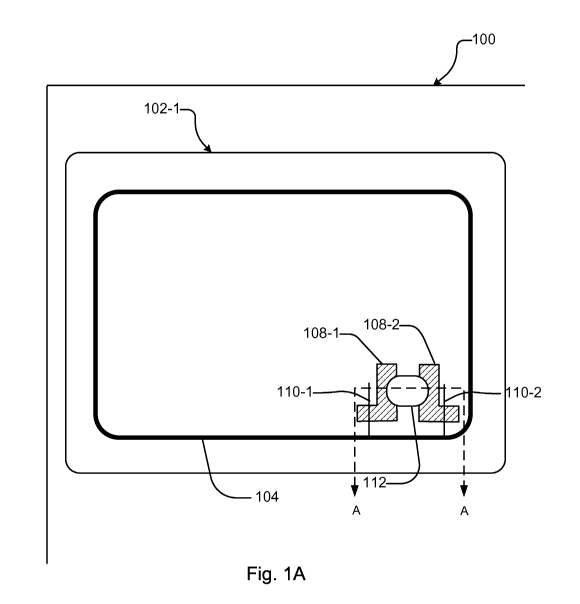
[0017] Referring initially to FIG. IA, an embodiment of a smartcard inlay 102-
1 formed on a
substrate sheet 100 is shown. This embodiment has a wire antenna 104 that
could be embedded
into the sheet 100 or mandrel wound in various embodiments. The substrate 100
can be made of
a plastic such as PET or PVC or paper. There is a first trace 108-1 and a
second trace 108-2 on
the substrate 100. These traces 108 can be etched, printed or silkscreened
onto the substrate 100.
The traces 108 can be adjacent to a cutout formed in the substrate 100 that at
least partially
3
CA 02790395 2012-08-17
WO 2011/103508 PCT/US2011/025548
accepts an integrated circuit (IC) or IC module 112. The cutout can also be
formed in an upper
or lower layer, not shown, that covers the substrate 100 and the cutout at
least partially accepts
the IC module 112. The cutout can be omitted entirely if a layer covering the
substrate 100 and
the IC module 112 is formed by controlled lamination that causes the upper
layer material to
flow over the IC module 112, resulting in a flat card surface. The term IC
module is used herein,
but in each instance a bare IC, multi-chip module or other assembly could also
be used.
[0018] Antenna wire leads 110-1 and 110-2 extend from ends of the wire antenna
104 and
extend over the areas where the traces 108-1 and 108-2, respectively, are
located. The traces 108
could have solder bumps for mounting the antenna 104 and/or the IC module 112
through a
heating process or soldering process. The wire leads 110 can be embedded into
the substrate 100
in areas outside of the traces 108 and not embedded, e.g., allowed to lie on
the substrate 100, in
the areas where the traces 108 are located. This will prevent damage of the
traces 108 during the
antenna embedding process, if the traces are already formed on the substrate
100.
[0019] The IC module 112 in this example partially overlays the traces 108
outside of the
cutout, if any cutout is present. Where there is overlap, the IC module 112
can be electrically
connected to the traces 108, e.g., by soldering a lead frame of the IC module
112 to the traces
108, to indirectly couple any attached antenna 104 to the IC module 112. The
IC module 112
can be connected to the traces 108 before or after the antenna 104 is attached
to the substrate 100
and/or the traces 108. In this embodiment, the IC module 112 is not directly
connected to the
antenna 104.
[0020] The antenna 104 could be mandrel wound or embedded into the substrate
100. The
antenna 104 is connected to the traces 108 via the wire leads 110 and neither
wire lead 110-1 or
110-2 is connected directly to the IC module 112. A mandrel wound antenna 104
could be
embedded into the substrate 100 all at once before or after connection with
the traces 108. The
antenna 104 has the one end connected to the first trace 108-1, wound while
embedding into the
substrate 100 next, and the other end connected to the second trace 108-2
last; or any
permutation of the sequence of these three steps could be done in various
embodiments.
[0021] When a cutout is formed in the substrate 100, this could be done before
or after the
traces 108 are applied to the substrate 100. The traces 108 could have other
shapes around the
cutout, but in any event, they are electrically isolated from each other. The
cutouts could be
4
CA 02790395 2012-08-17
WO 2011/103508 PCT/US2011/025548
done to a whole sheet having a number of inlays. Similarly, the traces 108
could be applied to a
whole sheet at once. Other traces 108 could be applied to the substrate for
other antennas or
other IC modules in various embodiments.
[0022] The dimensions of the traces 108 depends on the size of the IC module
112 and the
width of the antenna wire leads 110. Typically, lead frame flanges of the IC
module 112 are
about 2 mm where the lead frame attaches to the traces 108. The diameter of
the wire is about
.004 inches (4 mils) or. I mm.. The lower portion of the traces 108, where the
wire leads 110
attach, is typically about 2 to 10 times as wide as the antenna wire 104, or
about 2 mm to about
mm. The upper portion of the traces 108, where the IC module 112 attaches, is
typically at
10 least as wide as the lead frame flanges or about 1 mm to about 4 mm. The
size of the traces 108
will affect the inductance of the whole antenna, including the antenna wire
104, the wire leads
110 and the traces 108, but the length of the antenna wire can be adjusted to
compensate for the
inductance of the traces 108.
[0023] With reference to FIG. 1B, another embodiment of the smartcard inlay
102-2 is shown.
This embodiment has the traces 108 formed on a singulated carrier 116. The
singulated carrier
116 could be plastic, circuit board, kapton or other tape. The singulated
carrier 116 could be
configured to allow pick and place machines for automated assembly. The
singulated carrier 116
could be glued, heat welded or have an adhesive backing to allow placement on
the substrate
100. The singulated carrier 116 could have solder bumps for the antenna 104
and/or the IC
module 112.
[0024] Some embodiments place the singulated carrier 116 on the substrate 104
first before
connecting the IC module 112, while others connect the singulated carrier 116
to the IC module
112 before that assembly is connected to the substrate 100. One embodiment
connects a mandrel
wound antenna 104 to the singulated carrier 116 prior to that assembly being
attached to the
substrate 100. The singulated carrier 116 could be placed on the substrate 100
before a cutout is
made, if a cutout is present, in both the singulated carrier 116 and the
substrate 104. Other
embodiments have a cutout in the singulated carrier 116 that is matched to a
cutout in the
substrate 104 or where the cutout will later be formed in the substrate 104.
Other embodiments
have no cutout.
5
CA 02790395 2012-08-17
WO 2011/103508 PCT/US2011/025548
[0025] The singulated carrier 116 could be formed in a sheet to match a sheet
of substrates so
that multiple singulated carriers 116 can be mated with the sheet of substrate
at once. There
could be alignment markings on the singulated carrier 116 or sheet of the
singulated carriers 116
to ease alignment. Some embodiments use cutouts in the substrate 100 or sheet
of substrate 100
for alignment with the singulated carrier 116 or sheet of singulated carriers
116.
[0026] Referring next to FIG. 2, a sheet 200 of smartcard inlays 102 is shown.
Any number of
smartcard inlays 102 could be formed in the sheet 200. The antennas 104 could
be embedded or
placed sequentially in the sheet 200. The traces 108) could be formed on a
mating sheet or
applied to the sheet 200. The sheet 200 could be formed with cutouts, antennas
104 and traces
108 before any IC modules 112 are attached. The antennas 104 could be attached
to the traces
108 for all inlays prior to attachment of any IC module 112.
[0027] FIGS. 3A, 3B, 3C and 3D depict various cross-sectional views, at the
plane cut line A-
A of FIG. IA, of finished smartcards including the smartcard inlays of FIGS.
IA and 113.
Referring to FIG. 3A, a first cross section 300-1 includes two layers. The
traces 108-1 and 108-
2 are formed on a substrate layer 315, where the substrate 315 is equivalent
to the substrate 100
of FIGS. IA and 113. The traces 108 can be etched, printed or silk-screened
onto the substrate
315 or the traces 108 can be formed on the singulated carrier 116 (not shown
in FIG. 3A) that is
attached to the substrate 100. The wire leads 110-1 and 110-2 are shown
embedded into the
substrate 315. As discussed above, the wire leads 110 could be attached via
adhesive to lie
above the substrate 315, As illustrated, the cross section 300-1 does not show
the portion of the
traces 108 where the wire leads 110 are attached. At the attachment portions,
the wire leads
could be above or below the traces 108, but not embedded, at least not
entirely in the substrate,
in order to provide electrical contact.
[0028] The IC module 112-1 includes an IC chip 3 10-1 and a lead frame 312-1.
The IC chip
310-1 can include an integrated circuit (IC) encased within an encasement
(e.g., made of epoxy).
As an alternative to an encased IC coupled to a lead frame 312, some IC
modules 112 could be
simply an IC attached to a carrier including two isolated conductive portions
electrically coupled
to ball bonds of the IC. Isolated ends of the lead frame 312-1 are
electrically coupled to the
traces 108-1 and 108-2, respectively. The traces 108-1 and 108-2 electrically
couple the lead
wires 110-1 and 110-2 indirectly to respective ends of the lead frame 312-1.
6
CA 02790395 2012-08-17
WO 2011/103508 PCT/US2011/025548
[0029] An upper finishing layer 320 covers the IC module 112-1, the traces 108
and the
substrate 315. In this case, there is no cutout portion in either the
substrate 315 or the upper
layer 320. The upper layer 320 can be a laminate that is formed in a
controlled lamination cycle
that causes the laminate to flow over the IC module 112-1 and the traces 108
and results in a flat
exterior surface of the upper layer 320.
[0030] Referring next to FIG. 3B, a second cross section 300-2 is illustrated.
The second
cross section 300-2 is similar to the first cross section 300-1 of FIG. 3A in
that it includes an IC
module 112-1 attached to traces 108-1 and 108-2, where the traces 108 are
attached to a substrate
315 and lead wires 110 are embedded into the substrate 315. In contrast to the
first cross section
300-1, the second cross section 300-2 includes an intermediate layer 325-1
that includes a cutout
area 327 configured to allow insertion of the IC module 112-1. The
intermediate layer 325-1 can
be a plastic layer such as PVC or PET. An upper layer 330 is attached to the
intermediate layer
325-1 to encase the IC module 112-1 and the traces 108 within the cutout area
327. The
substrate 315, the intermediate layer 325-1, and the upper layer 330 can be
attached with
adhesives, or melted together. The upper layer 330 could also be a laminate
layer, which would
tend to flow into and fill the cutout area 327.
[0031] Referring next to FIG. 3C, a third cross section 300-3 is composed of
the substrate 315,
a first intermediate layer 325-2, a second intermediate layer 325-3 and the
upper layer 330. An
IC module 112-2 is attached to traces 108-1 and 108-2 attached to the first
intermediate layer
325-2. The IC module 112-2 includes a lead frame 312-2 and an IC chip 310-2
coupled to the
lead frame 312-2, but the IC module 112-2 is inverted, when compared to the IC
module 112-1,
when attached to the traces 108. A first cutout 329 is formed in the first
intermediate layer 325-2
to allow insertion of a portion of the IC chip 310-2. A second cutout 331 is
formed in the second
intermediate layer 325-2 to allow insertion of the traces 108 and the lead
frame 312-2. The
upper layer 330 encases the IC module 112-2 and the traces 108 within the
cavities defined by
the first and second cutouts 329 and 331.
[0032] Referring next to FIG. 3D, a fourth cross section 300-4 includes the
substrate layer
315, the single intermediate layer 325-1 and an upper laminate layer 320. The
inverted IC
module 112-2 is attached to the traces 108 that are formed on the single
intermediate layer 325-1,
as in the second cross section 300-2. The single intermediate layer 325-1
defines a cutout area
7
CA 02790395 2012-08-17
WO 2011/103508 PCT/US2011/025548
333 configured to allow insertion of a portion of the IC chip 310-2. The upper
laminate layer
320 is formed to flow over the lead frame 312-2 and the traces 108 to define a
smooth upper
surface and to encase the IC module within the cutout 333.
[0033] The cross sections 300-1, 300-2, 300-3 and 300-4 are exemplary only and
other
combinations of substrates, intermediate layers, upper layers and cutouts can
be combined to
arrive at different cross sections. Any of the traces 108 in the cross
sections 300 can be formed
directly on the underlying layer, or formed on a singulated carrier 116 and
attached to the
underlying layer with the singulated carrier 116.
[0034] Referring next to FIG. 4A, a singulated carrier strip 400-1 includes
multiple singulated
carriers 116-1. Traces 108-1 and 108-2 are formed on each of the singulated
carriers 116-1. The
individual singulated carriers 116-1 can be separated from each other by
administering a tension
along perforations 405 or separated by cutting or stamping. The traces 108 can
be formed of
aluminum or copper that is etched onto the carrier strip 400-1. The carrier
strip 400-1 can be
composed of plastic (e.g., PET), circuit board, kaptin tape, covar or mylar.
If the singulated
carriers 116 will be exposed to hot welding, e.g., when the IC module 112 is
attached to the
singulated carrier 116-1, the carrier strip 400-1 could be mylar or covar. If
a conductive epoxy is
to be used to attach the IC module 112, then PET plastic or kaptin tape could
be used.
[0035] Referring next to FIG. 4B, a second carrier strip 400-2 includes
singulated carriers 116-
2. The singulated carriers 116-2 include cutout portions 410 configured to
allow insertion of a
portion of an IC module 112. The cutout 410 could be formed by stamping before
or after the
traces 108-1 and 108-2 are applied to the carrier strip 400-2.
[0036] The carrier strips 400 could also be formed with vias in the carrier
strip 400. The vias
would be positioned under the traces 108 such that the traces 108 could
contact the lead wires
110 that are formed on the substrate 100 when the singulated carrier 116 is
attached to the
substrate 100. The vias allow electrical contact between the lead wires 110
and the traces 108.
[0037] Referring next to FIG. 5, a process 500 for forming a smartcard
including a smart card
inlay in accordance with the disclosure includes the stages shown. The process
500 is
exemplary. The stages shown can be omitted, rearranged and other stages added.
8
CA 02790395 2012-08-17
WO 2011/103508 PCT/US2011/025548
[0038] The process 500 starts at stage 504 by fabricating singulated carriers
116. Traces 108
are etched, printed or silk screened onto a carrier strip 400. Alternatively,
the traces 108 can be
stamped out of adhesive backed foil (e.g., aluminum or copper) and attached to
the carrier strip
400. The traces 108 can be comprised of aluminum, copper or silver plated
copper. Cutouts, if
any are needed are made at stage 504 before or after the traces 108 are
formed. The cutouts can
be punched out. Vias in the carrier strip 400 can be formed at stage 504. The
carrier strip 400 of
singulated carriers 116 can be in roll or sheet form.
[0039] Upon fabricating the singulated carriers 116 at stage 504, the process
500 continues to
stage 508 where the singulated carriers are attached to a smartcard inlay
layer. The inlay layer
can be a substrate layer 315 or an intermediate layer 325, depending on the
design of the smart
card. The singulated carriers 116 can be attached by unwinding the carrier
strip 400 and pressing
the adhesive backed singulated carriers onto the inlay layer at the position
where the IC module
and wire leads will connect with the traces 108. If the singulated carriers
are not adhesive
backed, an adhesive can be applied to the inlay layer or the singulated
carrier 116 prior to
attachment.
[0040] At stage 512, an IC module 112 is attached to the singulated carrier
116 such that the
lead frame 312 contacts the traces 108. The IC module 112 can by attached
using cold soldering
such that the inlay layer is not damaged. Alternatively, the IC module could
be pasted to the
singulated carrier 116. Pasting is not as durable as soldering, but can be
used for cards with a
limited life span such as fare cards.
[0041] At stage 516, the antenna wire 104 is attached to the inlay layer. The
antenna wire 104
can be embedded in the inlay layer or attached on the inlay layer using an
adhesive. The antenna
wire 104 can be embedded using an ultrasonic horn or by thermal compression.
The wire leads
110 of the antenna wire 104 are not embedded into or pasted on the traces 108
to avoid damaging
the traces 108. Instead, the wire leads 110 are embedded or pasted on both
sides of the traces
108 such that the wire leads 110 are positioned directly over the traces 108.
[0042] At stage 520 the wire leads 110 of the antenna wire 104 are attached to
the traces 108.
The wire leads 110 can be attached to the traces 108 using cold soldering. At
stage 524, the
outer finishing layers of the smartcard are attached to the inlay layer. The
finishing layers can
include any of the layers 315, 320, 325 and 330 depicted in the FIGS. 3A, 3B,
3C and 3D.
9
CA 02790395 2012-08-17
WO 2011/103508 PCT/US2011/025548
[0043] Referring to FIG. 6, another process 600 for forming a smartcard
including a smart
card inlay in accordance with the disclosure includes the stages shown. The
process 600 is
exemplary. The stages shown can be omitted, rearranged and other stages added.
[0044] The stages 604, 616, 620 and 624 can be the same as the stages 504,
516, 520 and 524,
respectively, of the process 500. The process 600 differs from the process 500
in that the IC
module 112 is attached to the traces 108 at stage 608 prior to the singulated
carrier 116 being
attached to the inlay layer at stage 612. The IC module 112 can be hot
soldered to the traces 108
in an offline process (away from the inlay layer) such that the hot soldering
does not damage the
inlay layer.
[0045] Referring to FIG. 7, another process 700 for forming a smartcard
including a smart
card inlay in accordance with the disclosure includes the stages shown. The
process 700 is
exemplary. The stages shown can be omitted, rearranged and other stages added.
[0046] The process 700 starts at stage 704 where the traces 108 are attached
to the smartcard
inlay layer (i.e., a substrate). The traces 108 could be attached by attaching
a simulated carrier
116 that includes the traces 108 as in the stages 504 and 604 of the process
500 and 600.
Alternatively, the traces 108 can be attached to the inlay layer by etching,
printing and/or
silkscreening.
[0047] At optional stage 708, a cutout is formed in the inlay layer to allow
insertion of at least
a portion of the IC module 112. The cutouts 329 and 333 illustrated in FIGS.
3C and 3D are
examples of cutouts that could be formed at the stage 708, The cutout can be
performed prior to
attaching the traces 108 at stage 704. Stages 712, 716, 720 and 724 are the
same as the stages
512/612, 516/616, 520/620 and524/624, respectively, of the processes 500 and
600.
[0048] While the principles of the disclosure have been described above in
connection with
specific apparatuses and methods, it is to be clearly understood that this
description is made only
by way of example and not as limitation on the scope of the disclosure.