Note: Descriptions are shown in the official language in which they were submitted.
CA 02790546 2014-06-05
FLUORINATED STRUCTURED ORGANIC FILM PHOTORECEPTOR
LAYERS
REFERENCES
[0002] U.S. Patent No. 5,702,854 describes an electrophotographic imaging
member including a supporting substrate coated with at least a charge
generating
layer, a charge transport layer and an overcoating layer, said overcoating
layer
comprising a dihydroxy arylamine dissolved or molecularly dispersed in a
crosslinked
polyamide matrix. The overcoating layer is formed by crosslinking a
crosslinkable
coating composition including a polyamide containing methoxy methyl groups
attached to amide nitrogen atoms, a crosslinking catalyst and a dihydroxy
amine, and
heating the coating to crosslink the polyamide. The electrophotographic
imaging
member may be imaged in a process involving uniformly charging the imaging
member, exposing the imaging member with activating radiation in image
configuration to form an electrostatic latent image, developing the latent
image with
toner particles to form a toner image, and transferring the toner image to a
receiving
member.
[0003] U.S. Patent No. 5,976,744 discloses an electrophotographic imaging
member including a supporting substrate coated with at least one
photoconductive
layer, and an overcoating layer, the overcoating layer including a hydroxy
functionalized aromatic diamine and a hydroxy functionalized triarylamine
dissolved
or molecularly dispersed in a crosslinked acrylated polyamide matrix, the
hydroxy
functionalized triarylamine being a compound different from the polyhydroxy
functionalized aromatic diamine. The overcoating layer is formed by coating.
- 1 -
CA 02790546 2014-06-05
[0004] U.S. Patent No. 7,384,717, discloses an electrophotographic
imaging
member comprising a substrate, a charge generating layer, a charge transport
layer,
and an overcoating layer, said overcoating layer comprising a cured polyester
polyol
or cured acrylated polyol film-forming resin and a charge transport material.
[0005] Disclosed in U.S. Patent No. 4,871,634 is an electrostatographic
imaging member containing at least one electrophotoconductive layer. The
imaging
member comprises a photogenerating material and a hydroxy arylamine compound
represented by a certain formula. The hydroxy arylamine compound can be used
in an
overcoat with the hydroxy arylamine compound bonded to a resin capable of
hydrogen bonding such as a polyamide possessing alcohol solubility.
[0006] Disclosed in U.S. Patent No. 4,457,994 is a layered photosensitive
member comprising a generator layer and a transport layer containing a diamine
type
molecule dispersed in a polymeric binder, and an overcoat containing triphenyl
methane molecules dispersed in a polymeric binder.
[0007] The appropriate components and process aspects of the each of the
foregoing patents may also be selected for the present SOF compositions and
processes in embodiments thereof.
BACKGROUND
[0008] In electrophotography, also known as Xerography,
electrophotographic
imaging or electrostatographic imaging, the surface of an electrophotographic
plate,
drum, belt or the like (imaging member or photoreceptor) containing a
photoconductive insulating layer on a conductive layer is first uniformly
electrostatically charged. The imaging member is then exposed to a pattern of
activating electromagnetic radiation, such as light. The radiation selectively
dissipates the charge on the illuminated areas of the photoconductive
insulating layer
while leaving behind an electrostatic latent image on the non-illuminated
areas. This
electrostatic latent image may then be developed to form a visible image by
depositing finely divided electroscopic marking particles on the surface of
the
photoconductive insulating layer. The resulting visible image may then be
transferred
- 2 -
CA 02790546 2012-09-21
from the imaging member directly or indirectly (such as by a transfer or other
member) to a print substrate, such as transparency or paper. The imaging
process
may be repeated many times with reusable imaging members.
[0009] Although excellent toner images may be obtained with multilayered
belt or drum photoreceptors, it has been found that as more advanced, higher
speed
electrophotographic copiers, duplicators, and printers are developed, there is
a greater
demand on print quality. The delicate balance in charging image and bias
potentials,
and characteristics of the toner and/or developer, must be maintained. This
places
additional constraints on the quality of photoreceptor manufacturing, and thus
on the
manufacturing yield.
[0010] Imaging members are generally exposed to repetitive
electrophotographic cycling, which subjects the exposed charged transport
layer or
alternative top layer thereof to mechanical abrasion, chemical attack and
heat. This
repetitive cycling leads to gradual deterioration in the mechanical and
electrical
characteristics of the exposed charge transport layer. Physical and mechanical
damage during prolonged use, especially the formation of surface scratch
defects, is
among the chief reasons for the failure of belt photoreceptors. Therefore, it
is
desirable to improve the mechanical robustness of photoreceptors, and
particularly, to
increase their scratch resistance, thereby prolonging their service life.
Additionally, it
is desirable to increase resistance to light shock so that image ghosting,
background
shading, and the like is minimized in prints.
100111 Providing a protective overcoat layer is a conventional means of
extending the useful life of photoreceptors. Conventionally, for example, a
polymeric
anti-scratch and crack overcoat layer has been utilized as a robust overcoat
design for
extending the lifespan of photoreceptors. However, the conventional overcoat
layer
formulation exhibits ghosting and background shading in prints. Improving
light
shock resistance will provide a more stable imaging member resulting in
improved
print quality.
[0012] Despite the various approaches that have been taken for forming
imaging members, there remains a need for improved imaging member design, to
- 3 -
CA 02790546 2014-06-05
provide improved imaging performance and longer lifetime, reduce human and
environmental health risks, and the like.
[0013] The structured organic film (SOF) compositions described herein
are
exceptionally chemically and mechanically robust materials that demonstrate
many
superior properties to conventional photoreceptor materials and increase the
photoreceptor life by preventing chemical degradation pathways caused by the
xerographic process. Additionally, additives, such as antioxidants, maybe
added to
the SOF composition of the present disclosure to improve the properties of the
SOF
comprising imaging member, such as a photoreceptor.
SUMMARY OF THE DISCLOSURE
[0014] There is provided in embodiments an imaging member including a
substrate; a charge generating layer; a charge transport layer; and an
optional overcoat
layer, wherein the outermost layer is an imaging surface that comprises a
structured
organic film (SOF) comprising a plurality of segments and a plurality of
linkers
including a first fluorinated segment and a second electroactive segment.
[0015] There is provided in embodiments a xerographic apparatus
comprising:
an imaging member, wherein the outermost layer is an imaging surface that
comprises
a structured organic film (SOF) comprising a plurality of segments and a
plurality of
linkers including a first fluorinated segment and a second electroactive
segment; a
charging unit to impart an electrostatic charge on the imaging member; an
exposure
unit to create an electrostatic latent image on the imaging member; a image
material
delivery unit to create an image on the imaging member; a transfer unit to
transfer the
image from the imaging member; and an optional cleaning unit.
[0015a] In accordance with an aspect of the present invention there is
provided
an imaging member comprising:
a substrate;
a charge generating layer;
a charge transport layer; and
an optional overcoat layer, wherein the outermost layer is an imaging
surface that comprises a structured organic film (SOF) comprising a plurality
of
- 4 -
CA 02790546 2014-06-05
segments and a plurality of linkers including a first fluorinated segment and
a second
electroactive segment.
[0015b1 In accordance with a further aspect of the present invention there
is
provided a xerographic apparatus comprising:
an imaging member, wherein the outermost layer is an imaging surface
that comprises a structured organic film (SOF) comprising a plurality of
segments and
a plurality of linkers including a first fluorinated segment and a second
electroactive
segment;
a charging unit to impart an electrostatic charge on the imaging
member;
an exposure unit to create an electrostatic latent image on the imaging
member;
a image material delivery unit to create an image on the imaging
member;
a transfer unit to transfer the image from the imaging member; and
an optional cleaning unit.
BRIEF DESCRIPTION OF THE DRAWINGS
[0016] Other aspects of the present disclosure will become apparent as
the
following description proceeds and upon reference to the following figures
which
represent illustrative embodiments:
100171 FIG. 1A-0 are illustrations of exemplary building blocks whose
symmetrical elements are outlined.
- 4a -
CA 02790546 2012-09-21
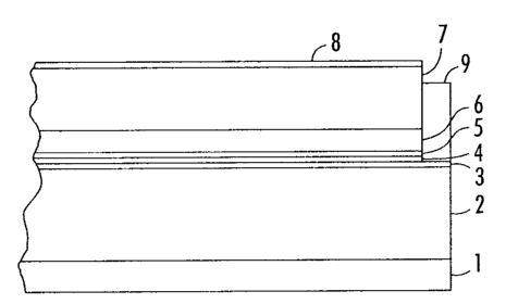
[0018] FIG. 2 represents a simplified side view of an exemplary
photoreceptor
that incorporates a SOF of the present disclosure.
[0019] FIG. 3 represents a simplified side view of a second exemplary
photoreceptor that incorporates a SOF of the present disclosure.
[0020] FIG. 4 represents a simplified side view of a third exemplary
photoreceptor that incorporates a SOF of the present disclosure.
[0021] Unless otherwise noted, the same reference numeral in different
Figures refers to the same or similar feature.
DETAILED DESCRIPTION
[0022] "Structured organic film" (SOF) refers to a COF that is a film at
a
macroscopic level. The imaging members of the present disclosure may comprise
composite SOFs, which optionally may have a capping unit or group added into
the
SOF.
[0023] In this specification and the claims that follow, singular forms
such as
"a," "an," and "the" include plural forms unless the content clearly dictates
otherwise.
[0024] The tenn "SOF" or "SOF composition" generally refers to a covalent
organic framework (COF) that is a film at a macroscopic level. However, as
used in
the present disclosure the term "SOF" does not encompass graphite, graphene,
and/or
diamond. The phrase "macroscopic level" refers, for example, to the naked eye
view
of the present SOFs. Although COFs are a network at the "microscopic level" or
"molecular level" (requiring use of powerful magnifying equipment or as
assessed
using scattering methods), the present SOF is fundamentally different at the
"macroscopic level" because the film is for instance orders of magnitude
larger in
coverage than a microscopic level COF network. SOFs described herein that may
be
used in the embodiments described herein are solvent resistant and have
macroscopic
morphologies much different than typical COFs previously synthesized.
[0025] The term "fluorinated SOF" refers, for example, to a SOF that
contains
fluorine atoms covalently bonded to one or more segment types or linker types
of the
SOF. The fluorinated SOFs of the present disclosure may further comprise
- 5 -
CA 02790546 2012-09-21
, .
fluorinated molecules that are not covalently bound to the framework of the
SOF, but
are randomly distributed in the fluorinated SOF composition (i.e., a composite
fluorinated SOF). However, an SOF, which does not contain fluorine atoms
covalently bonded to one or more segment types or linker types of the SOF,
that
merely includes fluorinated molecules that are not covalently bonded to one or
more
segments or linkers of the SOF is a composite SOF, not a fluorinated SOF.
[0026] Designing and tuning the fluorine content in the SOF
compositions of
the present disclosure is straightforward and neither requires synthesis of
custom
polymers, nor requires blending/dispersion procedures. Furthermore, the SOF
compositions of the present disclosure may be SOF compositions in which the
fluorine content is uniformly dispersed and patterned at the molecular level.
Fluorine
content in the SOFs of the present disclosure may be adjusted by changing the
molecular building block used for SOF synthesis or by changing the amount of
fluorine building block employed.
[0027] In embodiments, the fluorinated SOF may be made by the
reaction of
one or more suitable molecular building blocks, where at least one of the
molecular
building block segments comprises fluorine atoms.
[0028] In embodiments, the imaging members and/or photoreceptors of
the
present disclosure comprise an outermost layer that comprises a fluorinated
SOF in
which a first segment having hole transport properties, which may or may not
be
obtained from the reaction of a fluorinated building block, may be linked to a
second
segment that is fluorinated, such as a second segment that has been obtained
from the
reaction of a fluorine-containing molecular building block.
[0029] In embodiments, the fluorine content of the fluorinated SOFs
comprised in the imaging members and/or photoreceptors of the present
disclosure
may be homogeneously distributed throughout the SOF. The homogenous
distribution of fluorine content in the SOF comprised in the imaging members
and/or
photoreceptors of the present disclosure may be controlled by the SOF forming
process and therefore the fluorine content may also be patterned at the
molecular
level.
- 6 -
CA 02790546 2012-09-21
[0030] In embodiments, the outermost layer of the imaging members and/or
photoreceptors comprises an SOF wherein the microscopic arrangement of
segments
is patterned. The term "patterning" refers, for example, to the sequence in
which
segments are linked together. A patterned fluorinated SOF would therefore
embody a
composition wherein, for example, segment A (having hole transport molecule
functions) is only connected to segment B (which is a fluorinated segment),
and
conversely, segment B is only connected to segment A.
[0031] In embodiments, the outermost layer of the imaging members and/or
photoreceptors comprises an SOF having only one segment, say segment A (for
example having both hole transport molecule functions and being fluorinated),
is
employed is will be patterned because A is intended to only react with A.
[0032] In principle a patterned SOF may be achieved using any number of
segment types. The patterning of segments may be controlled by using molecular
building blocks whose functional group reactivity is intended to compliment a
partner
molecular building block and wherein the likelihood of a molecular building
block to
react with itself is minimized. The aforementioned strategy to segment
patterning is
non-limiting.
[0033] In embodiments, the outermost layer of the imaging members and/or
photoreceptors comprises patterned fluorinated SOFs having different degrees
of
patterning. For example, the patterned fluorinated SOF may exhibit full
patterning,
which may be detected by the complete absence of spectroscopic signals from
building block functional groups. In other embodiments, the patterned
fluorinated
SOFs having lowered degrees of patterning wherein domains of patterning exist
within the SOF.
[0034] It is appreciated that a very low degree of patterning is
associated with
inefficient reaction between building blocks and the inability to form a film.
Therefore, successful implementation of the process of the present disclosure
requires
appreciable patterning between building blocks within the SOF. The degree of
necessary patterning to form a patterned fluorinated SOF suitable for the
outer layer
of imaging members and/or photoreceptors can depend on the chosen building
blocks
- 7 -
CA 02790546 2012-09-21
and desired linking groups. The minimum degree of patterning required to form
a
suitable patterned fluorinated SOF for the outer layer of imaging members
and/or
photoreceptors may be quantified as formation of about 40 % or more of the
intended
linking groups or about 50 % or more of the intended linking groups; the
nominal
degree of patterning embodied by the present disclosure is formation of about
80 % or
more of the intended linking group, such as formation of about 95 % or more of
the
intended linking groups, or about 100% of the intended linking groups.
Formation of
linking groups may be detected spectroscopically.
[0035] In embodiments, the fluorine content of the fluorinated SOFs
comprised in the outermost layer of the imaging members and/or photoreceptors
of
the present disclosure may be distributed throughout the SOF in a
heterogeneous
manner, including various patterns, wherein the concentration or density of
the
fluorine content is reduced in specific areas, such as to form a pattern of
alternating
bands of high and low concentrations of fluorine of a given width. Such
pattering
maybe accomplished by utilizing a mixture of molecular building blocks sharing
the
same general parent molecular building block structure but differing in the
degree of
fluorination (i.e., the number of hydrogen atoms replaced with fluorine) of
the
building block.
[0036] In embodiments, the SOFs comprised in the outermost layer of the
imaging members and/or photoreceptors of the present disclosure of the present
disclosure may possess a heterogeneous distribution of the fluorine content,
for
example, by the application of highly fluorinated or perfluorinated molecular
building
block to the top of a formed wet layer, which may result in a higher portion
of highly
fluorinated or perfluorinated segments on a given side of the SOF and thereby
forming a heterogeneous distribution highly fluorinated or perfluorinated
segments
within the thickness of the SOF, such that a linear or nonlinear concentration
gradient
may be obtained in the resulting SOF obtained after promotion of the change of
the
wet layer to a dry SOF. In such embodiments, a majority of the highly
fluorinated or
perfluorinated segments may end up in the upper half (which is opposite the
substrate)
of the dry SOF or a majority of the highly fluorinated or perfluorinated
segments may
end up in the lower half (which is adjacent to the substrate) of the dry SOF.
- 8 -
CA 02790546 2012-09-21
[0037] In embodiments, comprised in the outermost layer of the imaging
members and/or photoreceptors of the present disclosure may comprise non-
fluorinated molecular building blocks (which may or may not have hole
transport
molecule functions) that may be added to the top surface of a deposited wet
layer,
which upon promotion of a change in the wet film, results in an SOF having a
heterogeneous distribution of the non-fluorinated segments in the dry SOF. In
such
embodiments, a majority of the non-fluorinated segments may end up in the
upper
half (which is opposite the substrate) of the dry SOF or a majority of the non-
fluorinated segments may end up in the lower half (which is adjacent to the
substrate)
of the dry SOF.
[0038] In embodiments, the fluorine content in the SOF comprised in the
outermost layer of the imaging members and/or photoreceptors of the present
disclosure may be easily altered by changing the fluorinated building block or
the
degree of fluorination of a given molecular building block. For example, the
fluorinated SOF compositions of the present disclosure may be hydrophobic, and
may
also be tailored to possess an enhanced charge transport property by the
selection of
particular segments and/or secondary components.
[0039] In embodiments, the fluorinated SOFs may be made by the reaction
of
one or more molecular building blocks, where at least one of the molecular
building
blocks contains fluorine and at least one at least one of the molecular
building blocks
has charge transport molecule functions (or upon reaction results in a segment
with
hole transport molecule functions. For example, the reaction of at least one,
or two or
more molecular building blocks of the same or different fluorine content and
hole
transport molecule functions may be undertaken to produce a fluorinated SOF.
In
specific embodiments, all of the molecular building blocks in the reaction
mixture
may contain fluorine which may be used as the outermost layer of the imaging
members and/or photoreceptors of the present disclosure. In embodiments, a
different
halogen, such as chlorine, and may optionally be contained in the molecular
building
blocks.
[0040] The fluorinated molecular building blocks may be derived from one
or
more building blocks containing a carbon or silicon atomic core; building
blocks
- 9 -
CA 02790546 2012-09-21
containing alkoxy cores; building blocks containing a nitrogen or phosphorous
atomic
core; building blocks containing aryl cores; building blocks containing
carbonate
cores; building blocks containing carbocyclic-, carbobicyclic-, or
carbotricyclic core;
and building blocks containing an oligothiophene core. Such fluorinated
molecular
building blocks may be derived by replacing or exchanging one or more hydrogen
atoms with a fluorine atom. In embodiments, one or more one or more of the
above
molecular building blocks may have all the carbon bound hydrogen atoms
replaced by
fluorine. In embodiments, one or more one or more of the above molecular
building
blocks may have one or more hydrogen atoms replaced by a different halogen,
such as
by chlorine. In addition to fluorine, the SOFs of the present disclosure may
also
include other halogens, such as chlorine.
[0041] In embodiments, one or more fluorinated molecular building blocks
may be respectively present individually or totally in the fluorinated SOF
comprised
in the outermost layer of the imaging members and/or photoreceptors of the
present
disclosure at a percentage of about 5 to about 100% by weight, such as at
least about
50% by weight, or at least about 75% by weight, in relation to 100 parts by
weight of
the SOF.
[0042] In embodiments, the fluorinated SOF may have greater than about
20%
of the H atoms replaced by fluorine atoms, such as greater than about 50%,
greater
than about 75%, greater than about 80%, greater than about 90%, or greater
than
about 95% of the H atoms replaced by fluorine atoms, or about 100% of the H
atoms
replaced by fluorine atoms.
[0043] In embodiments, the fluorinated SOF may have greater than about
20%, greater than about 50%, greater than about 75%, greater than about 80%,
greater
than about 90%, greater than about 95%, or about 100% of the C-bound H atoms
replaced by fluorine atoms.
[0044] In embodiments, a significant hydrogen content may also be
present,
e.g. as carbon-bound hydrogen, in the SOFs of the present disclosure. In
embodiments, in relation to the sum of the C-bound hydrogen and C-bound
fluorine
atoms, the percentage of the hydrogen atoms may be tailored to any desired
amount.
- 10-
CA 02790546 2012-09-21
.=
For example the ratio of C-bound hydrogen to C-bound fluorine may be less than
about 10, such as a ratio of C-bound hydrogen to C-bound fluorine of less than
about
5, or a ratio of C-bound hydrogen to C-bound fluorine of less than about 1, or
a ratio
of C-bound hydrogen to C-bound fluorine of less than about 0.1, or a ratio of
C-bound
hydrogen to C-bound fluorine of less than about 0.01.
[0045] In embodiments, the fluorine content of the fluorinated
SOF comprised
in the outermost layer of the imaging members and/or photoreceptors of the
present
disclosure may be of from about 5% to about 75% by weight, such as about 5% to
about 65% by weight, or about 10% to about 50% by weight. In embodiments, the
fluorine content of the fluorinated SOF comprised in the outermost layer of
the
imaging members and/or photoreceptors of the present disclosure is not less
than
about 5% by weight, such as not less than about 10% by weight, or not less
than about
15% by weight, and an upper limit of the fluorine content is about 75% by
weight, or
about 60% by weight.
[0046] In embodiments, the outermost layer of the imaging
members and/or
photoreceptors of the present disclosure may comprise and SOF where any
desired
amount of the segments in the SOF may be fluorinated. For example, the percent
of
fluorine containing segments may be greater than about 10% by weight, such as
greater than about 30% by weight, or greater than 50% by weight; and an upper
limit
percent of fluorine containing segments may be 100%, such as less than about
90% by
weight, or less than about 70% by weight.
[0047] In embodiments, the outermost layer of the imaging
members and/or
photoreceptors of the present disclosure may comprise a first fluorinated
segment and
a second electroactive segment in the SOF of the outermost layer in an amount
greater
than about 80% by weight of the SOF, such as from about 85 to about 99.5
percent by
weight of the SOF, or about 90 to about 99.5 percent by weight of the SOF.
[0048] In embodiments, the fluorinated SOF comprised in the
outermost layer
of the imaging members and/or photoreceptors of the present disclosure may be
a
"solvent resistant" SOF, a patterned SOF, a capped SOF, a composite SOF,
and/or a
- 11 -
CA 02790546 2012-09-21
,=
periodic SOF, which collectively are hereinafter referred to generally as
an "SOF," unless specifically stated otherwise.
[0049] The term "solvent resistant" refers, for example, to
the substantial
absence of (1) any leaching out any atoms and/or molecules that were at one
time
covalently bonded to the SOF and/or SOF composition (such as a composite SOF),
and/or (2) any phase separation of any molecules that were at one time part of
the
SOF and/or SOF composition (such as a composite SOF), that increases the
susceptibility of the layer into which the SOF is incorporated to
solvent/stress
cracking or degradation. The term "substantial absence" refers for example, to
less
than about 0.5% of the atoms and/or molecules of the SOF being leached out
after
continuously exposing or immersing the SOF comprising imaging member (or SOF
imaging member layer) to a solvent (such as, for example, either an aqueous
fluid, or
organic fluid) for a period of about 24 hours or longer (such as about 48
hours, or
about 72 hours), such as less than about 0.1% of the atoms and/or molecules of
the
SOF being leached out after exposing or immersing the SOF comprising to a
solvent
for a period of about 24 hours or longer (such as about 48 hours, or about 72
hours),
or less than about 0.01% of the atoms and/or molecules of the SOF being
leached out
after exposing or immersing the SOF to a solvent for a period of about 24
hours or
longer (such as about 48 hours, or about 72 hours).
[0050] The term "organic fluid" refers, for example, to
organic liquids or
solvents, which may include, for example, alkenes, such as, for example,
straight
chain aliphatic hydrocarbons, branched chain aliphatic hydrocarbons, and the
like,
such as where the straight or branched chain aliphatic hydrocarbons have from
about
1 to about 30 carbon atoms, such as from about 4 to about 20 carbons;
aromatics, such
as, for example, toluene, xylenes (such as o-, m-, p-xylene), and the like
and/or
mixtures thereof; isopar solvents or isoparaffinic hydrocarbons, such as a non-
polar
liquid of the ISOPARTM series, such as ISOPAR E, ISOPAR G, ISOPAR H, ISOPAR
L and ISOPAR M (manufactured by the Exxon Corporation, these hydrocarbon
liquids are considered narrow portions of isoparaffinic hydrocarbon
fractions), the
NORPARTM series of liquids, which are compositions of n-paraffins available
from
Exxon Corporation, the SOLTROLTI" series of liquids available from the
Phillips
- 12 -
CA 02790546 2012-09-21
.=
Petroleum Company, and the SHELLSOLTM series of liquids available from the
Shell
Oil Company, or isoparaffinic hydrocarbon solvents having from about 10 to
about 18
carbon atoms, and or mixtures thereof In embodiments, the organic fluid may be
a
mixture of one or more solvents, i.e., a solvent system, if desired. In
addition, more
polar solvents may also be used, if desired. Examples of more polar solvents
that may
be used include halogenated and nonhalogenated solvents, such as
tetrahydrofuran,
trichloro- and tetrachloroethane, dichloromethane, chloroform,
monochlorobenzene,
acetone, methanol, ethanol, benzene, ethyl acetate, dimethylformamide,
cyclohexanone, N-methyl acetamide and the like. The solvent may be composed of
one, two, three or more different solvents and/or and other various mixtures
of the
above-mentioned solvents.
[0051] When a capping unit is introduced into the SOF, the SOF
framework is
locally 'interrupted' where the capping units are present. These SOF
compositions are
`covalently doped' because a foreign molecule is bonded to the SOF framework
when
capping units are present. Capped SOF compositions may alter the properties of
SOFs without changing constituent building blocks. For example, the mechanical
and
physical properties of the capped SOF where the SOF framework is interrupted
may
differ from that of an uncapped SOF. In embodiments, the capping unit may
fluorinated which would result in a fluorinated SOF.
[0052] The SOFs of the present disclosure may be, at the
macroscopic level,
substantially pinhole-free SOFs or pinhole-free SOFs having continuous
covalent
organic frameworks that can extend over larger length scales such as for
instance
much greater than a millimeter to lengths such as a meter and, in theory, as
much as
hundreds of meters. It will also be appreciated that SOFs tend to have large
aspect
ratios where typically two dimensions of a SOF will be much larger than the
third.
SOFs have markedly fewer macroscopic edges and disconnected external surfaces
than a collection of COP particles.
[0053] In embodiments, a "substantially pinhole-free SOF" or
"pinhole-free
SOF" may be formed from a reaction mixture deposited on the surface of an
underlying substrate. The term "substantially pinhole-free SOF" refers, for
example,
to an SOF that may or may not be removed from the underlying substrate on
which it
- 13 -
CA 02790546 2014-06-05
was formed and contains substantially no pinholes, pores or gaps greater than
the
distance between the cores of two adjacent segments per square cm; such as,
for
example, less than 10 pinholes, pores or gaps greater than about 250
nanometers in
diameter per cm2, or less than 5 pinholes, pores or gaps greater than about
100
nanometers in diameter per cm2. The term "pinhole-free SOF" refers, for
example, to
an SOF that may or may not be removed from the underlying substrate on which
it
was formed and contains no pinholes, pores or gaps greater than the distance
between
the cores of two adjacent segments per micron2, such as no pinholes, pores or
gaps
greater than about 500 Angstroms in diameter per micron2, or no pinholes,
pores or
gaps greater than about 250 Angstroms in diameter per micron2, or no pinholes,
pores
or gaps greater than about 100 Angstroms in diameter per micron2.
100541 A
description of various exemplary molecular building blocks, linkers,
SOF types, capping groups, strategies to synthesize a specific SOF type with
exemplary chemical structures, building blocks whose symmetrical elements are
outlined, and classes of exemplary molecular entities and examples of members
of
each class that may serve as molecular building blocks for SOFs are detailed
in U.S.
Patent Application Serial Nos. 12/716,524; 12/716,449; 12/716,706; 12/716,324;
12/716,686; 12/716,571; 12/815,688; 12/845,053; 12/845,235; 12/854,962;
12/854,957; and 12/845,052 entitled "Structured Organic Films," "Structured
Organic
Films Having an Added Functionality," "Mixed Solvent Process for Preparing
Structured Organic Films," "Composite Structured Organic Films," "Process For
Preparing Structured Organic Films (SOFs) Via a Pre-SOF," "Electronic Devices
Comprising Structured Organic Films," "Periodic Structured Organic Films,"
"Capped
Structured Organic Film Compositions," "Imaging Members Comprising Capped
Structured Organic Film Compositions," "Imaging Members for Ink-Based Digital
Printing Comprising Structured Organic Films," "Imaging Devices Comprising
Structured Organic Films," and "Imaging Members Comprising Structured Organic
Films," respectively; and U.S. Provisional Application No. 61/157,411,
entitled
"Structured Organic Films" filed March 4, 2009.
- 14-
CA 02790546 2014-06-05
[0055] In embodiments, fluorinated molecular building blocks may be
obtained from the fluorination of any of the above "parent" non-fluorinated
molecular
building blocks (e.g., molecular building blocks detailed in U.S. Patent
Application
Serial Nos. 12/716,524; 12/716,449; 12/716,706; 12/716,324; 12/716,686;
12/716,571; 12/815,688; 12/845,053; 12/845,235; 12/854,962; 12/854,957; and
12/845,052. For example, "parent" non-fluorinated molecular building blocks
may be
fluorinated via elemental fluorine at elevated temperatures, such as greater
than about
150 C, or by other known process steps to form a mixture of fluorinated
molecular
building blocks having varying degrees of fluorination, which may be
optionally
purified to obtain an individual fluorinated molecular building block.
Alternatively,
fluorinated molecular building blocks may be synthesized and/or obtained by
simple
purchase of the desired fluorinated molecular building block. The conversion
of a
"parent" non-fluorinated molecular building block into a fluorinated molecular
building block may take place under reaction conditions that utilize a single
set or
range of known reaction conditions, and may be a known one step reaction or
known
multi-step reaction. Exemplary reactions may include one or more known
reaction
mechanisms, such as an addition and/or an exchange.
[0056] For example, the conversion of a parent non-fluorinated molecular
building block into a fluorinated molecular building block may comprise
contacting a
non-fluorinated molecular building block with a known dehydrohalogenation
agent to
produce a fluorinated molecular building block. In embodiments, the
dehydrohalogenation step may be carried out under conditions effective to
provide a
conversion to replace at least about SO% of the H atoms, such as carbon-bound
hydrogens, by fluorine atoms, such as greater than about 60%, greater than
about
75%, greater than about 80%, greater than about 90%, or greater than about 95%
of
the H atoms, such as carbon-bound hydrogens, replaced by fluorine atoms, or
about
100% of the H atoms replaced by fluorine atoms, in non-fluorinated molecular
building block with fluorine. In embodiments, the dehydrohalogenation step may
be
carried out under conditions effective to provide a conversion that replaces
at least
about 99% of the hydrogens, such as carbon-bound hydrogens, in non-fluorinated
- 15-
CA 02790546 2012-09-21
. =
molecular building block with fluorine. Such a reaction may be carried out in
the
liquid phase or in the gas phase, or in a combination of gas and liquid
phases, and it is
contemplated that the reaction can be carried out batch wise, continuous, or a
combination of these. Such a reaction may be carried out in the presence of
catalyst,
such as activated carbon. Other catalysts may be used, either alone or in
conjunction
one another or depending on the requirements of particular molecular building
block
being fluorinated, including for example palladium-based catalyst, platinum-
based
catalysts, rhodium-based catalysts and ruthenium-based catalysts.
[0057] Molecular Building Block
[0058] The SOFs of the present disclosure comprise molecular
building
blocks having a segment (S) and functional groups (Fg). Molecular building
blocks
require at least two functional groups (x 2) and may comprise a single type or
two
or more types of functional groups. Functional groups are the reactive
chemical
moieties of molecular building blocks that participate in a chemical reaction
to link
together segments during the SOF forming process. A segment is the portion of
the
molecular building block that supports functional groups and comprises all
atoms that
are not associated with functional groups. Further, the composition of a
molecular
building block segment remains unchanged after SOF formation.
[0059] Molecular Building Block Symmetry
100601 Molecular building block symmetry relates to the positioning
of
functional groups (Fgs) around the periphery of the molecular building block
segments. Without being bound by chemical or mathematical theory, a symmetric
molecular building block is one where positioning of Fgs may be associated
with the
ends of a rod, vertexes of a regular geometric shape, or the vertexes of a
distorted rod
or distorted geometric shape. For example, the most symmetric option for
molecular
building blocks containing four Fgs are those whose Fgs overlay with the
corners of a
square or the apexes of a tetrahedron.
[0061] Use of symmetrical building blocks is practiced in
embodiments of the
present disclosure for two reasons: (1) the patterning of molecular building
blocks
may be better anticipated because the linking of regular shapes is a better
understood
- 16-
CA 02790546 2012-09-21
process in reticular chemistry, and (2) the complete reaction between
molecular
building blocks is facilitated because for less symmetric building blocks
errant
conformations/orientations may be adopted which can possibly initiate numerous
linking defects within SOFs.
[0062] FIGS. 1A-0 illustrate exemplary building blocks whose symmetrical
elements are outlined. Such symmetrical elements are found in building blocks
that
may be used in the present disclosure. Such exemplary building blocks may or
may
not be fluorinated.
[0063] Non-limiting examples of various classes of exemplary molecular
entities, which may or may not be fluorinated, that may serve as molecular
building
blocks for SOFs of the present disclosure include building blocks containing a
carbon
or silicon atomic core; building blocks containing alkoxy cores; building
blocks
containing a nitrogen or phosphorous atomic core; building blocks containing
aryl
cores; building blocks containing carbonate cores; building blocks containing
carbocyclic-, carbobicyclic-, or carbotricyclic core; and building blocks
containing an
oligothiophene core.
100641 In embodiments, exemplary fluorinated molecular building blocks
may
be obtained from the fluorination building blocks containing a carbon or
silicon
atomic core; building blocks containing alkoxy cores; building blocks
containing a
nitrogen or phosphorous atomic core; building blocks containing aryl cores;
building
blocks containing carbonate cores; building blocks containing carbocyclic-,
carbobicyclic-, or carbotricyclic core; and building blocks containing an
oligothiopbene core. Such fluorinated molecular building blocks may be
obtained
from the fluorination of a non-fluorinated molecular building block with
elemental
fluorine at elevated temperatures, such as greater than about 150 C, or by
other
known process steps, or by simple purchase of the desired fluorinated
molecular
building block.
[0065] In embodiments, the Type 1 SOF contains segments (which may be
fluorinated), which are not located at the edges of the SOF, that are
connected by
linkers to at least three other segments. For example, in embodiments the SOF
- 17-
CA 02790546 2012-09-21
-
comprises at least one symmetrical building block selected from the group
consisting
of ideal triangular building blocks, distorted triangular building blocks,
ideal
tetrahedral building blocks, distorted tetrahedral building blocks, ideal
square building
blocks, and distorted square building blocks.
[0066] In embodiments, Type 2 and 3 SOF contains at least one segment
type
(which may or may not be fluorinated), which are not located at the edges of
the SOF,
that are connected by linkers to at least three other segments (which may or
may not
be fluorinated). For example, in embodiments the SOF comprises at least one
symmetrical building block selected from the group consisting of ideal
triangular
building blocks, distorted triangular building blocks, ideal tetrahedral
building blocks,
distorted tetrahedral building blocks, ideal square building blocks, and
distorted
square building blocks.
[0067] Functional Group
[0068] Functional groups are the reactive chemical moieties of
molecular
building blocks that participate in a chemical reaction to link together
segments
during the SOF forming process. Functional groups may be composed of a single
atom, or functional groups may be composed of more than one atom. The atomic
compositions of functional groups are those compositions normally associated
with
reactive moieties in chemical compounds. Non-limiting examples of functional
groups include halogens, alcohols, ethers, ketones, carboxylic acids, esters,
carbonates, amines, amides, imines, ureas, aldehydes, isocyanates, tosylates,
alkenes,
alkynes and the like.
[0069] Molecular building blocks contain a plurality of chemical
moieties, but
only a subset of these chemical moieties are intended to be functional groups
during
the SOF forming process. Whether or not a chemical moiety is considered a
functional group depends on the reaction conditions selected for the SOF
forming
process. Functional groups (Fg) denote a chemical moiety that is a reactive
moiety,
that is, a functional group during the SOF forming process.
[0070] In the SOF foiming process, the composition of a functional
group will
be altered through the loss of atoms, the gain of atoms, or both the loss and
the gain of
- 18-
CA 02790546 2012-09-21
atoms; or, the functional group may be lost altogether. In the SOF, atoms
previously
associated with functional groups become associated with linker groups, which
are the
chemical moieties that join together segments. Functional groups have
characteristic
chemistries and those of ordinary skill in the art can generally recognize in
the present
molecular building blocks the atom(s) that constitute functional group(s). It
should be
noted that an atom or grouping of atoms that are identified as part of the
molecular
building block functional group may be preserved in the linker group of the
SOF.
Linker groups are described below.
[0071] Capping Unit
[0072] Capping units of the present disclosure are molecules that
'interrupt'
the regular network of covalently bonded building blocks normally present in
an SOF.
Capped SOF compositions are tunable materials whose properties can be varied
through the type and amount of capping unit introduced. Capping units may
comprise
a single type or two or more types of functional groups and/or chemical
moieties.
[0073] In embodiments, the SOF comprises a plurality of segments, where
all
segments have an identical structure, and a plurality of linkers, which may or
may not
have an identical structure, wherein the segments that are not at the edges of
the SOF
are connected by linkers to at least three other segments and/or capping
groups. In
embodiments, the SOF comprises a plurality of segments where the plurality of
segments comprises at least a first and a second segment that are different in
structure,
and the first segment is connected by linkers to at least three other segments
and/or
capping groups when it is not at the edge of the SOF.
[0074] In embodiments, the SOF comprises a plurality of linkers including
at
least a first and a second linker that are different in structure, and the
plurality of
segments either comprises at least a first and a second segment that are
different in
structure, where the first segment, when not at the edge of the SOF, is
connected to at
least three other segments and/or capping groups, wherein at least one of the
connections is via the first linker, and at least one of the connections is
via the second
linker; or comprises segments that all have an identical structure, and the
segments
that are not at the edges of the SOF are connected by linkers to at least
three other
- 19-
CA 02790546 2014-06-05
segments and/or capping groups, wherein at least one of the connections is via
the
first linker, and at least one of the connections is via the second linker.
[0075] Segment
[0076] A segment is the portion of the molecular building block that
supports
functional groups and comprises all atoms that are not associated with
functional
groups. Further, the composition of a molecular building block segment remains
unchanged after SOF formation. In embodiments, the SOF may contain a first
segment having a structure the same as or different from a second segment. In
other
embodiments, the structures of the first and/or second segments may be the
same as or
different from a third segment, forth segment, fifth segment, etc. A segment
is also
the portion of the molecular building block that can provide an inclined
property.
Inclined properties are described later in the embodiments.
[0077] The SOF of the present disclosure comprise a plurality of segments
including at least a first segment type and a plurality of linkers including
at least a
first linker type arranged as a covalent organic framework (COF) having a
plurality of
pores, wherein the first segment type and/or the first linker type comprises
at least one
atom that is not carbon. In embodiments, the segment (or one or more of the
segment
types included in the plurality of segments making up the SOF) of the SOF
comprises
at least one atom of an element that is not carbon, such as where the
structure of the
segment comprises at least one atom selected from the group consisting of
hydrogen,
oxygen, nitrogen, silicon, phosphorous, selenium, fluorine, boron, and sulfur.
[0078] A description of various exemplary molecular building blocks,
linkers,
SOF types, strategies to synthesize a specific SOF type with exemplary
chemical
structures, building blocks whose symmetrical elements are outlined, and
classes of
exemplary molecular entities and examples of members of each class that may
serve
as molecular building blocks thr SOFs are detailed in U.S. Patent Application
Serial
Nos. 12/716,524; 12/716,449; 12/716,706; 12/716,324; 12/716,686; 12/716,571;
12/815,688; 12/845,053; 12/845,235; 12/854,962; 12/854,957; 12/845,052,
13/042,950, 13/173,948, 13/181,761, 13/181,912, 13/174,046, and 13/182,047.
- 20-
CA 02790546 2012-09-21
,
100791 Linker
100801 A linker is a chemical moiety that emerges in a SOF upon
chemical
reaction between functional groups present on the molecular building blocks
and/or
capping unit.
[00811 A linker may comprise a covalent bond, a single atom, or a
group of
covalently bonded atoms. The frontier is defined as a covalent bond linker and
may
be, for example, a single covalent bond or a double covalent bond and emerges
when
functional groups on all partnered building blocks are lost entirely. The
latter linker
type is defined as a chemical moiety linker and may comprise one or more atoms
bonded together by single covalent bonds, double covalent bonds, or
combinations of
the two. Atoms contained in linking groups originate from atoms present in
functional groups on molecular building blocks prior to the SOF forming
process.
Chemical moiety linkers may be well-known chemical groups such as, for
example,
esters, ketones, amides, imines, ethers, urethanes, carbonates, and the like,
or
derivatives thereof.
100821 For example, when two hydroxyl (-OH) functional groups are
used to
connect segments in a SOF via an oxygen atom, the linker would be the oxygen
atom,
which may also be described as an ether linker. In embodiments, the SOF may
contain a first linker having a structure the same as or different from a
second linker.
In other embodiments, the structures of the first and/or second linkers may be
the
same as or different from a third linker, etc.
[00831 The SOF of the present disclosure comprise a plurality of
segments
including at least a first segment type and a plurality of linkers including
at least a
first linker type arranged as a covalent organic framework (COF) having a
plurality of
pores, wherein the first segment type and/or the first linker type comprises
at least one
atom that is not carbon. In embodiments, the linker (or one or more of the
plurality of
linkers) of the SOF comprises at least one atom of an element that is not
carbon, such
as where the structure of the linker comprises at least one atom selected from
the
group consisting of hydrogen, oxygen, nitrogen, silicon, phosphorous,
selenium,
fluorine, boron, and sulfur.
-21 -
CA 02790546 2012-09-21
[0084] Metrical Parameters of SOFs
[0085] SOFs have any suitable aspect ratio. In embodiments, SOFs have
aspect ratios for instance greater than about 30:1 or greater than about 50:1,
or greater
than about 70:1, or greater than about 100:1, such as about 1000:1. The aspect
ratio
of a SOF is defined as the ratio of its average width or diameter (that is,
the dimension
next largest to its thickness) to its average thickness (that is, its shortest
dimension).
The term 'aspect ratio,' as used here, is not bound by theory. The longest
dimension
of a SOF is its length and it is not considered in the calculation of SOF
aspect ratio.
[0086] Generally, SOFs have widths and lengths, or diameters greater than
about 500 micrometers, such as about 10 mm, or 30 mm. The SOFs have the
following illustrative thicknesses: about 10 Angstroms to about 250 Angstroms,
such
as about 20 Angstroms to about 200 Angstroms, for a mono-segment thick layer
and
about 20 nm to about 5 mm, about 50 nm to about 10 mm for a multi-segment
thick
layer.
[0087] SOF dimensions may be measured using a variety of tools and
methods. For a dimension about 1 micrometer or less, scanning electron
microscopy
is the preferred method. For a dimension about 1 micrometer or greater, a
micrometer
(or ruler) is the preferred method.
[0088] Multilayer SOFs
[0089] A SOF may comprise a single layer or a plurality of layers (that
is,
two, three or more layers). SOFs that are comprised of a plurality of layers
may be
physically joined (e.g., dipole and hydrogen bond) or chemically joined.
Physically
attached layers are characterized by weaker interlayer interactions or
adhesion;
therefore physically attached layers may be susceptible to delamination from
each
other. Chemically attached layers are expected to have chemical bonds (e.g.,
covalent
or ionic bonds) or have numerous physical or intermolecular (supramolecular)
entanglements that strongly link adjacent layers.
[0090] In the embodiments, the SOF may be a single layer (mono-segment
thick or multi-segment thick) or multiple layers (each layer being mono-
segment thick
or multi-segment thick). "Thickness" refers, for example, to the smallest
dimension
- 22 -
CA 02790546 2012-09-21
. =
of the film. As discussed above, in a SOF, segments are molecular units that
are
covalently bonded through linkers to generate the molecular framework of the
film.
The thickness of the film may also be defined in terms of the number of
segments that
is counted along that axis of the film when viewing the cross-section of the
film. A
"monolayer" SOF is the simplest case and refers, for example, to where a film
is one
segment thick. A SOF where two or more segments exist along this axis is
referred to
as a "multi-segment" thick SOF.
100911 Practice of Linking Chemistry
100921 In embodiments linking chemistry may occur wherein the
reaction
between functional groups produces a volatile byproduct that may be largely
evaporated or expunged from the SOF during or after the film forming process
or
wherein no byproduct is formed. Linking chemistry may be selected to achieve a
SOF for applications where the presence of linking chemistry byproducts is not
desired. Linking chemistry reactions may include, for example, condensation,
addition/elimination, and addition reactions, such as, for example, those that
produce
esters, imines, ethers, carbonates, urethanes, amides, acetals, and silyl
ethers.
[00931 In embodiments the linking chemistry via a reaction
between function
groups producing a non-volatile byproduct that largely remains incorporated
within
the SOF after the film forming process. Linking chemistry in embodiments may
be
selected to achieve a SOF for applications where the presence of linking
chemistry
byproducts does not impact the properties or for applications where the
presence of
linking chemistry byproducts may alter the properties of a SOF (such as, for
example,
the electroactive, hydrophobic or hydrophilic nature of the SOF). Linking
chemistry
reactions may include, for example, substitution, metathesis, and metal
catalyzed
coupling reactions, such as those that produce carbon-carbon bonds.
[0094] For all linking chemistry the ability to control the
rate and extent of
reaction between building blocks via the chemistry between building block
functional
groups is an important aspect of the present disclosure. Reasons for
controlling the
rate and extent of reaction may include adapting the film forming process for
different
- 23 -
CA 02790546 2012-09-21
coating methods and tuning the microscopic arrangement of building blocks to
achieve a periodic SOF, as defined in earlier embodiments.
[0095] Innate Properties of COFs
[0096] COFs have innate properties such as high thermal stability
(typically
higher than 400 C under atmospheric conditions); poor solubility in organic
solvents
(chemical stability), and porosity (capable of reversible guest uptake). In
embodiments, SOFs may also possess these innate properties.
[0097] Added Functionality of SOFs
[0098] Added functionality denotes a property that is not inherent to
conventional COFs and may occur by the selection of molecular building blocks
wherein the molecular compositions provide the added functionality in the
resultant
SOF. Added functionality may arise upon assembly of molecular building blocks
having an "inclined property" for that added functionality. Added
functionality may
also arise upon assembly of molecular building blocks having no "inclined
property"
for that added functionality but the resulting SOF has the added functionality
as a
consequence of linking segments (S) and linkers into a SOF. Furthermore,
emergence
of added functionality may arise from the combined effect of using molecular
building blocks bearing an "inclined property" for that added functionality
whose
inclined property is modified or enhanced upon linking together the segments
and
linkers into a SOF.
100991 An Inclined Property of a Molecular Building Block
[00100] The term "inclined property" of a molecular building block refers,
for
example, to a property known to exist for certain molecular compositions or a
property that is reasonably identifiable by a person skilled in art upon
inspection of
the molecular composition of a segment. As used herein, the terms "inclined
property" and "added functionality" refer to the same general property (e.g.,
hydrophobic, electroactive, etc.) but "inclined property" is used in the
context of the
molecular building block and "added functionality" is used in the context of
the SOF,
which may be comprised in the outermost layer of the imaging members and/or
photoreceptors of the present disclosure.
- 24 -
CA 02790546 2012-09-21
=
1001011 The hydrophobic (superhydrophobic), hydrophilic, lipophobic
(superlipophobic), lipophilic, photochromic and/or electroactive (conductor,
semiconductor, charge transport material) nature of an SOF are some examples
of the
properties that may represent an "added functionality" of an SOF. These and
other
added functionalities may arise from the inclined properties of the molecular
building
blocks or may arise from building blocks that do not have the respective added
functionality that is observed in the SOF.
1001021 The term hydrophobic (superhydrophobic) refers, for example,
to the
property of repelling water, or other polar species, such as methanol, it also
means an
inability to absorb water and/or to swell as a result. Furthermore,
hydrophobic
implies an inability to form strong hydrogen bonds to water or other hydrogen
bonding species. Hydrophobic materials are typically characterized by having
water
contact angles greater than 90 as measured using a contact angle goniometer
or
related device. Highly hydrophobic as used herein can be described as when a
droplet
of water forms a high contact angle with a surface, such as a contact angle of
from
about 1300 to about 180 . Superhydrophobic as used herein can be described as
when
a droplet of water forms a high contact angle with a surface, such as a
contact angle of
greater than about 150 , or from greater about 150 to about 180 .
[001031 Superhydrophobic as used herein can be described as when a
droplet of
water forms a sliding angle with a surface, such as a sliding angle of from
about 1 to
less than about 30 , or from about 1 to about 25 , or a sliding angle of less
than about
15 , or a sliding angle of less than about 10 .
[001041 The term hydrophilic refers, for example, to the property of
attracting,
adsorbing, or absorbing water or other polar species, or a surface.
Hydrophilicity may
also be characterized by swelling of a material by water or other polar
species, or a
material that can diffuse or transport water, or other polar species, through
itself.
Hydrophilicity, is further characterized by being able to form strong or
numerous
hydrogen bonds to water or other hydrogen bonding species.
[00105] The term lipophobic (oleophobic) refers, for example, to the
property
of repelling oil or other non-polar species such as alkanes, fats, and waxes.
- 25 -
CA 02790546 2012-09-21
=
Lipophobic materials are typically characterized by having oil contact angles
greater
than 900 as measured using a contact angle goniometer or related device. In
the
present disclosure, the term oleophobic refers, for example, to wettability of
a surface
that has an oil contact angle of approximately about 550 or greater, for
example, with
UV curable ink, solid ink, hexadecane, dodecane, hydrocarbons, etc. Highly
oleophobic as used herein can be described as when a droplet of hydrocarbon-
based
liquid, for example, hexadecane or ink, forms a high contact angle with a
surface,
such as a contact angle of from about 130 or greater than about 1300 to about
175
or from about 135 to about 170 . Superoleophobic as used herein can be
described as when a droplet of hydrocarbon-based liquid, for example, ink,
forms a
high contact-angle with a surface, such as a contact angle that is greater
than 150 ,
or from greater than about 150 to about 175 , or from greater than about 150
to
about 160 .
[00106] Superoleophobic as used herein can also be described as when
a
droplet of a hydrocarbon-based liquid, for example, hexadecane, forms a
sliding
angle with a surface of from about 1 to less than about 30 , or from about 1
to
less than about 25 , or a sliding angle of less than about 25 , or a sliding
angle of
less than about 15 , or a sliding angle of less than about 10 .
[00107] The telin lipophilic (oleophilic) refers, for example, to the
property
attracting oil or other non-polar species such as alkanes, fats, and waxes or
a surface
that is easily wetted by such species. Lipophilic materials are typically
characterized
by having a low to nil oil contact angle as measured using, for example, a
contact
angle goniometer. Lipophilicity can also be characterized by swelling of a
material
by hexane or other non-polar liquids.
1001081 Various methods a available for quantifying the wetting or
contact
angle. For example, the wetting can be measured as contact angle, which is
formed
by the substrate and the tangent to the surface of the liquid droplet at the
contact
point. Specifically, the contact angle may be measured using Fibro DAT1100.
The
contact angle determines the interaction between a liquid and a substrate. A
drop of a
specified volume of fluid may be automatically applied to the specimen surface
using
a micro-pipette. Images of the drop in contact with the substrate are captured
by a
- 26 -
CA 02790546 2012-09-21
,
video camera at specified time intervals. The contact angle between the drop
and the
substrate are determined by image analysis techniques on the images captured.
The
rate of change of the contact angles are calculated as a function of time.
[00109] SOFs with hydrophobic added functionality may be prepared by
using
molecular building blocks with inclined hydrophobic properties and/or have a
rough,
textured, or porous surface on the sub-micron to micron scale. A paper
describing
materials having a rough, textured, or porous surface on the sub-micron to
micron
scale being hydrophobic was authored by Cassie and Baxter (Cassie, A. B. D.;
Baxter,
S. Trans. Faraday Soc., 1944, 40, 546).
1001101 Fluorine-containing polymers are known to have lower surface
energies than the corresponding hydrocarbon polymers. For example,
polytetrafluoroethylene (PTFE) has a lower surface energy than polyethylene
(20
mN/m vs 35.3 mN/m). The introduction of fluorine into SOFs, particularly when
fluorine is present at the surface the outermost layer of the imaging members
and/or
photoreceptors of the present disclosure, may be used to modulate the surface
energy
of the SOF compared to the corresponding, non-fluorinated SOF. In most cases,
introduction of fluorine into the SOF will lower the surface energy of the
outermost
layer of the imaging members and/or photoreceptors of the present disclosure.
The
extent the surface energy of the SOF is modulated, may, for example, depend on
the
degree of fluorination and/or the patterning of fluorine at the surface of the
SOF
and/or within the bulk of the SOF. The degree of fluorination and/or the
patterning of
fluorine at the surface of the SOF are parameters that may be tuned by the
processes
of the present disclosure.
[00111] Molecular building blocks comprising or bearing highly-
fluorinated
segments have inclined hydrophobic properties and may lead to SOFs with
hydrophobic added functionality. Highly-fluorinated segments are defined as
the
number of fluorine atoms present on the segment(s) divided by the number of
hydrogen atoms present on the segment(s) being greater than one. Fluorinated
segments, which are not highly-fluorinated segments may also lead to SOFs with
hydrophobic added functionality.
- 27 -
CA 02790546 2012-09-21
. =
[00112] As discussed above, the fluorinated SOFs comprised in
the outermost
layer of the imaging members and/or photoreceptors of the present disclosure
may be
made from versions of any of the molecular building blocks, segments, and/or
linkers
wherein one or more hydrogen(s) in the molecular building blocks are replaced
with
fluorine.
[00113] The above-mentioned fluorinated segments may include,
for example,
a,co-fluoroalkyldiols of the general structure:
\FJn
where n is an integer having a value of 1 or more, such as of from 1 to about
100, or 1
to about 60, or about 2 to about 30, or about 4 to about 10; or fluorinated
alcohols of
the general structure HOCH2(CF2)nCH2OH and their corresponding dicarboxylic
acids
and aldehydes, where n is an integer having a value of 1 or more, such as of
from 1 to
about 100, or 1 to about 60, or about 2 to about 30, or about 4 to about 10;
tetrafluorohydroquinone; perfluoroadipic acid hydrate, 4,4'-
(hexafluoroisopropylidene)diphthalic anhydride; 4,4'-
(hexafluoroisopropylidene)diphenol, and the like.
[00114] SOFs having a rough, textured, or porous surface on the
sub-micron to
micron scale may also be hydrophobic. The rough, textured, or porous SOF
surface
can result from dangling functional groups present on the film surface or from
the
structure of the SOF. The type of pattern and degree of patterning depends on
the
geometry of the molecular building blocks and the linking chemistry
efficiency. The
feature size that leads to surface roughness or texture is from about 100 nm
to about
kun, such as from about 500 nm to about 5 kim.
[00115] The term electroactive refers, for example, to the
property to transport
electrical charge (electrons and/or holes). Electroactive materials include
conductors,
semiconductors, and charge transport materials. Conductors are defined as
materials
that readily transport electrical charge in the presence of a potential
difference.
Semiconductors are defined as materials do not inherently conduct charge but
may
- 28 -
CA 02790546 2012-09-21
become conductive in the presence of a potential difference and an applied
stimuli,
such as, for example, an electric field, electromagnetic radiation, heat, and
the like.
Charge transport materials are defined as materials that can transport charge
when
charge is injected from another material such as, for example, a dye, pigment,
or
metal in the presence of a potential difference.
[00116] Fluorinated SOFs with electroactive added functionality (or hole
transport molecule functions) comprised in outermost layer of the imaging
members
and/or photoreceptors of the present disclosure may be prepared by folining a
reaction
mixture containing the fluorinated molecular building blocks discussed and
molecular
building blocks with inclined electroactive properties and/or molecular
building
blocks that become electroactive as a result of the assembly of conjugated
segments
and linkers. The following sections describe molecular building blocks with
inclined
hole transport properties, inclined electron transport properties, and
inclined
semiconductor properties.
[00117] Conductors may be further defined as materials that give a signal
using
a potentiometer from about 0.1 to about 107 S/cm.
[00118] Semiconductors may be further defined as materials that give a
signal
using a potentiometer from about 10-6 to about 104 S/cm in the presence of
applied
stimuli such as, for example an electric field, electromagnetic radiation,
heat, and the
like. Alternatively, semiconductors may be defined as materials having
electron
and/or hole mobility measured using time-of-flight techniques in the range of
10-10 to
about 106 cm2V1s-1 when exposed to applied stimuli such as, for example an
electric
field, electromagnetic radiation, heat, and the like.
[00119] Charge transport materials may be further defined as materials
that
have electron and/or hole mobility measured using time-of-flight techniques in
the
range of 10-10 to about 106 cm2V-Is-1. It should be noted that under some
circumstances charge transport materials may be also classified as
semiconductors.
[00120] In embodiments, fluorinated SOFs with electroactive added
functionality may be prepared by reacting fluorinated molecular building
blocks with
molecular building blocks with inclined electroactive properties and/or
molecular
- 29 -
CA 02790546 2012-09-21
building blocks that result in electroactive segments resulting from the
assembly of
conjugated segments and linkers. In embodiments, the fluorinated SOF comprised
in
the outermost layer of the imaging members and/or photoreceptors of the
present
disclosure may be made by preparing a reaction mixture containing at least one
fluorinated building block and at least one building block having
electroactive
properties, such as hole transport molecule functions, such HTM segments may
those
described below such as N,N,1\11,N'-tetrakis-[(4-hydroxymethyl)pheny1]-
bipheny1-4,4'-
diamine, having a hydroxyl functional group (-OH) and upon reaction results in
a
segment of N,N,N',N'-tetra-(p-tolyl)bipheny1-4,4'-diamine; and/or N,N'-
diphenyl-
N,N'-bis-(3-hydroxypheny1)-bipheny1-4,4'-diamine, having a hydroxyl functional
group (-OH) and upon reaction results in a segment of N,N,N',1\l'-tetraphenyl-
bipheny1-4,4'-diamine. The following sections describe further molecular
building
blocks and/or the resulting segment core with inclined hole transport
properties,
inclined electron transport properties, and inclined semiconductor properties,
that may
be reacted with fluorinated building blocks (described above) to produce the
fluorinated SOF comprised in the outermost layer of the imaging members and/or
photoreceptors of the present disclosure.
1001211 SOFs with hole transport added functionality may be obtained by
selecting segment cores such as, for example, triarylamines, hydrazones (U.S.
Patent
No. 7,202,002 B2 to Tokarski et al.), and enamines (U.S. Patent No. 7,416,824
B2 to
Kondoh et al.) with the following general structures:
Ark Arl Ar3 Ar\ Arl Ar4
C=C
N¨Ar 5 /
N I / C=N¨N
Ar2 N¨Ar4
Ar2 \Ar 4 k Ar2 Ar3
Ar3
triarylamine enamines hydrazones
The segment core comprising a triarylamine being represented by the following
general formula:
Ari / Ar3
N¨Ar5-+-N
Ar2 \ \Ar4)k
- 30 -
CA 02790546 2012-09-21
wherein Ari, Ar2, Ar3, Ar4 and Ar5 each independently represents a substituted
or
unsubstituted aryl group, or Ar5 independently represents a substituted or
unsubstituted arylene group, and k represents 0 or 1, wherein at least two of
Arl, Ar2,
Ar3, Ar4 and Ar5 comprises a Fg (previously defined). Ar5 may be further
defined as,
for example, a substituted phenyl ring, substituted/unsubstituted phenylene,
substituted/unsubstituted monovalently linked aromatic rings such as biphenyl,
terphenyl, and the like, or substituted/unsubstituted fused aromatic rings
such as
naphthyl, anthranyl, phenanthryl, and the like.
[00122] Segment cores comprising arylamines with hole transport added
functionality include, for example, aryl amines such as triphenylamine,
N,N,N',N'-
tetraphenyl-(1,1'-bipheny1)-4,4'-diamine, N,N'-diphenyl-N,N'-bis(3-
methylpheny1)-
(1, 1 '-biphenyl)-4,4'-diamine, N,N'-bis(4-butylpheny1)-N,N'-diphenyl4p-
terpheny1]-
4,4"-diamine; hydrazones such as N-phenyl-N-methyl-3-(9-ethyl)carbazyl
hydrazone
and 4-diethyl amino benzaldehyde-1,2-diphenyl hydrazone; and oxadiazoles such
as
2,5-bis(4-N,N'-diethylaminopheny1)-1,2,4-oxadiazole, stilbenes, and the like.
[00123] The segment core comprising a hydrazone being represented by the
following general formula:
Arl Ar2
O=N-N
At.
wherein Ari, Ar2, and Ar3 each independently represents an aryl group
optionally
containing one or more substituents, and R represents a hydrogen atom, an aryl
group,
or an alkyl group optionally containing a substituent; wherein at least two of
Ari, Ar2,
and Ar3 comprises a Fg (previously defined); and a related oxadiazole being
represented by the following general formula:
N-N
II
µµ
C C
0
wherein Ar and Ari each independently represent an aryl group that comprises a
Fg
(previously defined).
[00124] The segment core comprising an enamine being represented by the
following general formula:
-31 -
CA 02790546 2012-09-21
Ark /R
C=C
/ \
Ar2 N-Ar4
Ar3
wherein Ari, Ar2, Ar3, and Ar4 each independently represents an aryl group
that
optionally contains one or more substituents or a heterocyclic group that
optionally
contains one or more substituents, and R represents a hydrogen atom, an aryl
group,
or an alkyl group optionally containing a substituent; wherein at least two of
Art, Ar2,
Ar3, and Ar4 comprises a Fg (previously defined).
[00125] The SOF may be a p-type semiconductor, n-type semiconductor or
ambipolar semiconductor. The SOF semiconductor type depends on the nature of
the
molecular building blocks. Molecular building blocks that possess an electron
donating property such as alkyl, alkoxy, aryl, and amino groups, when present
in the
SOF, may render the SOF a p-type semiconductor. Alternatively, molecular
building
blocks that are electron withdrawing such as cyano, nitro, fluoro, fluorinated
alkyl,
and fluorinated aryl groups may render the SOF into the n-type semiconductor.
[00126] Similarly, the electroactivity of SOFs prepared by these molecular
building blocks will depend on the nature of the segments, nature of the
linkers, and
how the segments are orientated within the SOF. Linkers that favor preferred
orientations of the segment moieties in the SOF are expected to lead to higher
electroactivity.
[00127] Process for Preparing a Fluorinated Structured Organic
Film (SOF)
[00128] The process for making SOFs of the present disclosure, such as
fluorinated SOFs, typically comprises a number of activities or steps (set
forth below)
that may be performed in any suitable sequence or where two or more activities
are
performed simultaneously or in close proximity in time:
A process for preparing a SOF comprising:
(a) preparing a liquid-containing reaction mixture comprising a plurality of
molecular building blocks, each comprising a segment (where at least one
segment
- 32 -
CA 02790546 2012-09-21
may comprise fluorine and at least one of the resulting segments is
electroactive, such
as an HTM) and a number of functional groups, and optionally a pre-SOF;
(b) depositing the reaction mixture as a wet film;
(c) promoting a change of the wet film including the molecular building
blocks to a dry film comprising the SOF comprising a plurality of the segments
and a
plurality of linkers arranged as a covalent organic framework, wherein at a
macroscopic level the covalent organic framework is a film;
(d) optionally removing the SOF from the substrate to obtain a free-standing
SOF;
(e) optionally processing the free-standing SOF into a roll;
(f) optionally cutting and seaming the SOF into a belt; and
(g) optionally performing the above SOF formation process(es) upon an SOF
(which was prepared by the above SOF formation process(es)) as a substrate for
subsequent SOF formation process(es).
[00129] The process for making capped SOFs and/or composite SOFs typically
comprises a similar number of activities or steps (set forth above) that are
used to
make a non-capped SOF. The capping unit and/or secondary component may be
added during either step a, b or c, depending the desired distribution of the
capping
unit in the resulting SOF. For example, if it is desired that the capping unit
and/or
secondary component distribution is substantially uniform over the resulting
SOF, the
capping unit may be added during step a. Alternatively, if, for example, a
more
heterogeneous distribution of the capping unit and/or secondary component is
desired,
adding the capping unit and/or secondary component (such as by spraying it on
the
film formed during step b or during the promotion step of step c) may occur
during
steps b and c.
[00130] The above activities or steps may be conducted at atmospheric,
super
atmospheric, or subatmospheric pressure. The term "atmospheric pressure" as
used
herein refers to a pressure of about 760 ton. The term "super atmospheric"
refers to
pressures greater than atmospheric pressure, but less than 20 atm. The term
- 33 -
CA 02790546 2012-09-21
"subatmospheric pressure" refers to pressures less than atmospheric pressure.
In an
embodiment, the activities or steps may be conducted at or near atmospheric
pressure.
Generally, pressures of from about 0.1 atm to about 2 atm, such as from about
0.5 atm
to about 1.5 atm, or 0.8 atm to about 1.2 atm may be conveniently employed.
[00131] Process Action A: Preparation of the Liquid-Containing Reaction
Mixture
[00132] The reaction mixture comprises a plurality of molecular building
blocks that are dissolved, suspended, or mixed in a liquid, such building
blocks may
include, for example, at least one fluorinated building block, and at least
one
electroactive building block, such as, for example, N,N,N',N'-tetrakis-[(4-
hydroxymethyl)pheny1]-bipheny1-4,4'-diamine, having a hydroxyl functional
group (-
OH) and a segment of N,N,N',N'-tetra-(p-tolyl)bipheny1-4,4'-diamine, and/or
N,N'-
diphenyl-N,Nr-bis-(3-hydroxypheny1)-bipheny1-4,4'-diamine, having a hydroxyl
functional group (-OH) and a segment of N,N,N',N'-tetraphenyl-bipheny1-4,4'-
diamine. The plurality of molecular building blocks may be of one type or two
or
more types. When one or more of the molecular building blocks is a liquid, the
use of
an additional liquid is optional. Catalysts may optionally be added to the
reaction
mixture to enable SOF formation or modify the kinetics of SOF formation during
Action C described above. Additives or secondary components may optionally be
added to the reaction mixture to alter the physical properties of the
resulting SOF.
[00133] The reaction mixture components (molecular building blocks,
optionally a capping unit, liquid (solvent), optionally catalysts, and
optionally
additives) are combined (such as in a vessel). The order of addition of the
reaction
mixture components may vary; however, typically the catalyst is added last. In
particular embodiments, the molecular building blocks are heated in the liquid
in the
absence of the catalyst to aid the dissolution of the molecular building
blocks. The
reaction mixture may also be mixed, stirred, milled, or the like, to ensure
even
distribution of the formulation components prior to depositing the reaction
mixture as
a wet film.
- 34-
CA 02790546 2012-09-21
[00134] In embodiments, the reaction mixture may be heated prior to being
deposited as a wet film. This may aid the dissolution of one or more of the
molecular
building blocks and/or increase the viscosity of the reaction mixture by the
partial
reaction of the reaction mixture prior to depositing the wet layer. This
approach may
be used to increase the loading of the molecular building blocks in the
reaction
mixture.
[00135] In particular embodiments, the reaction mixture needs to have a
viscosity that will support the deposited wet layer. Reaction mixture
viscosities range
from about 10 to about 50,000 cps, such as from about 25 to about 25,000 cps
or from
about 50 to about 1000 cps.
[00136] The molecular building block and capping unit loading or "loading"
in
the reaction mixture is defined as the total weight of the molecular building
blocks
and optionally the capping units and catalysts divided by the total weight of
the
reaction mixture. Building block loadings may range from about 10 to 50%, such
as
from about 20 to about 40%, or from about 25 to about 30%. The capping unit
loading may also be chosen, so as to achieve the desired loading of the
capping group.
For example, depending on when the capping unit is to be added to the reaction
mixture, capping unit loadings may range, by weight, less than about 30% by
weight
of the total building block loading, such as from about 0.5% to about 20% by
weight
of the total building block loading, or from about 1% to about 10% by weight
of the
total building block loading.
[00137] In embodiments, the theoretical upper limit for capping unit
molecular
building loading in the reaction mixture (liquid SOF formulation) is the molar
amount
of capping units that reduces the number of available linking groups to 2 per
molecular building block in the liquid SOF formulation. In such a loading,
substantial
SOF formation may be effectively inhibited by exhausting (by reaction with the
respective capping group) the number of available linkable functional groups
per
molecular building block. For example, in such a situation (where the capping
unit
loading is in an amount sufficient to ensure that the molar excess of
available linking
groups is less than 2 per molecular building block in the liquid SOF
formulation),
- 35 -
CA 02790546 2012-09-21
oligomers, linear polymers, and molecular building blocks that are fully
capped with
capping units may predominately form instead of an SOF.
[00138] In embodiments, the wear rate of the dry SOF of the imaging
member or a particular layer of the imaging member may be adjusted or
modulated by
selecting a predetermined building block or combination of building block
loading of
the SOF liquid formulation. In embodiments, the wear rate of the imaging
member
may be from about 5 to about 20 nanometers per kilocycle rotation or from
about 7 to
about 12 nanometers per kilocycle rotation in an experimental fixture.
[00139] The wear rate of the dry SOF of the imaging member or a
particular
layer of the imaging member may also be adjusted or modulated by inclusion of
capping unit and/or secondary component with the predetermined building block
or
combination of building block loading of the SOF liquid formulation. In
embodiments, an effective secondary component and/or capping unit and/or
effective
capping unit and/or secondary component concentration in the dry SOF may be
selected to either decrease the wear rate of the imaging member or increase
the wear
rate of the imaging member. In embodiments, the wear rate of the imaging
member
may be decreased by at least about 2% per 1000 cycles, such as by at least
about 5%
per 100 cycles, or at least 10% per 1000 cycles relative to a non-capped SOF
comprising the same segment(s) and linker(s).
[00140] In embodiments, the wear rate of the imaging member may be
increased by at least about 5% per 1000 cycles, such as by at least about 10%
per
1000 cycles, or at least 25% per 1000 cycles relative to a non-capped SOF
comprising
the same segment(s) and linker(s).
[00141] Liquids used in the reaction mixture may be pure liquids, such as
solvents, and/or solvent mixtures. Liquids are used to dissolve or suspend the
molecular building blocks and catalyst/modifiers in the reaction mixture.
Liquid
selection is generally based on balancing the solubility/dispersion of the
molecular
building blocks and a particular building block loading, the viscosity of the
reaction
mixture, and the boiling point of the liquid, which impacts the promotion of
the wet
layer to the dry SOF. Suitable liquids may have boiling points from about 30
to
- 36 -
CA 02790546 2012-09-21
about 300 C, such as from about 65 C to about 250 C, or from about 100 C
to
about 180 C.
[00142] Liquids can include molecule classes such as alkanes (hexane,
heptane,
octane, nonane, decane, cyclohexane, cycloheptane, cyclooctane, decalin);
mixed
alkanes (hexanes, heptanes); branched alkanes (isooctane); aromatic compounds
(toluene, o-, p-xylene, mesitylene, nitrobenzene, benzonitrile,
butylbenzene,
aniline); ethers (benzyl ethyl ether, butyl ether, isoamyl ether, propyl
ether); cyclic
ethers (tetrahydrofuran, dioxane), esters (ethyl acetate, butyl acetate, butyl
butyrate,
ethoxyethyl acetate, ethyl propionate, phenyl acetate, methyl benzoate);
ketones
(acetone, methyl ethyl ketone, methyl isobutylketone, diethyl ketone,
chloroacetone,
2-heptanone), cyclic ketones (cyclopentanone, cyclohexanone), amines (10, 2 ,
or 30
amines such as butylamine, diisopropylamine, triethylamine,
diisoproylethylamine;
pyridine); amides (dimethylformamide, N-methylpyrolidinone, N,N-
dimethylformamide); alcohols (methanol, ethanol, n-, i-propanol, n-, , t-
butanol, 1-
methoxy-2-propanol, hexanol, cyclohexanol, 3-pentanol, benzyl alcohol);
nitriles
(acetonitrile, benzonitrile, butyronitrile), halogenated aromatics
(chlorobenzene,
dichlorobenzene, hexafluorobenzene), halogenated alkanes (dichloromethane,
chloroform, dichloroethylene, tetrachloroethane); and water.
1001431 Mixed liquids comprising a first solvent, second solvent, third
solvent,
and so forth may also be used in the reaction mixture. Two or more liquids may
be
used to aid the dissolution/dispersion of the molecular building blocks;
and/or
increase the molecular building block loading; and/or allow a stable wet film
to be
deposited by aiding the wetting of the substrate and deposition instrument;
and/or
modulate the promotion of the wet layer to the dry SOF. In embodiments, the
second
solvent is a solvent whose boiling point or vapor-pressure curve or affinity
for the
molecular building blocks differs from that of the first solvent. In
embodiments, a
first solvent has a boiling point higher than that of the second solvent. In
embodiments, the second solvent has a boiling point equal to or less than
about
100 C, such as in the range of from about 30 C to about 100 C, or in the range
of
from about 40 C to about 90 C, or about 50 C to about 80 C.
- 37 -
CA 02790546 2012-09-21
[00144] The ratio of the mixed liquids may be established by one skilled
in the
art. The ratio of liquids a binary mixed liquid may be from about 1:1 to about
99:1,
such as from about 1:10 to about 10:1, or about 1:5 to about 5:1, by volume.
When n
liquids are used, with n ranging from about 3 to about 6, the amount of each
liquid
ranges from about 1% to about 95% such that the sum of each liquid
contribution
equals 100%.
[00145] The term "substantially removing" refers to, for example, the
removal
of at least 90% of the respective solvent, such as about 95% of the respective
solvent.
The term "substantially leaving" refers to, for example, the removal of no
more than
2% of the respective solvent, such as removal of no more than 1% of the
respective
solvent.
[00146] These mixed liquids may be used to slow or speed up the rate of
conversion of the wet layer to the SOF in order to manipulate the
characteristics of the
SOFs. For example, in condensation and addition/elimination linking
chemistries,
liquids such as water, 10, 2 , or 3 alcohols (such as methanol, ethanol,
propanol,
isopropanol, butanol, 1-methoxy-2-propanol, tert-butanol) may be used.
[00147] Optionally a catalyst may be present in the reaction mixture to
assist
the promotion of the wet layer to the dry SOF. Selection and use of the
optional
catalyst depends on the functional groups on the molecular building blocks.
Catalysts
may be homogeneous (dissolved) or heterogeneous (undissolved or partially
dissolved) and include Bronsted acids (HC1 (aq), acetic acid, p-
toluenesulfonic acid,
amine-protected p-toluenesulfonic acid such as pyrridium p-toluenesulfonate,
trifluoroacetic acid); Lewis acids (boron trifluoroetherate, aluminum
trichloride);
Bronsted bases (metal hydroxides such as sodium hydroxide, lithium hydroxide,
potassium hydroxide; 10, 2 , or 3 amines such as butylamine,
diisopropylamine,
triethylamine, diisoproylethylamine); Lewis bases (N,N-dimethy1-4-
aminopyridine);
metals (Cu bronze); metal salts (FeC13, AuC13); and metal complexes (ligated
palladium complexes, ligated ruthenium catalysts). Typical catalyst loading
ranges
from about 0.01% to about 25%, such as from about 0.1% to about 5% of the
molecular building block loading in the reaction mixture. The catalyst may or
may
not be present in the final SOF composition.
- 38 -
CA 02790546 2014-06-05
1001481 Optionally additives or secondary components, such as dopants, may
be present in the reaction mixture and wet layer. Such additives or secondary
components may also be integrated into a dry SOF. Additives or secondary
components can be homogeneous or heterogeneous in the reaction mixture and wet
layer or in a dry SOF. In contrast to capping units, the terms "additive" or
"secondary
component," refer, for example, to atoms or molecules that are not covalently
bound
in the SOF, but are randomly distributed in the composition. Suitable
secondary
components and additives are described in U.S. Patent Application Serial No.
12/716,324, entitled "Composite Structured Organic Films".
1001491 In embodiments, the SOF may contain antioxidants as a secondary
component to protect the SOF from oxidation. Examples of suitable antioxidants
include (1) N,N'-hexamethylene bis(3,5-di-tert-buty1-4-hydroxy
hydrocinnamamide)
(IRGANOX 1098, available from Ciba-Geigy Corporation), (2) 2,2-bis(4-(2-(3,5-
di-
tert-buty1-4-hydroxyhydrocinnamoyloxy) )ethoxyphenyl) propane (TOPANOL-205,
available from ICI America Corporation), (3) tris(4-tert-butyl-3-hydroxy-2,6-
dimethyl
benzyl) isocyanurate (CYANOX 1790, 41,322-4, LTDP, Aldrich D12,840-6), (4)
2,2'-
ethylidene bis(4,6-di-tert-butylphenyl) fluoro phosphonite (ETHANOX-398,
available
from Ethyl Corporation), (5) tetrakis(2,4-di-tert-butylpheny1)-4,4'-biphenyl
diphosphonite (ALDRICH 46,852-5; hardness value 90), (6) pentaerythritol
tetrastearate (TCI America #P0739), (7) tributylammonium hypophosphite
(Aldrich
42,009-3), (8) 2,6-di-tert-butyl-4-methoxyphenol (Aldrich 25,106-2), (9) 2,4-
di-tert-
buty1-6-(4-methoxybenzyl) phenol (Aldrich 23,008-1), (10) 4-bromo-2,6-
dimethylphenol (Aldrich 34,951-8), (11) 4-bromo-3,5-didimethylphenol (Aldrich
B6,420-2), (12) 4-bromo-2-nitrophenol (Aldrich 30,987-7), (13) 4-(diethyl
aminomethyl)-2,5-dimethylphenol (Aldrich 14,668-4), (14) 3-dimethylaminophenol
(Aldrich D14,400-2), (15) 2-amino-4-tert-amylphenol (Aldrich 41,258-9), (16)
2,6-
bis(hydroxymethyl)-p-cresol (Aldrich 22,752-8), (17) 2,21-methylenediphenol
(Aldrich B4,680-8), (18) 5-(diethylamino)-2-nitrosophenol (Aldrich 26,951-4),
(19)
2,6-dichloro-4-fluorophenol (Aldrich 28,435-1), (20) 2,6-dibromo fluoro phenol
(Aldrich 26,003-7), (21) a trifluoro-o-cresol (Aldrich 21,979-7), (22) 2-bromo-
4-
- 39 -
CA 02790546 2012-09-21
=
fluorophenol (Aldrich 30,246-5), (23) 4-fluorophenol (Aldrich F1,320-7), (24)
4-
chloropheny1-2-chloro-1,1,2-tri-fluoroethyl sulfone (Aldrich 13,823-1), (25)
3,4-
difluoro phenylacetic acid (Aldrich 29,043-2), (26) 3-fluorophenylacetic acid
(Aldrich
24,804-5), (27) 3,5-difluoro phenylacetic acid (Aldrich 29,044-0), (28) 2-
fluorophenylacetic acid (Aldrich 20,894-9), (29) 2,5-bis (trifluoromethyl)
benzoic
acid (Aldrich 32,527-9), (30) ethyl-2-(4-(4-(trifluoromethyl) phenoxy)
phenoxy)
propionate (Aldrich 25,074-0), (31) tetrakis (2,4-di-tert-butyl phenyl)-4,4'-
biphenyl
diphosphonite (Aldrich 46,852-5), (32) 4-tert-amyl phenol (Aldrich 15,384-2),
(33) 3-
(2H-benzotriazol-2-y1)-4-hydroxy phenethylalcohol (Aldrich 43,071-4), NAUGARD
76, NAUGARD 445, NAUGARD 512, and NAUGARD 524 (manufactured by
Uniroyal Chemical Company), and the like, as well as mixtures thereof.
[00150] In embodiments, the antioxidants that are selected so as to
match the
oxidation potential of the hole transport material. For example, the
antioxidants may
be chosen, for example, from among sterically hindered bis-phenols, sterically
hindered dihydroquinones, or sterically hindered amines. The antioxidants may
be
chosen, for example, from among sterically hindered bis-phenols, sterically
hindered
dihydroquinones, or sterically hindered amines. Exemplary sterically hindered
bis-
phenols may be, for example, 2,2'-methylenebis(4-ethy1-6-tert-butylphenol).
Exemplary sterically hindered dihydroquinones can be, for example, 2,5-di(tert-
amyl)hydroquinone or 4,4'-thiobis(6-tert-butyl-o-cresol and 2,5-di(tert-
amyl)hydroquinone. Exemplary sterically hindered amines can be, for example,
4,4'-
[4-diethylamino)phenyl]methyleneThis(N,N diethyl-3-methylaniline and
bis(1,2,2,6,6-
pentamethy1-4-piperidinyl)(3,5-di-tert-butyl-4-
hydroxybenzyl)butylpropanedioate.
[00151] In embodiments, sterically hindered bis-phenols can be of the
following general structure A-1:
H3C CH3 OH OH H3C
CH3
H2
H3C
CH3
R
R1 2
- 40 -
CA 02790546 2012-09-21
A-1
wherein R1 and R2 are each a hydrogen atom, a halogen atom, or a hydrocarbyl
group
haying from 1 to about 10 carbon atoms, or the following general structure A-
2:
Ri R3
OH
4OH
R2 R4
A-2
wherein R1, R2, R3, and R4 are each a hydrocarbyl group having from 1 to about
10
carbon atoms.
[00152] Exemplary specific sterically hindered his-phenols may be, for
example, 2,2'-inethylenebis(4-ethy1-6-tert-butylphenol) and 2,2'-
methylenebis(4-
methy1-6-tert-butylphenol).
[00153] In embodiments, sterically hindered dihydroquinones can be of the
following general structure A-3:
OH
Ri 10 R2
R3 R4
OH
A-3
wherein R1, R2, R3, and R4 are each a hydrocarbyl group haying from 1 to about
10
carbon atoms.
[00154] Exemplary specific sterically hindered dihydroquinones may be, for
example, 2,5-cli(tert-amyl)hydroquinone, 4,4'-thiobis(6-tert-butyl-o-cresol
and 2,5-
di(tert-amyl)hydroquinone.
-41 -
CA 02790546 2012-09-21
[00155] ln embodiments, sterically hindered amines can be of the following
general structure A-4:
H3C
\C H3
( _________________________________ N __ R1
7CH3
H3C
A-4
wherein R1 is a hydrocarbyl group having from 1 to about 10 carbon atoms.
[00156] Exemplary specific sterically hindered amines may be, for example,
2
uch as 4,4'[4-(diethylamino)phenyl]methylene]bis(N,N diethyl-3-methylaniline
and
bis(1,2,2,6,6-pentamethy1-4-piperidinyl)(3,5-di-tert-butyl-4-
hydroxybenzyl)butylpropanedioate.
[00157] Further examples of antioxidants optionally incorporated into the
charge transport layer or at least one charge transport layer to, for example,
include
hindered phenolic antioxidants, such as tetrakis methylene(3,5-di-tert-buty1-4-
hydroxy
hydrocinnamate) methane (IRGANOX 1010Tm, available from Ciba Specialty
Chemical), butylated hydroxytoluene (BHT), and other hindered phenolic
antioxidants including SUMILIZER BHT-RTm, MDP-STM, BBM-STm, WXRTM,
NWTM, BP76TM, BP-IO1TM, GA-8OTM, GMTm and GSTM (available from Sumitomo
Chemical Co., Ltd.), IRGANOX 1035TM, 1076TM, 1098TM, 1135Tm, 1141Tm, 1222TM,
1330TM, 1425WLTM, I52OLTM, 245TM, 259TM, 3114Tm, 3790TM, 5057TM and 565TM
(available from Ciba Specialties Chemicals), and ADEKA STAB AO-2OTM, AO-
3OTM, AO-4OTM, AO-5OTM, AO-6OTM, AO70TM, AO-8OTM and AO-330TM (available
from Asahi Denka Co., Ltd.); hindered amine antioxidants such as SANOL LS-
2626TM, LS-765TM, LS770TM and LS744TM (available from SNKYO CO., Ltd.),
TINUVIN 144TM and 622LDTM (available from Ciba Specialties Chemicals), MARK
LA57TM, LA67TM, LA62TM, LA68TM and LA63TM (available from Asahi Denka Co.,
Ltd.), and SUMILIZER TPSTm (available from Sumitomo Chemical Co., Ltd.);
-42 -
CA 02790546 2012-09-21
thioether antioxidants such as SUMILIZER TP-DTm (available from Sumitomo
Chemical Co., Ltd); phosphite antioxidants such as MARK 2112Tm, PEP8TM, PEP-
24GTM, PEP36TM, 329KTM and HPl0TM (available from Asahi Denka Co., Ltd.);
other molecules such as bis(4-diethylamino-2-methylphenyl) phenylmethane
(BDETPM), bis-[2-methy1-4-(N-2-hydroxyethyl-N-ethyl-aminopheny1)]-
phenylmethane (DHTPM), and the like.
[00158] The antioxidant, when present, may be present in the SOF composite
in any desired or effective amount, such as up to about 10 percent, or from
about 0.25
percent to about 10 percent by weight of the SOF, or up to about 5 percent,
such as
from about 0.25 percent to about 5 percent by weight of the SOF.
[00159] In embodiments, the outer layer of the imaging member may comprise
further non-hole-transport-molecule segment in addition to the other segments
present
in the SOF that are HTMs, such as a first segment of N,N,Nr,N'-tetra-(p-
tolyl)bipheny1-4,4'-diamine, a second segment of N,N,N',N'-tetraphenyl-
bipheny1-
4,4'-diamine. In such an embodiment, the non-hole-transport-molecule segment
would constitute the third segment in the SOF, and may be a fluorinated
segment. In
embodiments, the SOF may comprise the fluorinated non-hole-transport-molecule
segment, in addition one or more segments with hole-transport properties, such
as a
first segment of N,N,N',N1-tetra-(p-tolyl)bipheny1-4,4'-diamine, and/or a
second
segment of N,N,N',N '-tetraphenyl-biphenyl-4,4'-diamine, among other
additional
segments either with or without hole transport properties (such as a forth,
fifth, sixth,
seventh, etc., segment).
[00160] In embodiments, the reaction mixture may be prepared by including
a
non-hole-transport-molecule segment in addition to the other segment(s). In
such an
embodiment, the non-hole-transport-molecule segment would constitute a third
segment in the SOF. Suitable non-hole-transport-molecule segments include
N,N,N',N',N",N"-hexakis(methylenemethyl)-1,3,5-triazine-2,4,6-triamine:
- 43 -
CA 02790546 2012-09-21
N N
'''= ==== , N,N,N',N',N",N"-hexakis(methoxymethyl)-1,3,5-triazine-
2,4,6-triamine, N,N,N',N',N",N"-hexakis(ethoxymethyl)-1,3,5-triazine-2,4,6-
triamine
and the like. The non-hole-transport-molecule segment, when present, may be
present
in the SOF in any desired amount, such as up to about 30 percent, or from
about 5
percent to about 30 percent by weight of the SOF, or from about 10 percent to
about
25 percent by weight of the SOF.
[00161] Crosslinking secondary components may also be added to the SOF.
Suitable crosslinking secondary components may include melamine monomer or
polymer, benzoguanamine-formaldehyde resins, urea-formaldehyde resins,
glycoluril-
formaldehyde resins, triazine based amino resins and combinations thereof
Typical
amino resins include the melamine resins manufactured by CYTEC such as Cymel
300, 301, 303, 325 350, 370, 380, 1116 and 1130; benzoguananiine resins such
as
Cymel R 1123 and 1125; glycoluril resins such as Cymel 1170, 1171, and 1172
and
urea resins such as CYMEL U-14-160-BX, CYMEL UI-20-E.
[00162] illustrative examples for polymeric and oligomeric type amino
resins
are CYMEL 325, CYMEL 322, CYMEL 3749, CYMEL 3050, CYMEL 1301
melamine based resins, CYMEL U-14-160-BX, CYMEL UI-20-E urea based amino
resins, CYMEL 5010 and benzoguanamine based amino resin and CYMEL 5011
based amino resins, manufactured by CYTEC.
[00163] Monomeric type amino resins may include, for example, CYMEL 300,
CYMEL 303, CYMEL 1135 melamine based resins, CYMEL 1123 benzoguanamine
based amino, CYMEL 1170 and CYMEL 1171 Glycoluril amino resins and Cylink
2000 triazine based amino resin, manufactured by CYTEC.
[00164] in embodiments, the secondary components may have similar or
disparate properties to accentuate or hybridize (synergistic effects or
ameliorative
effects as well as the ability to attenuate inherent or inclined properties of
the capped
- 44 -
CA 02790546 2012-09-21
SOF) the intended property of the SOF to enable it to meet performance
targets. For
example, doping the SOFs with antioxidant compounds will extend the life of
the
SOF by preventing chemical degradation pathways. Additionally, additives maybe
added to improve the morphological properties of the SOF by tuning the
reaction
occurring during the promotion of the change of the reaction mixture to form
the
SOF.
[001651 Process Action B: Depositing the Reaction Mixture as a Wet Film
[00166] The reaction mixture may be applied as a wet film to a variety of
substrates using a number of liquid deposition techniques. The thickness of
the SOF
is dependant on the thickness of the wet film and the molecular building block
loading
in the reaction mixture. The thickness of the wet film is dependent on the
viscosity of
the reaction mixture and the method used to deposit the reaction mixture as a
wet
film.
[00167] Substrates include, for example, polymers, papers, metals and
metal
alloys, doped and undoped forms of elements from Groups III-VI of the periodic
table, metal oxides, metal chalcogenides, and previously prepared SOFs or
capped
SOFs. Examples of polymer film substrates include polyesters, polyolefins,
polycarbonates, polystyrenes, polyvinylchloride, block and random copolymers
thereof, and the like. Examples of metallic surfaces include metallized
polymers,
metal foils, metal plates; mixed material substrates such as metals patterned
or
deposited on polymer, semiconductor, metal oxide, or glass substrates.
Examples of
substrates comprised of doped and undoped elements from Groups III-VI of the
periodic table include, aluminum, silicon, silicon n-doped with phosphorous,
silicon
p-doped with boron, tin, gallium arsenide, lead, gallium indium phosphide, and
indium. Examples of metal oxides include silicon dioxide, titanium dioxide,
indium
tin oxide, tin dioxide, selenium dioxide, and alumina. Examples of metal
chalcogenides include cadmium sulfide, cadmium telluride, and zinc selenide.
Additionally, it is appreciated that chemically treated or mechanically
modified forms
of the above substrates remain within the scope of surfaces which may be
coated with
the reaction mixture.
- 45 -
CA 02790546 2012-09-21
[00168] In embodiments, the substrate may be composed of, for example,
silicon, glass plate, plastic film or sheet. For structurally flexible
devices, a plastic
substrate such as polyester, polycarbonate, polyimide sheets and the like may
be used.
The thickness of the substrate may be from around 10 micrometers to over 10
millimeters with an exemplary thickness being from about 50 to about 100
micrometers, especially for a flexible plastic substrate, and from about 1 to
about 10
millimeters for a rigid substrate such as glass or silicon.
[00169] The reaction mixture may be applied to the substrate using a
number
of liquid deposition techniques including, for example, spin coating, blade
coating,
web coating, dip coating, cup coating, rod coating, screen printing, ink jet
printing,
spray coating, stamping and the like. The method used to deposit the wet layer
depends on the nature, size, and shape of the substrate and the desired wet
layer
thickness. The thickness of the wet layer can range from about 10 nm to about
5 mm,
such as from about 100 nm to about I mm, or from about 1 um to about 500 pm.
[00170] In embodiments, the capping unit and/or secondary component may be
introduced following completion of the above described process action B. The
incorporation of the capping unit and/or secondary component in this way may
be
accomplished by any means that serves to distribute the capping unit and/or
secondary
component homogeneously, heterogeneously, or as a specific pattern over the
wet
film. Following introduction of the capping unit and/or secondary component
subsequent process actions may be carried out resuming with process action C.
[00171] For example, following completion of process action B (i.e., after
the
reaction mixture may be applied to the substrate), capping unit(s) and/or
secondary
components (dopants, additives, etc.) may be added to the wet layer by any
suitable
method, such as by distributing (e.g., dusting, spraying, pouring, sprinkling,
etc,
depending on whether the capping unit and/or secondary component is a
particle,
powder or liquid) the capping unit(s) and/or secondary component on the top
the wet
layer. The capping units and/or secondary components may be applied to the
formed
wet layer in a homogeneous or heterogeneous manner, including various
patterns,
wherein the concentration or density of the capping unit(s) and/or secondary
component is reduced in specific areas, such as to form a pattern of
alternating bands
- 46 -
CA 02790546 2012-09-21
of high and low concentrations of the capping unit(s) and/or secondary
component of
a given width on the wet layer. In embodiments, the application of the capping
unit(s)
and/or secondary component to the top of the wet layer may result in a portion
of the
capping unit(s) and/or secondary component diffusing or sinking into the wet
layer
and thereby forming a heterogeneous distribution of capping unit(s) and/or
secondary
component within the thickness of the SOF, such that a linear or nonlinear
concentration gradient may be obtained in the resulting SOF obtained after
promotion
of the change of the wet layer to a dry SOF. In embodiments, a capping unit(s)
and/or
secondary component may be added to the top surface of a deposited wet layer,
which
upon promotion of a change in the wet film, results in an SOF having an
heterogeneous distribution of the capping unit(s) and/or secondary component
in the
dry SOF. Depending on the density of the wet film and the density of the
capping
unit(s) and/or secondary component, a majority of the capping unit(s) and/or
secondary component may end up in the upper half (which is opposite the
substrate)
of the dry SOF or a majority of the capping unit(s) and/or secondary component
may
end up in the lower half (which is adjacent to the substrate) of the dry SOF.
1001721 Process Action C: Promoting the Change of Wet Film to the Dry
SOF
1001731 The term "promoting" refers, for example, to any suitable
technique to
facilitate a reaction of the molecular building blocks, such as a chemical
reaction of
the functional groups of the building blocks. In the case where a liquid needs
to be
removed to form the dry film, "promoting" also refers to removal of the
liquid.
Reaction of the molecular building blocks (and optionally capping units), and
removal
of the liquid can occur sequentially or concurrently. In embodiments, the
capping
unit and/or secondary component may be added while the promotion of the change
of
the wet film to the dry SOF is occurring. In certain embodiments, the liquid
is also
one of the molecular building blocks and is incorporated into the SOF. The
term "dry
SOF" refers, for example, to substantially dry SOFs (such as capped and/or
composite
SOFs), for example, to a liquid content less than about 5% by weight of the
SOF, or to
a liquid content less than 2% by weight of the SOF.
- 47 -
CA 02790546 2012-09-21
[00174] In embodiments, the dry SOF or a given region of the dry SOF (such
as the surface to a depth equal to of about 10% of the thickness of the SOF or
a depth
equal to of about 5% of the thickness of the SOF, the upper quarter of the
SOF, or the
regions discussed above) the capping units are present in an amount equal to
or
greater than about 0.5%, by mole, with respect to the total moles of capping
units and
segments present, such as from about 1% to about 40%, or from about 2% to 25%
by
mole, with respect to the total moles of capping units and segments present.
For
example when the capping units are present in an amount of about 0.5% by mole
respect to the total moles of capping units and segments present, there would
be about
0.05 mols of capping units and about 9.95 mols of segments present in the
sample.
[00175] Promoting the wet layer to form a dry SOF may be accomplished by
any suitable technique. Promoting the wet layer to form a dry SOF typically
involves
thermal treatment including, for example, oven drying, infrared radiation
(IR), and the
like with temperatures ranging from 40 to 350 C and from 60 to 200 C and from
85 to
160 C. The total heating time can range from about four seconds to about 24
hours,
such as from one minute to 120 minutes, or from three minutes to 60 minutes.
[00176] IR promotion of the wet layer to the COF film may be achieved
using
an IR heater module mounted over a belt transport system. Various types of IR
emitters may be used, such as carbon IR emitters or short wave IR emitters
(available
from Heraerus). Additional exemplary information regarding carbon IR emitters
or
short wave IR emitters is summarized in Table 1 below.
Table 1: Exemplary information regarding carbon or short wave IR emitters
IR lamp Peak Wavelength Number of Module Power
lamps (kW)
Carbon 2.0 micron 2 ¨ twin tube 4.6
Short wave 1.2 ¨ 1.4 micron 3 ¨ twin tube 4.5
- 48 -
CA 02790546 2014-06-05
[00177] Process Action D: Optionally removing the SOF from the coating
substrate to obtain a free-standing SOF
[00178] In embodiments, a free-standing SOF is desired. Free-standing SOFs
may be obtained when an appropriate low adhesion substrate is used to support
the
deposition of the wet layer. Appropriate substrates that have low adhesion to
the SOF
may include, for example, metal foils, metalized polymer substrates, release
papers
and SOFs, such as SOFs prepared with a surface that has been altered to have a
low
adhesion or a decreased propensity for adhesion or attachment. Removal of the
SOF
from the supporting substrate may be achieved in a number of ways by someone
skilled in the art. For example, removal of the SOF from the substrate may
occur by
starting from a corner or edge of the film and optionally assisted by passing
the
substrate and SOF over a curved surface.
[00179] Process Action E: Optionally processing the free-standing SOF
into a roll
[00180] Optionally, a free-standing SOF or a SOF supported by a flexible
substrate may be processed into a roll. The SOF may be processed into a roll
for
storage, handling, and a variety of other purposes. The starting curvature of
the roll is
selected such that the SOF is not distorted or cracked during the rolling
process.
1001811 Process Action F: Optionally cutting and seaming the SOF into a
shape, such as a belt
[00182] The method for cutting and seaming the SOF is similar to that
described in U.S. Patent No. 5,455,136 issued on October 3, 1995 (for polymer
films). An SOF belt may be fabricated from a single SOF, a multi layer SOF or
an
SOF sheet cut from a web. Such sheets may be rectangular in shape or any
particular
shape as desired. All sides of the SOF(s) may be of the same length, or one
pair of
parallel sides may be longer than the other pair of parallel sides. The SOF(s)
may be
fabricated into shapes, such as a belt by overlap joining the opposite
marginal end
regions of the SOF sheet. A seam is typically produced in the overlapping
marginal
end regions at the point of joining. Joining may be affected by any suitable
means.
Typical joining techniques
- 49 -
CA 02790546 2012-09-21
include, for example, welding (including ultrasonic), gluing, taping, pressure
heat
fusing and the like. Methods, such as ultrasonic welding, are desirable
general
methods of joining flexible sheets because of their speed, cleanliness (no
solvents)
and production of a thin and narrow seam.
[00183] Process Action G: Optionally Using a SOF as a Substrate for
Subsequent SOF Formation Processes
[00184] A SOF may be used as a substrate in the SOF folining process to
afford a multi-layered structured organic film. The layers of a multi-layered
SOF may
be chemically bound in or in physical contact. Chemically bound, multi-layered
SOFs are formed when functional groups present on the substrate SOF surface
can
react with the molecular building blocks present in the deposited wet layer
used to
form the second structured organic film layer. Multi-layered SOFs in physical
contact
may not chemically bound to one another.
[00185] A SOF substrate may optionally be chemically treated prior to the
deposition of the wet layer to enable or promote chemical attachment of a
second SOF
layer to form a multi-layered structured organic film.
[00186] Alternatively, a SOF substrate may optionally be chemically
treated
prior to the deposition of the wet layer to disable chemical attachment of a
second
SOF layer (surface pacification) to form a physical contact multi-layered SOF.
[00187] Other methods, such as lamination of two or more SOFs, may also be
used to prepare physically contacted multi-layered SOFs.
1001881 Applications of SOFs in Imaging members, Such as Photoreceptor
Layers
[00189] Representative structures of an electrophotographic imaging member
(e.g., a photoreceptor) are shown in FIGS. 2-4. These imaging members are
provided
with an anti-curl layer 1, a supporting substrate 2, an electrically
conductive ground
plane 3, a charge blocking layer 4, an adhesive layer 5, a charge generating
layer 6, a
charge transport layer 7, an overcoating layer 8, and a ground strip 9. In
FIG. 4,
imaging layer 10 (containing both charge generating material and charge
transport
- 50 -
CA 02790546 2012-09-21
material) takes the place of separate charge generating layer 6 and charge
transport
layer 7.
[00190] As seen in the figures, in fabricating a photoreceptor, a charge
generating material (CGM) and a charge transport material (CTM) may be
deposited
onto the substrate surface either in a laminate type configuration where the
CGM and
CTM are in different layers (e.g., FIGS. 2 and 3) or in a single layer
configuration
where the CGM and CTM are in the same layer (e.g., FIG. 4). In embodiments,
the
photoreceptors may be prepared by applying over the electrically conductive
layer the
charge generation layer 6 and, optionally, a charge transport layer 7. In
embodiments,
the charge generation layer and, when present, the charge transport layer, may
be
applied in either order.
[001911 Anti Curl Layer
1001921 For some applications, an optional anti-curl layer 1, which
comprises
film-forming organic or inorganic polymers that are electrically insulating or
slightly
semi-conductive, may be provided. The anti-curl layer provides flatness and/or
abrasion resistance.
[00193] Anti-curl layer 1 may be formed at the back side of the substrate
2,
opposite the imaging layers. The anti-curl layer may include, in addition to
the film-
forming resin, an adhesion promoter polyester additive. Examples of film-
forming
resins useful as the anti-curl layer include, but are not limited to,
polyacrylate,
polystyrene, poly(4,4'-isopropylidene diphenylcarbonate), poly(4,4'-
cyclohexylidene
diphenylcarbonate), mixtures thereof and the like.
[00194] Additives may be present in the anti-curl layer in the range of
about 0.5
to about 40 weight percent of the anti-curl layer. Additives include organic
and
inorganic particles that may further improve the wear resistance and/or
provide charge
relaxation property. Organic particles include Teflon powder, carbon black,
and
graphite particles. Inorganic particles include insulating and semiconducting
metal
oxide particles such as silica, zinc oxide, tin oxide and the like. Another
semiconducting additive is the oxidized oligomer salts as described in U.S.
Patent No.
-51 -
CA 02790546 2014-06-05
5,853,906. The oligomer salts are oxidized N, N, N', N'-tetra-p-toly1-4,4'-
biphenyldiamine salt.
[00195] Typical adhesion promoters useful as additives include, but are
not
limited to, duPont 49,000 (duPont), Vitel PE-100, Vitel PE-200, Vitel PE-307
(Goodyear), mixtures thereof and the like. Usually from about 1 to about 15
weight
percent adhesion promoter is selected for film-forming resin addition, based
on the
weight of the film-forming resin.
[00196] The thickness of the anti-curl layer is typically from about 3
micrometers to about 35 micrometers, such as from about 10 micrometers to
about 20
micrometers, or about 14 micrometers.
[00197] The anti-curl coating may be applied as a solution prepared by
dissolving the film-forming resin and the adhesion promoter in a solvent such
as
methylene chloride. The solution may be applied to the rear surface of the
supporting
substrate (the side opposite the imaging layers) of the photoreceptor device,
for
example, by web coating or by other methods known in the art. Coating of the
overcoat layer and the anti-curl layer may be accomplished simultaneously by
web
coating onto a multilayer photoreceptor comprising a charge transport layer,
charge
generation layer, adhesive layer, blocking layer, ground plane and substrate.
The wet
film coating is then dried to produce the anti-curl layer 1.
[00198] The Supporting Substrate
[00199] As indicated above, the photoreceptors are prepared by first
providing
a substrate 2, i.e., a support. The substrate may be opaque or substantially
transparent
and may comprise any additional suitable material(s) having given required
mechanical properties, such as those described in U.S. Patent Nos. 4,457,994;
4,871,634; 5,702,854; 5,976,744; and 7,384,717.
[00200] The substrate may comprise a layer of electrically non-conductive
material or a layer of electrically conductive material, such as an inorganic
or organic
composition. If a non-conductive material is employed, it may be necessary to
provide an electrically conductive ground plane over such non-conductive
material. If
- 52 -
CA 02790546 2012-09-21
a conductive material is used as the substrate, a separate ground plane layer
may not
be necessary.
1002011 The substrate may be flexible or rigid and may have any of a
number
of different configurations, such as, for example, a sheet, a scroll, an
endless flexible
belt, a web, a cylinder, and the like. The photoreceptor may be coated on a
rigid,
opaque, conducting substrate, such as an aluminum drum.
[00202] Various resins may be used as electrically non-conducting
materials,
including, for example, polyesters, polycarbonates, polyamides, polyurethanes,
and
the like. Such a substrate may comprise a commercially available biaxially
oriented
polyester known as MYLARTM, available from E. I. duPont de Nemours & Co.,
MELINEXTM, available from ICI Americas Inc., or HOSTAPHANTm, available from
American Hoechst Corporation. Other materials of which the substrate may be
comprised include polymeric materials, such as polyvinyl fluoride, available
as
TEDLARTm from E. I. duPont de Nemours & Co., polyethylene and polypropylene,
available as MA.RLEXTm from Phillips Petroleum Company, polyphenylene sulfide,
RYTONTm available from Phillips Petroleum Company, and polyimides, available
as
KAPTONTm from E. I. duPont de Nemours & Co. The photoreceptor may also be
coated on an insulating plastic drum, provided a conducting ground plane has
previously been coated on its surface, as described above. Such substrates may
either
be seamed or seamless.
[00203] When a conductive substrate is employed, any suitable conductive
material may be used. For example, the conductive material can include, but is
not
limited to, metal flakes, powders or fibers, such as aluminum, titanium,
nickel,
chromium, brass, gold, stainless steel, carbon black, graphite, or the like,
in a binder
resin including metal oxides, sulfides, silicides, quaternary ammonium salt
compositions, conductive polymers such as polyacetylene or its pyrolysis and
molecular doped products, charge transfer complexes, and polyphenyl silane and
molecular doped products from polyphenyl silane. A conducting plastic drum may
be
used, as well as the conducting metal drum made from a material such as
aluminum.
- 53 -
CA 02790546 2012-09-21
[00204] The thickness of the substrate depends on numerous factors,
including
the required mechanical performance and economic considerations. The thickness
of
the substrate is typically within a range of from about 65 micrometers to
about 150
micrometers, such as from about 75 micrometers to about 125 micrometers for
optimum flexibility and minimum induced surface bending stress when cycled
around
small diameter rollers, e.g., 19 mm diameter rollers. The substrate for a
flexible belt
may be of substantial thickness, for example, over 200 micrometers, or of
minimum
thickness, for example, less than 50 micrometers, provided there are no
adverse
effects on the final photoconductive device. Where a drum is used, the
thickness
should be sufficient to provide the necessary rigidity. This is usually about
1-6 mm.
[00205] The surface of the substrate to which a layer is to be applied may
be
cleaned to promote greater adhesion of such a layer. Cleaning may be effected,
for
example, by exposing the surface of the substrate layer to plasma discharge,
ion
bombardment, and the like. Other methods, such as solvent cleaning, may also
be
used.
[00206] Regardless of any technique employed to form a metal layer, a thin
layer of metal oxide generally forms on the outer surface of most metals upon
exposure to air. Thus, when other layers overlying the metal layer are
characterized as
"contiguous" layers, it is intended that these overlying contiguous layers
may, in fact,
contact a thin metal oxide layer that has formed on the outer surface of the
oxidizable
metal layer.
[00207] The Electrically Conductive Ground Plane
[00208] As stated above, in embodiments, the photoreceptors prepared
comprise a substrate that is either electrically conductive or electrically
non-
conductive. When a non-conductive substrate is employed, an electrically
conductive
ground plane 3 must be employed, and the ground plane acts as the conductive
layer.
When a conductive substrate is employed, the substrate may act as the
conductive
layer, although a conductive ground plane may also be provided.
[00209] If an electrically conductive ground plane is used, it is
positioned over
the substrate. Suitable materials for the electrically conductive ground plane
include,
- 54 -
CA 02790546 2012-09-21
for example, aluminum, zirconium, niobium, tantalum, vanadium, hafnium,
titanium,
nickel, stainless steel, chromium, tungsten, molybdenum, copper, and the like,
and
mixtures and alloys thereof. In embodiments, aluminum, titanium, and zirconium
may be used.
[00210] The ground plane may be applied by known coating techniques, such
as solution coating, vapor deposition, and sputtering. A method of applying an
electrically conductive ground plane is by vacuum deposition. Other suitable
methods
may also be used.
[00211] In embodiments, the thickness of the ground plane may vary over a
substantially wide range, depending on the optical transparency and
flexibility desired
for the electrophotoconductive member. For example, for a flexible
photoresponsive
imaging device, the thickness of the conductive layer may be between about 20
angstroms and about 750 angstroms; such as, from about 50 angstroms to about
200
angstroms for an optimum combination of electrical conductivity, flexibility,
and light
transmission. However, the ground plane can, if desired, be opaque.
[00212] The Charge Blocking Layer
[00213] After deposition of any electrically conductive ground plane
layer, a
charge blocking layer 4 may be applied thereto. Electron blocking layers for
positively charged photoreceptors permit holes from the imaging surface of the
photoreceptor to migrate toward the conductive layer. For negatively charged
photoreceptors, any suitable hole blocking layer capable of forming a barrier
to
prevent hole injection from the conductive layer to the opposite
photoconductive layer
may be utilized.
[00214] If a blocking layer is employed, it may be positioned over the
electrically conductive layer. The term "over," as used herein in connection
with
many different types of layers, should be understood as not being limited to
instances
wherein the layers are contiguous. Rather, the term "over" refers, for
example, to the
relative placement of the layers and encompasses the inclusion of unspecified
intermediate layers.
- 55 -
CA 02790546 2014-06-05
[00215] The blocking layer 4 may include polymers such as polyvinyl
butyral,
epoxy resins, polyesters, polysiloxanes, polyamides, polyurethanes, and the
like;
nitrogen-containing siloxanes or nitrogen-containing titanium compounds, such
as
trimethoxysilyl propyl ethylene diamine, N-beta(aminoethyl) gamma-aminopropyl
trimethoxy silane, isopropyl 4-aminobenzene sulfonyl titanate,
di(dodecylbenezene
sulfonyl) titanate, isopropyl di(4-aminobenzoyl)isostearoyl titanate,
isopropyl tri(N-
ethyl amino) titanate, isopropyl trianthranil titanate, isopropyl tri(N,N-
dimethyl-ethyl
amino) titanate, titanium-4-amino benzene sulfonate oxyacetate, titanium 4-
aminobenzoate isostearate oxyacetate, gamma-aminobutyl methyl dimethoxy
silane,
gamma-aminopropyl methyl dimethoxy silane, and gamma-aminopropyl trimethoxy
silane, as disclosed in U.S. Patent Nos. 4,338,387; 4,286,033; and 4,291,110.
[00216] The blocking layer may be continuous and may have a thickness
ranging, for example, from about 0.01 to about 10 micrometers, such as from
about
0.05 to about 5 micrometers.
[00217] The blocking layer 4 may be applied by any suitable technique,
such as
spraying, dip coating, draw bar coating, gravure coating, silk screening, air
knife
coating, reverse roll coating, vacuum deposition, chemical treatment, and the
like.
For convenience in obtaining thin layers, the blocking layer may be applied in
the
form of a dilute solution, with the solvent being removed after deposition of
the
coating by conventional techniques, such as by vacuum, heating, and the like.
Generally, a weight ratio of blocking layer material and solvent of between
about
0.5:100 to about 30:100, such as about 5:100 to about 20:100, is satisfactory
for spray
and dip coating.
[00218] The present disclosure further provides a method for forming the
electrophotographic photoreceptor, in which the charge blocking layer is
formed by
using a coating solution composed of the grain shaped particles, the needle
shaped
particles, the binder resin and an organic solvent.
[00219] The organic solvent may be a mixture of an azeotropic mixture of
C1_3
lower alcohol and another organic solvent selected from the group consisting
of
- 56 -
CA 02790546 2012-09-21
dichloromethane, chloroform, 1,2-dichloroethane, 1,2-dichloropropane, toluene
and
tetrahydrofuran. The azeotropic mixture mentioned above is a mixture solution
in
which a composition of the liquid phase and a composition of the vapor phase
are
coincided with each other at a certain pressure to give a mixture having a
constant
boiling point. For example, a mixture consisting of 35 parts by weight of
methanol
and 65 parts by weight of 1,2-dichloroethane is an azeotropic solution. The
presence
of an azeotropic composition leads to uniform evaporation, thereby forming a
uniform
charge blocking layer without coating defects and improving storage stability
of the
charge blocking coating solution.
[00220] The binder resin contained in the blocking layer may be formed of
the
same materials as that of the blocking layer formed as a single resin layer.
Among
them, polyamide resin may be used because it satisfies various conditions
required of
the binder resin such as (i) polyamide resin is neither dissolved nor swollen
in a
solution used for forming the imaging layer on the blocking layer, and (ii)
polyamide
resin has an excellent adhesiveness with a conductive support as well as
flexibility. In
the polyamide resin, alcohol soluble nylon resin may be used, for example,
copolymer
nylon polymerized with 6-nylon, 6,6-nylon, 610-nylon, 11-nylon, 12-nylon and
the
like; and nylon which is chemically denatured such as N-alkoxy methyl
denatured
nylon and N-alkoxy ethyl denatured nylon. Another type of binder resin that
may be
used is a phenolic resin or polyvinyl butyral resin.
[00221] The charge blocking layer is formed by dispersing the binder
resin, the
grain shaped particles, and the needle shaped particles in the solvent to form
a coating
solution for the blocking layer; coating the conductive support with the
coating
solution and drying it. The solvent is selected for improving dispersion in
the solvent
and for preventing the coating solution from gelation with the elapse of time.
Further,
the azeotropic solvent may be used for preventing the composition of the
coating
solution from being changed as time passes, whereby storage stability of the
coating
solution may be improved and the coating solution may be reproduced.
1002221 The phrase "n-type" refers, for example, to materials which
predominately transport electrons. Typical n-type materials include
dibromoanthanthrone, benzimidazole perylene, zinc oxide, titanium oxide, azo
- 57 -
CA 02790546 2012-09-21
compounds such as chlorodiane Blue and bisazo pigments, substituted 2,4-
dibromotriazines, polynuclear aromatic quinones, zinc sulfide, and the like.
[00223] The phrase "p-type" refers, for example, to materials which
transport
holes. Typical p-type organic pigments include, for example, metal-free
phthalocyanine, titanyl phthalocyanine, gallium phthalocyanine, hydroxy
gallium
phthalocyanine, chlorogallium phthalocyanine, copper phthalocyanine, and the
like.
[00224] The Adhesive Layer
[00225] An intermediate layer 5 between the blocking layer and the charge
generating layer may, if desired, be provided to promote adhesion. However, in
embodiments, a dip coated aluminum drum may be utilized without an adhesive
layer.
[00226] Additionally, adhesive layers may be provided, if necessary,
between
any of the layers in the photoreceptors to ensure adhesion of any adjacent
layers.
Alternatively, or in addition, adhesive material may be incorporated into one
or both
of the respective layers to be adhered. Such optional adhesive layers may have
thicknesses of about 0.001 micrometer to about 0.2 micrometer. Such an
adhesive
layer may be applied, for example, by dissolving adhesive material in an
appropriate
solvent, applying by hand, spraying, dip coating, draw bar coating, gravure
coating,
silk screening, air knife coating, vacuum deposition, chemical treatment, roll
coating,
wire wound rod coating, and the like, and drying to remove the solvent.
Suitable
adhesives include, for example, film-forming polymers, such as polyester,
dupont
49,000 (available from E. I. duPont de Nemours & Co.), Vitel PE-100 (available
from
Goodyear Tire and Rubber Co.), polyvinyl butyral, polyvinyl pyrrolidone,
polyurethane, polymethyl methacrylate, and the like. The adhesive layer may be
composed of a polyester with a M, of from about 50,000 to about 100,000, such
as
about 70,000, and a Mn of about 35,000.
[00227] The Imaging Layer(s)
[00228] The imaging layer refers to a layer or layers containing charge
generating material, charge transport material, or both the charge generating
material
and the charge transport material.
- 58 -
CA 02790546 2012-09-21
=
1002291 Either a n-type or a p-type charge generating material may be
employed in the present photoreceptor.
[00230] In the case where the charge generating material and the
charge
transport material are in different layers - for example a charge generation
layer and a
charge transport layer ¨ the charge transport layer may comprise a SOF, which
may
be a composite and/or capped SOF. Further, in the case where the charge
generating
material and the charge transport material are in the same layer, this layer
may
comprise a SOF, which may be a composite and/or capped SOF.
1002311 Charge Generation Layer
[00232] Illustrative organic photoconductive charge generating
materials
include azo pigments such as Sudan Red, Dian Blue, Janus Green B, and the
like;
quinone pigments such as Algol Yellow, Pyrene Quinone, Indanthrene Brilliant
Violet
RRP, and the like; quinocyanine pigments; perylene pigments such as
benzimidazole
perylene; indigo pigments such as indigo, thioindigo, and the like;
bisbenzoimidazole
pigments such as Indofast Orange, and the like; phthalocyanine pigments such
as
copper phthalocyanine, aluminochloro-phthalocyanine, hydroxygallium
phthalocyanine, chlorogallium phthalocyanine, titanyl phthalocyanine and the
like;
quinacridone pigments; or azulene compounds. Suitable inorganic
photoconductive
charge generating materials include for example cadium sulfide, cadmium
sulfoselenide, cadmium selenide, crystalline and amorphous selenium, lead
oxide and
other chalcogenides. In embodiments, alloys of selenium may be used and
include for
instance selenium-arsenic, selenium-tellurium-arsenic, and selenium-tellurium.
[00233] Any suitable inactive resin binder material may be employed in
the
charge generating layer. Typical organic resinous binders include
polycarbonates,
acrylate polymers, methacrylate polymers, vinyl polymers, cellulose polymers,
polyesters, polysiloxanes, polyamides, polyurethanes, epoxies,
polyvinylacetals, and
the like.
[00234] To create a dispersion useful as a coating composition, a
solvent is
used with the charge generating material. The solvent may be for example
cyclohexanone, methyl ethyl ketone, tetrahydrofuran, alkyl acetate, and
mixtures
- 59 -
CA 02790546 2012-09-21
,=
thereof. The alkyl acetate (such as butyl acetate and amyl acetate) can have
from 3 to
carbon atoms in the alkyl group. The amount of solvent in the composition
ranges
for example from about 70% to about 98% by weight, based on the weight of the
composition.
[00235] The amount of the charge generating material in the
composition
ranges for example from about 0.5% to about 30% by weight, based on the weight
of
the composition including a solvent. The amount of photoconductive particles
(i.e.,
the charge generating material) dispersed in a dried photoconductive coating
varies to
some extent with the specific photoconductive pigment particles selected. For
example, when phthalocyanine organic pigments such as titanyl phthalocyanine
and
metal-free phthalocyanine are utilized, satisfactory results are achieved when
the
dried photoconductive coating comprises between about 30 percent by weight and
about 90 percent by weight of all phthalocyanine pigments based on the total
weight
of the dried photoconductive coating. Because the photoconductive
characteristics
are affected by the relative amount of pigment per square centimeter coated, a
lower
pigment loading may be utilized if the dried photoconductive coating layer is
thicker.
Conversely, higher pigment loadings are desirable where the dried
photoconductive
layer is to be thinner.
[00236] Generally, satisfactory results are achieved with an average
photoconductive particle size of less than about 0.6 micrometer when the
photoconductive coating is applied by dip coating. The average photoconductive
particle size may be less than about 0.4 micrometer. In embodiments, the
photoconductive particle size is also less than the thickness of the dried
photoconductive coating in which it is dispersed.
[00237] In a charge generating layer, the weight ratio of the charge
generating
material ("CGM") to the binder ranges from 30 (CGM):70 (binder) to 70 (CGM):30
(binder).
[00238] For multilayered photoreceptors comprising a charge generating
layer
(also referred herein as a photoconductive layer) and a charge transport
layer,
satisfactory results may be achieved with a dried photoconductive layer
coating
- 60 -
CA 02790546 2012-09-21
.=
thickness of between about 0.1 micrometer and about 10 micrometers. In
embodiments, the photoconductive layer thickness is between about 0.2
micrometer
and about 4 micrometers. However, these thicknesses also depend upon the
pigment
loading. Thus, higher pigment loadings pet mit the use of thinner
photoconductive
coatings. Thicknesses outside these ranges may be selected providing the
objectives
of the present invention are achieved.
[00239] Any suitable technique may be utilized to disperse the
photoconductive
particles in the binder and solvent of the coating composition. Typical
dispersion
techniques include, for example, ball milling, roll milling, milling in
vertical attritors,
sand milling, and the like. Typical milling times using a ball roll mill is
between
about 4 and about 6 days.
[00240] Charge transport materials include an organic polymer, a non-
polymeric material, or a SOF, which may be a composite and/or capped SOF,
capable
of supporting the injection of photoexcited holes or transporting electrons
from the
photoconductive material and allowing the transport of these holes or
electrons
through the organic layer to selectively dissipate a surface charge.
[00241] Organic Polymer Charge Transport Layer
[00242] Illustrative charge transport materials include for example a
positive
hole transporting material selected from compounds having in the main chain or
the
side chain a polycyclic aromatic ring such as anthracene, pyrene,
phenanthrene,
coronene, and the like, or a nitrogen-containing hetero ring such as indole,
carbazole,
oxazole, isoxazole, thiazole, imidazole, pyrazole, oxadiazole, pyrazoline,
thiadiazole,
triazole, and hydrazone compounds. Typical hole transport materials include
electron
donor materials, such as carbazole; N-ethyl carbazole; N-isopropyl carbazole;
N-
phenyl carbazole; tetraphenylpyrene; 1-methyl pyrene; perylene; chrysene;
anthracene; tetraphene; 2-phenyl naphthalene; azopyrene; 1-ethyl pyrene;
acetyl
pyrene; 2,3-benzochrysene; 2,4-benzopyrene; 1,4-bromopyrene; poly (N-
vinyl carbazole); poly(vinylpyrene); poly(vinyltetraphene);
poly(vinyltetracene) and
poly(vinylperylene). Suitable electron transport materials include electron
acceptors
such as 2,4,7-trinitro-9-fluorenone; 2,4,5,7-tetranitro-fluorenone;
dinitroanthracene;
- 61 -
CA 02790546 2014-06-05
dinitroacridene; tetracyanopyrene; dinitroanthraquinone; and
butylcarbonylfluorenemalononitrile, see U.S. Patent No. 4,921,769. Other hole
transporting materials include arylamines described in U.S. Patent No.
4,265,990,
such as N,N'-diphenyl-N,N'-bis(alkylpheny1)-(1,1'-bipheny1)-4,4'-diamine
wherein
alkyl is selected from the group consisting of methyl, ethyl, propyl, butyl,
hexyl, and
the like. Other known charge transport layer molecules may be selected,
reference for
example U.S. Patent Nos. 4,921,773 and 4,464,450 the disclosures of which are
incorporated herein by reference in their entireties.
[00243] Any suitable inactive resin binder may be employed in the charge
transport layer. Typical inactive resin binders soluble in methylene chloride
include
polycarbonate resin, polyvinylcarbazole, polyester, polyarylate, polystyrene,
polyacrylate, polyether, polysulfone, and the like. Molecular weights can vary
from
about 20,000 to about 1,500,000.
[00244] In a charge transport layer, the weight ratio of the charge
transport
material ("CTM") to the binder ranges from 30 (CTM):70 (binder) to 70 (CTM):30
(binder).
[00245] Any suitable technique may be utilized to apply the charge
transport
layer and the charge generating layer to the substrate. Typical coating
techniques
include dip coating, roll coating, spray coating, rotary atomizers, and the
like. The
coating techniques may use a wide concentration of solids. The solids content
is
between about 2 percent by weight and 30 percent by weight based on the total
weight
of the dispersion. The expression "solids" refers, for example, to the charge
transport
particles and binder components of the charge transport coating dispersion.
These
solids concentrations are useful in dip coating, roll, spray coating, and the
like.
Generally, a more concentrated coating dispersion may be used for roll
coating.
Drying of the deposited coating may be effected by any suitable conventional
technique such as oven drying, infra-red radiation drying, air drying and the
like.
Generally, the thickness of the transport layer is between about 5 micrometers
to
about 100 micrometers, but thicknesses outside these ranges can also be used.
In
- 62 -
CA 02790546 2012-09-21
. '
general, the ratio of the thickness of the charge transport layer to the
charge
generating layer is maintained, for example, from about 2:1 to 200:1 and in
some
instances as great as about 400:1.
[00246] SOF Charge Transport Layer
[00247] Illustrative charge transport SOFs include for example a
positive hole
transporting material selected from compounds having a segment containing a
polycyclic aromatic ring such as anthracene, pyrene, phenanthrene, coronene,
and the
like, or a nitrogen-containing hetero ring such as indole, carbazole, oxazole,
isoxazole, thiazole, imidazole, pyrazole, oxadiazole, pyrazoline, thiadiazole,
triazole,
and hydrazone compounds. Typical hole transport SOF segments include electron
donor materials, such as carbazole; N-ethyl carbazole; N-isopropyl carbazole;
N-
phenyl carbazole; tetraphenylpyrene; 1-methyl pyrene; perylene; chrysene;
anthracene; tetraphene; 2-phenyl naphthalene; azopyrene; 1-ethyl pyrene;
acetyl
pyrene; 2,3-benzochrysene; 2,4-benzopyrene; and 1,4-bromopyrene. Suitable
electron transport SOF segments include electron acceptors such as 2,4,7-
trinitro-9-
fluorenone; 2,4,5,7-tetranitro-fluorenone; dinitroanthracene; dinitroacridene;
tetracyanopyrene; dinitroanthraquinone; and
butylcarbonylfluorenemalononitrile, see
U.S. Patent No. 4,921,769. Other hole transporting SOF segments include
arylamines
described in U.S. Patent No. 4,265,990, such as N,N'-diphenyl-N,N'-
bis(alkylpheny1)-(1,1'-bipheny1)-4,4'-diamine wherein alkyl is selected from
the
group consisting of methyl, ethyl, propyl, butyl, hexyl, and the like. Other
known
charge transport SOF segments may be selected, reference for example U.S.
Patent
Nos. 4,921,773 and 4,464,450.
[00248] Generally, the thickness of the charge transport SOF
layer is between
about 5 micrometers to about 100 micrometers, such as about 10 micrometers to
about
70 micrometers or 10 micrometers to about 40 micrometers. In general, the
ratio of
the thickness of the charge transport layer to the charge generating layer may
be
maintained from about 2:1 to 200:1 and in some instances as great as 400:1.
[00249] Single Layer P/R ¨ Organic Polymer
- 63 -
CA 02790546 2012-09-21
1002501 The materials and procedures described herein may be used to
fabricate a single imaging layer type photoreceptor containing a binder, a
charge
generating material, and a charge transport material. For example, the solids
content
in the dispersion for the single imaging layer may range from about 2% to
about 30%
by weight, based on the weight of the dispersion.
[00251] Where the imaging layer is a single layer combining the functions
of
the charge generating layer and the charge transport layer, illustrative
amounts of the
components contained therein are as follows: charge generating material (about
5% to
about 40% by weight), charge transport material (about 20% to about 60% by
weight), and binder (the balance of the imaging layer).
[00252] Single Layer P/R ¨ SOF
[00253] The materials and procedures described herein may be used to
fabricate a single imaging layer type photoreceptor containing a charge
generating
material and a charge transport SOF. For example, the solids content in the
dispersion
for the single imaging layer may range from about 2% to about 30% by weight,
based
on the weight of the dispersion.
[00254] Where the imaging layer is a single layer combining the functions
of
the charge generating layer and the charge transport layer, illustrative
amounts of the
components contained therein are as follows: charge generating material (about
2 %
to about 40 % by weight), with an inclined added functionality of charge
transport
molecular building block (about 20 % to about 75 % by weight).
[00255] The Overcoating Layer
1002561 Embodiments in accordance with the present disclosure can,
optionally, further include an overcoating layer or layers 8, which, if
employed, are
positioned over the charge generation layer or over the charge transport
layer. This
layer may comprise SOFs that are electrically insulating or slightly semi-
conductive.
[00257] Such a protective overcoating layer includes a SOF forming
reaction
mixture containing a plurality of molecular building blocks that optionally
contain
charge transport segments.
- 64 -
CA 02790546 2014-06-05
1002581 Additives may be present in the overcoating layer in the range of
about
0.5 to about 40 weight percent of the overcoating layer. In embodiments,
additives
include organic and inorganic particles which can further improve the wear
resistance
and/or provide charge relaxation property. In embodiments, organic particles
include
Teflon powder, carbon black, and graphite particles. In embodiments, inorganic
particles include insulating and semiconducting metal oxide particles such as
silica,
zinc oxide, tin oxide and the like. Another semiconducting additive is the
oxidized
oligomer salts as described in U.S. Patent No. 5,853,906. In embodiments,
oligomer
salts are oxidized N, N, N', N'-tetra-p-toly1-4,4'-biphenyldiamine salt.
[00259] Overcoating layers from about 2 micrometers to about 15
micrometers,
such as from about 3 micrometers to about 8 micrometers are effective in
preventing
charge transport molecule leaching, crystallization, and charge transport
layer
cracking in addition to providing scratch and wear resistance.
[00260] The Ground Strip
[00261] The ground strip 9 may comprise a film-forming binder and
electrically conductive particles. Cellulose may be used to disperse the
conductive
particles. Any suitable electrically conductive particles may be used in the
electrically conductive ground strip layer 8. The ground strip 8 may, for
example,
comprise materials that include those enumerated in U.S. Patent No. 4,664,995.
Typical electrically conductive particles include, for example, carbon black,
graphite,
copper, silver, gold, nickel, tantalum, chromium, zirconium, vanadium,
niobium,
indium tin oxide, and the like.
[00262] The electrically conductive particles may have any suitable shape.
Typical shapes include irregular, granular, spherical, elliptical, cubic, -
flake, filament,
and the like. In embodiments, the electrically conductive particles should
have a
particle size less than the thickness of the electrically conductive ground
strip layer to
avoid an electrically conductive ground strip layer having an excessively
irregular
outer surface. An average particle size of less than about 10 micrometers
generally
- 65 -
CA 02790546 2012-09-21
'
avoids excessive protrusion of the electrically conductive particles at the
outer surface
of the dried ground strip layer and ensures relatively uniform dispersion of
the
particles through the matrix of the dried ground strip layer. Concentration of
the
conductive particles to be used in the ground strip depends on factors such as
the
conductivity of the specific conductive materials utilized.
[00263] In embodiments, the ground strip layer may have a
thickness of from
about 7 micrometers to about 42 micrometers, such as from about 14 micrometers
to
about 27 micrometers.
[00264] In embodiments, an imaging member may comprise a SOF of
the
present disclosure as the surface layer (OCL or CTL). This imaging member may
be
a fluorinated SOF that comprises one or more fluorinated segments and
N,N,N1,1V-
tetra-(methylenephenylene)bipheny1-4,4'-diamine and/or N,N,N',N'-tetraphenyl-
terpheny1-4,4'-diamine segments.
[00265] In embodiments, imaging member may comprise a SOF, which
may be
a composite and/or capped SOF, layer, where the thickness of the SOF layer may
be
any desired thickness, such as up to about 30 microns, or between about 1 and
about
15 microns. For example, the outermost layer may be an overcoat layer, and the
overcoat layer comprising the SOF may be from about 1 to about 20 microns
thick,
such as about 2 to about 10 microns. In embodiments, such an SOF may comprise
a
first fluorinated segment and second electroactive segment wherein the ratio
of the
first fluorinated segment to the second electroactive segment is from about
5:1 to
about 0.2:1, such as about 3.5:1 to about 0.5:1, or as about 1.5:1 to about
0.75:1. In
embodiments, the second electroactive segment may be present in the SOF of the
outermost layer in an amount from about 20 to about 80 percent by weight of
the
SOF, such as from about 25 to about 75 percent by weight of the SOF, or from
about
35 to about 70 percent by weight of the SOF. In embodiments, the SOF, which
may
be a composite and/or capped SOF, in such an imaging member may be a single
layer
or two or more layers. In a specific embodiments, the SOF in such an imaging
member does not comprise a secondary component selected from the groups
consisting of antioxidants and acid scavengers.
- 66 -
CA 02790546 2012-09-21
[00266] In embodiments, a SOF may be incorporated into various components
of an image forming apparatus. For example, a SOF may be incorporated into a
electrophotographic photoreceptor, a contact charging device, an exposure
device, a
developing device, a transfer device and/or a cleaning unit. In embodiments,
such an
image forming apparatus may be equipped with an image fixing device, and a
medium to which an image is to be transferred is conveyed to the image fixing
device
through the transfer device.
100267] The contact charging device may have a roller-shaped contact
charging
member. The contact charging member may be arranged so that it comes into
contact
with a surface of the photoreceptor, and a voltage is applied, thereby being
able to
give a specified potential to the surface of the photoreceptor. In
embodiments, a
contact charging member may be formed from a SOF and or a metal such as
aluminum, iron or copper, a conductive polymer material such as a
polyacetylene, a
polypyrrole or a polythiophene, or a dispersion of fine particles of carbon
black,
copper iodide, silver iodide, zinc sulfide, silicon carbide, a metal oxide or
the like in
an elastomer material such as polyurethane rubber, silicone rubber,
epichlorohydrin
rubber, ethylene-propylene rubber, acrylic rubber, fluororubber, styrene-
butadiene
rubber or butadiene rubber.
[00268] Further, a covering layer, optionally comprising an SOF of the
present
disclosure, may also be provided on a surface of the contact charging member
of
embodiments. In order to further adjust resistivity, the SOF may be a
composite SOF
or a capped SOF or a combination thereof, and in order to prevent
deterioration, the
SOF may be tailored to comprise an antioxidant either bonded or added thereto.
[00269] The resistance of the contact-charging member of embodiments may
in
any desired range, such as from about 100 to about 1014 Qcm, or from about 102
to
about 1012 Qcm. When a voltage is applied to this contact-charging member,
either a
DC voltage or an AC voltage may be used as the applied voltage. Further, a
superimposed voltage of a DC voltage and an AC voltage may also be used.
[00270] In an exemplary apparatus, the contact-charging member, optionally
comprising an SOF, such as a composite and/or capped SOF, of the contact-
charging
-67 -
CA 02790546 2014-06-05
device may be in the shape of a roller. However, such a contact-charging
member
may also be in the shape of a blade, a belt, a brush or the like.
[00271] In embodiments an optical device that can perform desired
imagewise
exposure to a surface of the electrophotographic photoreceptor with a light
source
such as a semiconductor laser, an LED (light emitting diode) or a liquid
crystal
shutter, may be used as the exposure device.
[00272] In embodiments, a known developing device using a normal or
reversal developing agent of a one-component system, a two-component system or
the
like may be used in embodiments as the developing device. There is no
particular
limitation on image forming material (such as a toner, ink or the like, liquid
or solid)
that may be used in embodiments of the disclosure.
[00273] Contact type transfer charging devices using a belt, a roller, a
film, a
rubber blade or the like, or a scorotron transfer charger or a scorotron
transfer charger
utilizing corona discharge may be employed as the transfer device, in various
embodiments. In embodiments, the charging unit may be a biased charge roll,
such as
the biased charge rolls described in U.S. Patent No. 7,177,572 entitled "A
Biased
Charge Roller with Embedded Electrodes with Post-Nip Breakdown to Enable
Improved Charge Uniformity".
[00274] Further, in embodiments, the cleaning device may be a device for
removing a remaining image forming material, such as a toner or ink (liquid or
solid),
adhered to the surface of the electrophotographic photoreceptor after a
transfer step,
and the electrophotographic photoreceptor repeatedly subjected to the above-
mentioned image formation process may be cleaned thereby. In embodiments, the
cleaning device may be a cleaning blade, a cleaning brush, a cleaning roll or
the like.
Materials for the cleaning blade include SOFs or urethane rubber, neoprene
rubber
and silicone rubber
[00275] In an exemplary image forming device, the respective steps of
charging, exposure, development, transfer and cleaning are conducted in turn
in the
rotation step of the electrophotographic photoreceptor, thereby repeatedly
performing
- 68 -
CA 02790546 2012-09-21
image formation. The electrophotographic photoreceptor may be provided with
specified layers comprising SOFs and photosensitive layers that comprise the
desired
SOF, and thus photoreceptors having excellent discharge gas resistance,
mechanical
strength, scratch resistance, particle dispersibility, etc., may be provided.
Accordingly, even in embodiments in which the photoreceptor is used together
with
the contact charging device or the cleaning blade, or further with spherical
toner
obtained by chemical polymerization, good image quality may be obtained
without
the occurrence of image defects such as fogging. That is, embodiments of the
invention provide image-forming apparatuses that can stably provide good image
quality for a long period of time is realized.
[00276] A number of examples of the process used to make SOFs are set
forth
herein and are illustrative of the different compositions, conditions,
techniques that
may be utilized. Identified within each example are the nominal actions
associated
with this activity. The sequence and number of actions along with operational
parameters, such as temperature, time, coating method, and the like, are not
limited by
the following examples. All proportions are by weight unless otherwise
indicated.
The term "rt" refers, for example, to temperatures ranging from about 20 C to
about
25 C. Mechanical measurements were measured on a TA Instruments DMA Q800
dynamic mechanical analyzer using methods standard in the art. Differential
scanning
calorimetery was measured on a TA Instruments DSC 2910 differential scanning
calorimeter using methods standard in the art. Thermal gravimetric analysis
was
measured on a TA Instruments TGA 2950 thermal gravimetric analyzer using
methods standard in the art. FT-IR spectra was measured on a Nicolet Magna 550
spectrometer using methods standard in the art. Thickness measurements <1
micron
were measured on a Dektak 6m Surface Profiler. Surface energies were measured
on
a Fibro DAT 1100 (Sweden) contact angle instrument using methods standard in
the
art. Unless otherwise noted, the SOFs produced in the following examples were
either pinhole-free SOFs or substantially pinhole-free SOFs.
[00277] The SOFs coated onto Mylar were delaminated by immersion in a
room temperature water bath. After soaking for 10 minutes the SOF generally
detached from Mylar substrate. This process is most efficient with a SOF
coated onto
- 69 -
CA 02790546 2012-09-21
substrates known to have high surface energy (polar), such as glass, mica,
salt, and the
like.
[00278] Given the examples below it will be apparent, that the
compositions
prepared by the methods of the present disclosure may be practiced with many
types
of components and may have many different uses in accordance with the
disclosure
above and as pointed out hereinafter.
EXAMPLES
[00279] EXAMPLE 1:
[00280] (Action A) Preparation of the liquid containing reaction mixture.
The
following were combined: the building block octafluoro-1,6-hexanediol [segment
=
octafluoro-1,6-hexyl; Fg = hydroxyl (-OH); (0.43g, 1.65mmol)], a second
building
block N4,N4,N4',N4'-tetrakis(4-(methoxymethyl)phenyl)bipheny1-4,4'-diamine
[segment = N4,N4,N4',N4'-tetra-p-tolylbipheny1--diamine; Fg = methoxy ether
(-0CH3); (0.55g, 0.82mmol)], an acid catalyst delivered as 0.05g of a 20wt%
solution
of Nacure XP-357 to yield the liquid containing reaction mixture, a leveling
additive
delivered as 0.04g of a 25wt% solution of Silclean 3700, and 2.96g of 1-
methoxy-2-
propanol. The mixture was shaken and heated at 85 C for 2.5 hours, and was
then
filtered through a 0.45 micron PTFE membrane.
[00281] (Action B) Deposition of reaction mixture as a wet .film. The
reaction
mixture was applied to the reflective side of a metalized (TiZr) MYLARTM
substrate
using a constant velocity draw down coater outfitted with a bird bar having a
10 mil
gap.
[00282] (Action C) Promotion of the change of the wet film to a dry SOF.
The
metalized MYLARTM substrate supporting the wet layer was rapidly transferred
to an
actively vented oven preheated to 155 C and left to heat for 40 minutes.
These
actions provided an SOP having a thickness of 6-8 microns that could be
delaminated
from substrate as a single free-standing film. The color of the SOP was amber.
[00283] EXAMPLE 2
- 70 -
CA 02790546 2012-09-21
1002841 (Action A) Preparation of the liquid containing reaction mixture.
The
following were combined: the building block dodecafluoro-1,8-octanediol
[segment =
dodecafluoro-1,8-octyl; Fg = hydroxyl (-OH); (0.51g, 1.41mmol)], a second
building
block N4,N4,N4',N41-tetrakis(4-(methoxymethyl)phenyl)bipheny1-4,4'-diamine
[segment = N4,N4,N4',N4'-tetra-p-tolylbipheny1-4,4'-diamine; Fg = methoxy
ether (-
OCH3); (0.47g, 0.71mmol)], an acid catalyst delivered as 0.05g of a 20wt%
solution
of Nacure XP-357 to yield the liquid containing reaction mixture, a leveling
additive
delivered as 0.04g of a 25wt% solution of Silclean 3700, and 2.96 g of 1-
methoxy-2-
propanol. The mixture was shaken and heated at 85 C for 2.5 hours, and was
then
filtered through a 0.45 micron PTFE membrane.
[00285] (Action B) Deposition of reaction mixture as a wet film. The
reaction
mixture was applied to the reflective side of a metalized (TiZr) MYLARTM
substrate
using a constant velocity draw down coater outfitted with a bird bar having a
10 mil
gap.
1002861 (Action C) Promotion of the change of the wet film to a dry SOF.
The
metalized MYLARTM substrate supporting the wet layer was rapidly transferred
to an
actively vented oven preheated to 155 C and left to heat for 40 minutes. These
actions provided an SOF having a thickness of 6-8 microns that could be
delaminated
from substrate as a single free-standing film. The color of the SOF was amber.
1002871 EXAMPLE 3
100288] (Action A) Preparation of the liquid containing reaction
mixture. The following were combined: the building block hexadecafluoro-1,10-
decanediol [segment = hexadecafluoro-1,10-decyl; Fg = hydroxyl (-OH); (0.57g,
1.23mmol)], a second building block N4,N4,N4',N4'-tetrakis(4-
(methoxymethyl)phenyl)bipheny1-4,4'-diamine [segment = N4,N4,N4',N4I-tetra-p-
tolylbipheny1-4,4'-diamine; Fg = methoxy ether (-0CH3); (0.41g, 0.62mmol)], an
acid
catalyst delivered as 0.05g of a 20wt% solution of Nacure XP-357 to yield the
liquid
containing reaction mixture, a leveling additive delivered as 0.04g of a 25wt%
solution of Silclean 3700, and 2.96g of 1-methoxy-2-propanol. The mixture was
- 71 -
CA 02790546 2012-09-21
shaken and heated at 85 C for 2.5 hours, and was then filtered through a 0.45
micron
PTFE membrane.
[00289] (Action B) Deposition of reaction mixture as a wet film. The
reaction
mixture was applied to the reflective side of a metalized (TiZr) MYLARTM
substrate
using a constant velocity draw down coater outfitted with a bird bar having a
10 mil
gap.
[00290] (Action C) Promotion of the change of the wet film to a dry SOF.
The
metalized MYLARTM substrate supporting the wet layer was rapidly transferred
to an
actively vented oven preheated to 155 C and left to heat for 40 minutes. These
actions provided an SOF having a thickness of 6-8 micrometers that could be
delaminated from substrate as a single free-standing film. The color of the
SOF was
amber.
[00291] EXAMPLE 5
[00292] Action A) Preparation of the liquid containing reaction mixture.
The
following were combined: the building block dodecafluoro-1,6-octanediol
[segment =
dodecafluoro-1,6-octyl; Fg = hydroxyl (-OH); (0.80, 2.21mmol)], a second
building
block (4,4',4",4"'-(bipheny1-4,4'-diylbis(azanetriy1))tetrakis(benzene-4,1-
diy1))tetramethanol [segment = block (4,4',4",4"-(bipheny1-4,4'-
diylbis(azanetriy1))tetrakis(benzene-4,1-diy1))tetramethyl; Fg = hydroxyl (-
OH);
(0.67g, 1.10mmol)], an acid catalyst delivered as 0.08g of a 20wt% solution of
Nacure
XP-357 to yield the liquid containing reaction mixture, a leveling additive
delivered
as 0.02g of a 25wt% solution of Silclean 3700, 6.33g of 1-methoxy-2-propanol,
and
2.11g of cyclohexanol. The mixture was shaken and heated at 85 C for 2.5
hours, and
was then filtered through a 0.45 micron PTFE membrane.
[00293] (Action B) Deposition of reaction mixture as a wet .film. The
reaction
mixture was applied to the reflective side of a metalized (TiZr) MYLARTM
substrate
using a constant velocity draw down coater outfitted with a bird bar having a
20 mil
gap.
1002941 (Action C) Promotion of the change of the wet film to a dry SOF.
The
metalized MYLARTM substrate supporting the wet layer was rapidly transferred
to an
- 72 -
CA 02790546 2012-09-21
actively vented oven preheated to 155 C and left to heat for 40 minutes. These
actions provided an SOF having a thickness of 5-6 micrometers that could be
delaminated from substrate as a single free-standing film. The color of the
SOF was
amber.
[00295] EXAMPLE 6
[00296] Action A) Preparation of the liquid containing reaction mixture.
The
following were combined: the building block dodecafluoro-1,6-octanediol
[segment =
dodecafluoro-1,6-octyl; Fg = hydroxyl (-OH); (0.64, 1.77mmol)], a second
building
block (4,4',4",4"-(bipheny1-4,4'-diylbis(azanetriy1))tetrakis(benzene-4,1-
diy1))tetramethanol [segment = block (4,4',4",4"'-(bipheny1-4,4'-
diylbis(azanetriy1))tetrakis(benzene-4,1-diy1))tetramethyl; Fg = hydroxyl (-
OH);
(0.54g, 0.89mmol)], an acid catalyst delivered as 0.06g of a 20wt% solution of
Nacure
XP-357 to yield the liquid containing reaction mixture, a leveling additive
delivered
as 0.05g of a 25wt% solution of Silclean 3700, 2.10g of 1-methoxy-2-propanol,
and
0.70g of cyclohexanol. The mixture was shaken and heated at 85 C for 2.5
hours, and
was then filtered through a 0.45 micron PTFE membrane.
[00297] (Action B) Deposition of reaction mixture as a wet film. The
reaction
mixture was applied to the reflective side of a metalized (TiZr) MYLARTM
substrate
using a constant velocity draw down coater outfitted with a bird bar having a
20 mil
gap.
[00298] (Action C) Promotion of the change of the wet film to a dry SOF.
The
metalized MYLARTM substrate supporting the wet layer was rapidly transferred
to an
actively vented oven preheated to 155 C and left to heat for 40 minutes. These
actions provided an SOF having a thickness of 6-8 micrometers that could be
delaminated from substrate as a single free-standing film. The color of the
SOF was
amber.
[00299] The SOFs made high quality films when coated on stainless steel
and
polyimide substrates. The SOFs could be handled, rubbed, and flexed without
any
damage/delaminating from the substrate.
- 73 -
CA 02790546 2012-09-21
. .
[00300] Table 2 provides further details of fluorinated SOFs
that were
prepared. The films were coated onto Mylar and cured at 155 C for 40 minutes.
- 74 -
Table 2: Exemplary Fluorinated SOF coating formulations
%wt Fluorine
Rectangular Building Block Linear Fluorinated Building Block
Solvent Catalyst
Content
Me0 OMe
. 44IF F
N li . N F F
HO=====-=OH
* 41 F F NMP
29
F F
Nacure
XP357
0
Me0 OMe 2,2,3,3,4,4,5,5-octafluoro-1,6-hexanediol
1.)
,1
N4,N4,N4',N4T-tetrakis(4-
ko
0
(methoxymethyl)phenyebipheny1-4,4'-
01
0.
0,
diamine
1.)
FFF
0
1-,
FFF
1.)
.-....OH
1
Same as above HO
Nacure 0ko
,
FFF NMP
43 1.)
FFF
XP357
2,2,3,3,4,4,5,5,6,6,7,7-dodecanfluoro-1,8-
octanediol
FFFF
FFFF
OH
Same as above HO
Nacure
FFFF NMP
47
FFFF
XP-357
2,2,3,3,4,4,5,5,6,6,7,7,8,8,9,9-
perfluorodecane-1,10-diol
- 75 -
HO OH
N N F F F
F F F
2/1 : 1-
* =
HO
H
methoxy
-2-
Nacure
F F F F F F
propano XP-357 43
2,2,3,3,4,4,5,5,6,6,7,7-dodecanfluoro-1,8- l/cycloh
HO OH octanediol exanol
(4,4',4",4"-(bipheny1-4,4'-
diylbis(azanetriy1))tetrakis(benzene-4,1-
diy1))tetramethanol
ci
1.)
0
1.)
0
1.)
0
1.)
- 76 -
CA 02790546 2014-06-05
[00301] Devices coated with fluorinated SOF over coat layerss (entries 1
and 2
from Table 2) possess excellent electrical properties (PIDC, B-zone) and
stable short-
term cycling (1 kcycle, B-zone, minor cycle down).
[00302] Wear Rate (accelerated photoreceptor wear fixture): Photoreceptor
surface wear was evaluated using a Xerox F469 CRU drum/toner cartridge. The
surface wear is determined by the change in thickness of the photoreceptor
after
50,000 cycles in the F469 CRU with cleaning blade and single component toner.
The
thickness was measured using a Permascope ECT-100 at one inch intervals from
the
top edge of the coating along its length. All of the recorded thickness values
were
averaged to obtain and average thickness of the entire photoreceptor device.
The
change in thickness after 50,000 cycles was measured in nanometers and then
divided
by the number of kcycles to obtain the wear rate in nanometers per kcycle.
This
accelerated photoreceptor wear fixture achieves much higher wear rates than
those
observed in an actual machine used in a xerographic system, where wear rates
are
generally five to ten times lower depending on the xerographic system.
[00303] Wear rates in the ultra low-wear regime were obtained: 12
nm/kcycle,
Hodaka wear fixture- aggressive wear test, which translate to a wear rate of 1-
2
nm/kcycle in typical BCR machines.
1003041 Fluorinated SOF photoreceptor layers, demonstrated in the above
examples are designed as ultra-low wear layers that are less prone to deletion
than
their non-fluorinated counterparts (i.e. SOFs layers prepared with alkyldiols
in place
of fluoro-alkyldiols) and have a further benefit of reducing negative
interactions with
the cleaning blade that leads to photoreceptor drive motor failure, frequently
observed
in BCR charging systems. Fluorinated SOF photoreceptor layers can be coated
without any processes adjustments onto existing substrates and have excellent
electrical characteristics.
1003051 It will be appreciated that several of the above-disclosed and
other
features and functions, or alternatives thereof, may be desirably combined
into many
other different systems or applications. Various presently alternatives,
modifications,
variations or improvements therein may be subsequently made by those skilled
in the
- 77 -
CA 02790546 2014-06-05
art which are also intended to be encompassed by the following claims. Unless
specifically recited in a claim, steps or components of claims should not be
implied or
imported from the specification or any other claims as to any particular
order,
number, position, size, shape, angle, color, or material.
- 78 -