Note: Descriptions are shown in the official language in which they were submitted.
CA 02791160 2012-08-24
WO 2011/107782 PCT/GB2011/050398
1
MOIRE MAGNIFICATION DEVICE
The invention relates to a moire magnification device such as a security
device, for example for use on security documents and other articles of value
such as banknotes. cheques, passports, identity cards, certificates of
authenticity, fiscal stamps and other documents for securing value or personal
identity. It also relates to optical devices for use on packaging or the like.
Moire magnification has been used as the basis of security devices for a
number of years. A number of examples are described in WO-A-94/27254 and
EP-A-1695121. In such a device, a regular array of micro-focusing elements
defining a focal plane is provided over a corresponding array of image
elements
located in a plane substantially aligned with the focal plane of the focusing
elements. The pitch or periodicity of the array of image elements is chosen to
differ by a small factor from the pitch or periodicity of the focusing
elements and
this mismatch means that magnified versions of the image elements are
generated.
The magnification factor depends upon the difference between the
periodicities or pitches. A pitch mismatch between a microlens array and a
microimage array can also conveniently be generated by rotating the
microimage array relative to the microlens array or vice-versa, such that the
microlens array and microimage array have a rotational misalignment. The
rotational misalignment or the small pitch mismatch results in the eye
observing
a different part of the image in each neighbouring lens resulting in a
magnified
image. If the eye is then moved relative to the lens/image array a different
part
of the image is observed giving the impression that the image is in a
different
position. If the eye is moved in a smooth manner a series of images are
observed giving rise to the impression that the image is moving relative to
the
surface. In the case where the pitch mismatch is generated by rotational
misalignment the array of magnified images is rotated relative to the
microimage
array and consequently the parallax affect that results in the apparent
movement
of the magnified image is also rotated and this is known as skew parallax. The
effect of pitch mismatch and rotational misalignment on the magnification and
rotation of the magnified image observed in a moire magnifier is described in
CA 02791160 2012-08-24
WO 2011/107782 PCT/GB2011/050398
2
"The Moire Magnifier", M.Hutley, R Hunt, R F Stevens and P Savander, Pure
Appl. Opt. 3 (1994) 133-142 published by IOP Publishing Limited.
The nature of the movement and orientation changes can be explained
from the theory of moire; this is discussed in detail in "The theory of the
Moire
phenomenon" by I. Amidror published by Kluiver Academic Publishers in 2000,
ISBN 0-7923-5949-6. The moire effect of two periodic structures can be
explained/predicted by considering the frequency vectors of the two
structures.
The orientation of the frequency vector represents the direction of the
periodicity
and the length represents the frequency (i.e. 1/Period). The vector is
expressed
by its Cartesian coordinates (u,v) where u and v are the horizontal and
vertical
components of the frequency.
The principles involved are discussed in more detail in WO-A-
2005/106601.
Typically, the focusing elements comprise microlenses or micromirrors
and the image elements are defined by simple icons or the like.
It is also known to provide multiple images in a moire magnifying device.
For example, WO-A-94/27254 illustrates an image switch effect on tilting a
device. WO-A-2005/106601 describes how two magnified image sets can be
caused to move at different rates as the device is tilted. Another example is
described in WO-A-2009/139396.
There is a constant need to increase the visual impact achieved by such
devices, particularly where the device is to be used as a security device.
Increased visual impact increases the device's effectiveness as a marker of
authenticity, since typically an enhanced effect will be more difficult for a
counterfeiter to reproduce. Moreover the difference between a genuine device
and a attempted copy formed by other means will be more obvious to a person
handling an article carrying the device. Additionally, in other fields where
the
device is to be used in a decorative capacity, an increased visual impact is
equally desirable.
In accordance with the present invention, a moire magnification device is
provided which comprises a transparent substrate carrying:
i) a regular array of micro-focusing elements on a first surface, the
focusing elements defining a focal plane; and
CA 02791160 2012-08-24
WO 2011/107782 PCT/GB2011/050398
3
ii) a corresponding first array of microimage elements located in a
plane substantially coincident with the focal plane of the focusing
elements,
wherein the pitches of the micro-focusing elements and the array of
microimage elements and their relative locations are such that the array of
micro-focusing elements cooperates with the array of microimaqe elements to
generate magnified version of the microimage elements due to the moire effect,
and wherein, along at least one axis across at least a first region of the
device, the pitch between the microimage elements and/or between the micro-
focusing elements continuously varies across the respective array(s), whereby
the moire effect causes different degrees of magnification of the image
elements
to occur, such that the viewer perceives that the magnified elements are
located
on a first image surface which is tilted or curved relative to the surface of
the
device.
Until now, all known moire magnifier devices show synthetically magnified
images which are in a image plane which is essentially parallel to the plane
of
the device.
By arranging the pitch mismatch between the micro-focusing elements
and the microimages to vary continuously (as a result of varying the pitch of
the
microimage elements and/or that of the micro-focusing elements), the present
invention provides a device wherein the magnified image seen by the observer
has an image plane or surface which appears noticeably tilted or curved
relative
to the plane of the device. This new and surprising visual effect
significantly
enhances the appearance of the device. Moreover, the security level associated
with the device is substantially increased since the necessary pitch variation
increases the complexity of manufacture and hence further deters would-be
counterfeiters.
It should be noted that, due to the potential for the magnified images to
appear curved, the term "image surface" will generally be used in place of the
term "image plane". However, in places where the latter term is used, it will
be
appreciated that the "plane" is not limited to being flat unless otherwise
specified.
The term "continuously varies" in this context means that the pitch
variation across the or each array (of micro-focusing elements or microimage
elements) is such that the resulting image surface on which the magnified
image
CA 02791160 2012-08-24
WO 2011/107782 PCT/GB2011/050398
4
elements are perceived appears substantially smooth, rather than stepped, to
the human eye. The distribution of pitch variation required to achieve this
will
depend, in part, on the number and spacing of the (microimage or micro-
focusing) elements as well as on the magnification level and the resolving
power
of the human eye. As such, in some cases, it may be sufficient if two or more
adjacent pairs of elements have the same pitch, before the pitch decreases or
increases for the next group of N elements (N > 2). However, in general it is
preferred that the pitch changes from one pair of elements to the next. That
is,
the spacing between any one element and its first neighbour (along one axis)
will
preferably be different to that between it and its second neighbour (in the
opposite direction along the same axis). As will be explained in detail below,
the
term "continuously" does not require that the pitch varies by the same amount
between each element pair (or group of pairs), although this is of course not
excluded.
Preferably, in the first region of the device, the pitch between the
microimage elements and/or between the micro-focusing elements continuously
varies in the same sense. That is, the pitch continuously increases or
continuously decreases across the first region. This has the result that the
image surface across the whole of the first region tilts or curves either
towards or
away from the viewer. However, in other examples the variation could change
sense (e.g. switch from increasing to decreasing) once or at intervals to
produce
additional optical effects with the surface appearing to move towards and away
from the viewer at different locations.
In particularly preferred implementations, the pitch varies along only one
of the two orthogonal axes of the array(s), having the effect that the image
surface is tiled or curved along one direction only. However, in other
advantageous embodiments, in the first region of the device the pitch between
the microimage elements and/or between the micro-focusing elements
continuously varies in both orthogonal axes of the respective array(s). This
further increases the complexity and hence security of the device, resulting
in an
image plane that appears to tile or curve in both directions.
The microimage elements in the array can all be identical, in which case
the varying magnification levels across the device will cause size distortion.
This
can be used as a visual effect in itself. However, in preferred embodiments,
the
CA 02791160 2012-08-24
WO 2011/107782 PCT/GB2011/050398
size of the microimage elements varies in a corresponding manner such that the
viewer perceives that the magnified image elements have substantially the same
size as each other on the first image surface. This is particularly effective
since
the tilted or curved image surface is very clearly distinguishable to the
viewer.
5 The position of the image surface can be controlled as desired through
control of the relative pitches, sizing and location of the micro-focusing and
microirnage elements. In some preferred examples, the pitches of the micro-
focusing elements and the array of microimage elements and their relative
locations are such that the first image surface is positioned behind or in
front of
the surface of the device. In other advantageous implementations, the pitches
of
the micro-focusing elements and the array of microimage elements and their
relative locations are such that the first image surface intersects the
surface of
the device.
The tilted or curved nature of the image surface can also be used to
distinguish one array of microimage elements from another. Thus, in a
particularly preferred embodiment, the device further comprises in at least
the
first region of the device:
iii) a corresponding second array of microimage elements carried by
the substrate, located in a plane substantially coincident with the
focal plane of the focusing elements,
wherein the pitches of the micro-focusing elements and the second array
of microimage elements and their relative locations are such that the array of
micro-focusing elements cooperates with the second array of microimage
elements to generate magnified versions of the microimage elements of the
second array due to the moire effect,
and such that the viewer perceives that the magnified version of the
second array of microimage elements are located on a second image surface
which is different from the first image surface, the magnified version of the
first
array of microimage elements exhibiting movement relative to the magnified
version of the second array of microimage elements when the device is tilted.
In this way, the first and second arrays of magnified image elements
appear to be located on different surfaces, at least one of which is tilted or
curved. The second image surface may be parallel to the device or may be
tilted
or curved by continuously varying the elements using the same principles as
CA 02791160 2012-08-24
WO 2011/107782 PCT/GB2011/050398
6
applied for the first microimage array. If it is tilted or curved, the second
image
surface may be parallel to and spaced above or below the first image surface.
Whether the second surface is tilted, curved or parallel to the device
surface, it
can if desired be configured to intersect the first image surface at one or
more
locations.
Though not essential, it is particularly desirable if the first array of
microimage elements is in a first colour and the second array of microimage
elements is in a second colour which is different from the first colour (e.g.
red
and blue, yellow and green, white and black). This is because, in conventional
devices it is impossible to have multi-coloured images since the two or more
colours of ink cannot be printed with sufficient register at the small
dimensions
required to form the micro-image elements of a single array. However, in the
present invention the two colours are utilised in different arrays and are
arranged
to appear on a different image surface.
In many cases, the first region of the device may extend to include the
whole area of the arrays, such that a single tilted or curved surface is
apparent.
However, as already alluded to, additional effects can be achieved if the
pitch
variation is arranged to change in sense between one part of the device and
another. More generally, therefore, in advantageous embodiments, the pitch
between the microimage elements and/or between the micro-focusing elements
additionally varies continuously along at least one axis across a second
region of
the device, the pitch variation in the second region preferably being in the
opposite sense to that in the first region, such that the viewer perceives
that the
magnified elements are located on a first image surface which is tilted or
curved
relative to the surface of the device differently to that perceived in the
first region.
The second region could, for example, be configured such that the image
surface appears to tilt in the opposite direction to that in the first region
so that
the first and second regions together appear as a sharp "valley" or "hill"
pointing
towards or away from the viewer. Curved versions are also possible. In other
example, the direction of tilt/curvature could be the same in both regions,
with for
example the angle of tilt changing between them, to produce a more subtle
effect. Any number of such regions could be incorporated.
As already mentioned, the different degrees of magnification are
achieved by arranging the pitch of the micro-focusing elements and/or of the
CA 02791160 2012-08-24
WO 2011/107782 PCT/GB2011/050398
7
microimage elements to vary across the device. It is the amount of mismatch
between the micro-focusing element array pitch and the micro-image element
array pitch that determines the magnification level. As such, this can be
manifested through varying either the pitch of the micro-focusing elements or
the
pitch of the microimage elements, or both. In practice it is generally more
convenient to vary the pitch of the microimage elements rather than the
microfocusing elements and so, in preferred implementations, the array of
micro-
focusing elements has a constant pitch across at least the first region of the
device, the different degrees of magnification being achieved by continuous
variation of the pitch of the first and/or second arrays of microimage
elements.
This is particularly the case where there are two or more arrays of microimage
elements but it is still not essential since, if there is a pitch variation in
the micro-
focussing element array, it can be taken into account when determining the
pitch
of the second microimage element array so as to remove its effect if desired
(e.g. the second image surface can still be arranged to be parallel to the
device
surface by matching the pitch variation in the second microimage element array
to that of the micro-focussing element array).
In certain preferred embodiments, the micro-focusing elements comprise
microlenses such as spherical lenslets, cylindrical lenslets, piano-convex
lenslets, double convex lenslets, Fresnel lenslets and Fresnel zone plates.
Advantageously, each microlens has a diameter in the range 1 to 100 microns,
preferably 1 to 50 microns and even more preferably 10 to 30 microns.
In other embodiments, however, the same effects can be achieved using
mirrors. Here, preferably the micro-focusing elements comprise concave
mirrors.
Advantageously, the microimage elements within each array represent
identical indicia, optionally varying in size and/or aspect ratio across the
respective array (e.g. to avoid size distortion effects as mentioned above).
Preferably, the microimage elements comprise icons such as symbols,
geometric figures, alphanumeric characters, logos or pictorial
representations; or
backgrounds such as line patterns, for example parallel (straight) lines,
simple
geometric figures or complex line structures such as guilloche patterns. In
examples with two or more microimage element arrays, preferably wherein the
microimage elements of the first or the second array comprise icons, such as
CA 02791160 2012-08-24
WO 2011/107782 PCT/GB2011/050398
8
symbols, geometric figures, alphanumeric characters, logos or pictorial
representations, and the microimage elements of the other array define a
background, such as line patterns, for example parallel (straight) lines,
simple
geometric figures or complex line structures such as guilloche patterns.
Advantageously, the "background" image surface appears behind the "icon"
image surface.
In preferred examples, the microimage elements are printed on the
substrate using any suitable scale adapted printing process such as gravure,
wet
or dry lithographic printing, screen printing, intaglio printing and flexo
printing.
However, one or more of the arrays of microimage elements could also be
formed as grating structures, recesses or other relief patterns on the
substrate.
Anti-reflection structures may also be used as described in WO-A-2005/106601.
Micro-focusing elements, such as microlenses and concave mirrors, are
preferably formed by embossing into the substrate surface, cast-curing or the
like.
Moire magnifiers generated by the current invention can be either 2 -
dimensional (2D) or 1 - dimensional (1 D) structures. 2D moire magnification
structures using spherical lenses are described in more detail in EP-A-1695121
and WO-A-94/27254. In a 2D moire magnifier the microimages are magnified in
all directions. In a 1 D moire magnification structure the spherical
microlenses or
micromirros are replaced with a repeating arrangement of cylindrical
microlenses
or micromirrors. The result of this is that the micro-image elements are
subject
to moire magnification in one axis only which is the axis along which the
mirrors
exhibit their periodic variations in curvature or relief. Consequently the
micro-
images are strongly compressed or de-magnified along the magnification axis
whilst the size or dimension of the micro image elements along the axis
orthogonal to the magnification axis is substantially the same as they appear
to
the observer - i.e. no magnification or enlargement takes place.
The moire magnifier generated by the current invention can form a
security device by itself but could also be used in conjunction with other
security
features such as holograms, diffraction gratings and other optically variable
effect generating structures.
The optical device of the current invention can be used to authenticate a
variety of substrates - with the nature of the substrate, in particular its
thickness
CA 02791160 2012-08-24
WO 2011/107782 PCT/GB2011/050398
9
and flexibility having an influence on the corresponding properties of the
optical
device.
The invention has particular value in protecting flexible substrates such
as paper and in particular banknotes, where the device could define a patch,
strip or thread. The thickness of the device will be influenced by how its
employed within the banknote though to both avoid deformation of paper ream
shape during the banknote printing process and further more the form and
flexibility of the banknote itself, it is desirable that the thickness of the
device
does not exceed half of the thickness of the banknote itself (typically 85-
120um)
- therefore it anticipated that in any embodiment the optical device will be
less
than 50um including securing adhesives and preferably substantially so.
For example as a patch applied to a banknote the desired thickness will
range from a few microns (excluding securing adhesive) to a maximum of 35
40um (again excluding adhesive) for a label. Whilst for the case of a strip,
the
thickness will range again from a few micrometers for the case of a hot-
stamped
or transferred strip, up to 35-40um for the case of a non transferred strip
wherein
the supporting carrier layer is retained (again excluding securing adhesives)
as
would be necessary should the strip be applied over a mechanical aperture in
the banknote substrate.
In the case of a windowed thread preferred final thickness is in the range
of 20 -5Oum.
Thicker versions of the security device (up to 300pm) could be employed
in applications which include passport paper pages, plastic passport covers,
visas, identity cards, brand identification labels, anti-tamper labels--any
visually
authenticable items.
Furthermore, the device could be provided in a transparent window of a
security document to enable it to be viewed in transmission.
The invention further provides an article provided with an optical device
as described above. The article preferably comprises one of banknotes,
cheques, passports, identify cards, certificates of authenticity, fiscal
stamps and
other documents for security value or personal identity.
Some examples of security devices according to the invention will now be
described with reference to the accompanying drawings, in which:-
Figure 1 is a schematic plan view of a banknote;
CA 02791160 2012-08-24
WO 2011/107782 PCT/GB2011/050398
Figure 2 illustrates the appearance of a first embodiment of a device in
plan view;
Figure 3 is a cross section of the device of Figure 2, illustrating the
resulting image surface;
5 Figure 4 shows an example of a microimage array which may be used in
the construction of the Figure 1 device;
Figure 5 illustrates the appearance of a second embodiment of a device
in plan view;
Figure 6 is a cross section of the device of Figure 5, illustrating the
10 resulting image surface;
Figure 7a illustrates the appearance of a third embodiment of a device in
plan view, Figure 7b illustrating the appearance of its first image surface
alone,
and Figure 7c illustrating the appearance of its second image surface alone;
Figure 8 is a cross section of the device of Figure 7a, illustrating the two
resulting image surfaces;
Figure 9 is a cross section of a fourth embodiment of a device, illustrating
its image surface;
Figure 10 is a cross section of a fifth embodiment of a device, illustrating
its image surface;
Figure 11 illustrates in cross-section a schematic view of a reflective
based security device of a sixth embodiment;
Figures 12a and 12b illustrate schematically two examples of apparatus
for printing part of a security device shown in Figures 1-11;
Figures 13A-13J illustrate different types of relief microimages;
Figures 14 to 16 are views of other examples of moire magnification
security devices combined with holographic security devices;
Figures 17a and 17b are sections along lines A-A and B-B respectively in
Figure 16; and
Figures 18a and 18b show examples of articles carrying a security
device, in cross section.
Figure 1 illustrates schematically a banknote 1 having a security thread 2
exposed at windows and a further transparent window 3. The banknote 1 may
be made of paper or polymer (such as bi-axially oriented polypropylene) and
one
or both of the security thread 2 and window 3 incorporates a security device
CA 02791160 2012-08-24
WO 2011/107782 PCT/GB2011/050398
11
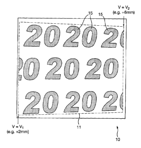
according to the invention. Figure 2 shows the appearance of a first
embodiment of a device 10, in plan view. In the Figure, the solid rectangular
outline represents the perimeter of the device itself. The viewer perceives a
magnified image 15 (sometimes referred to as the "synthetically magnified
image(s)"), here comprising a repeating pattern made up of the number "20 ".
To
the viewer, the magnified image 15 appears tilted relative to the device
plane.
To emphasise this in the drawing, the magnified images are enclosed by a
highly
perspectivised rectangle shown in broken lines (although in practice this will
not
be visible), representing the image plane 11. The longer vertical side of the
rectangle represents that part of the image plane closer to the observer,
whilst
the shorter vertical side corresponds to that part of the image plane further
from
the viewer.
In one example, at the left hand side of the device (as orientated in
Figure 2) the image plane 11 appears 2mm behind the surface plane of the
device, whereas on the right hand side of the device the image plane appears
6mm behind the plane of the device. As will be explained further below, this
is
achieved by designing or fabricating the right hand side of image plane to
exhibit
three times the parallax motion (relative to the surface plane) exhibited by
the
left hand side of the image. In doing so, the illusion is created of being
located
at a distance behind the surface plane three times that of the left hand side.
The
rate of parallax motion determines the absolute image depth.
Figure 3 illustrates in cross-section the overall structure of the device
shown in Figure 2. Thus, the device comprises a transparent, PET or other
polymer layer 20 on the upper surface of which is formed a two-dimensional
array of spherical microlenses 22. The diameters of the microlenses 22 is
typically in the range 1-100 microns, preferably 1-50 microns and even more
preferably 10-30 microns, thus defining pitches in a similar range.
The focal length of the microlenses 22 (as measured from their planar
back surface) is substantially equal to the thickness t of the optical spacer
layer
which in this example comprises the thickness of the substrate 20 but could
optionally include the thickness of a print receptive layer (not shown)
provided on
the opposite surface of the substrate 20 to the microlens array 22. Thus, in
this
example, a focal plane 24 is defined which is substantially co-incident with
the
surface of the substrate 20. On the substrate 20 is printed (or otherwise
formed)
CA 02791160 2012-08-24
WO 2011/107782 PCT/GB2011/050398
12
a microimage array 25, an example of which is depicted in Figure 4. The
microimage array generally comprises an array of the icon, symbol, pattern or
other graphic which it is desired to display with the device, reproduced with
much lower dimensions than will ultimately appear to the viewer.
In order to create the phenomena of moire magnification and enable the
generation of magnified images, a pitch mismatch is introduced between the
microimage array 25 and the microlens array 22. One method for producing
magnification is to have a microlens and microimage array with substantially
the
same pitch where the pitch mismatch is achieved by introducing a small
rotational misalignment between the microimage and microlens array. The
degree of rotational misalignment between the microimage and microlens array
is preferably in the range 15 - 0.06, which results in a magnification range
of
between -4X-1000X for the microimage array. More preferably the rotational
misalignment is in the range 2- 0.10, which results in a magnification range
of
between -25X-500X for the microimage array.
Alternatively, magnification can be produced by the microimage array and
microlens array are in substantially perfect rotational alignment but with a
small
pitch mismatch. A small pitch mismatch would equate to a percentage
increase/decrease of the pitch of the microimage array relative to the
microlens
array in the range 25% - 0.1 %, which results in a magnification range of
between
-4X-1000X for the microimage array. More preferably the percentage
increase/decrease of the pitch of the microimage array relative to the
microlens
array is in the range 4% - 0.2%, which results in a magnification range of
between -25X-500X for the microimage array.
It is also possible to use a combination of a small pitch mismatch and a
small rotational misalignment to create the phenomena of moire magnification
and enable the generation of moving images.
The result of the pitch mismatch between the array 25 and the spherical
lens array 22 causes moire magnification of the microimages. If the pitch
mismatch is constant across the array, the magnified images will appear to the
viewer to be located on a flat image plane which is parallel to the device
surface.
However, in the present embodiment, the pitch mismatch is not constant but
rather is arranged to continuously vary along one axis (here, the x-axis)
across
at least a region of the device (in this example, the variation occurs across
the
CA 02791160 2012-08-24
WO 2011/107782 PCT/GB2011/050398
13
whole device depicted). This can be achieved either by continuously varying
the
pitch of the microlens array 22, or by continuously varying the pitch of the
micro-
image array 25, or both. In the present example, the pitch of the microlens
array
22 is substantially constant, and that of the microimage array 25 is varied as
will
now be demonstrated.
The degree of magnification achieved by moire magnification is defined
by the expressions derived in "The Moire magnifier", M. Hutley, R Hunt, R
Stevens & P Savander, Pure Appl. Opt. 3 (1994) pp.133-142.
To summarise the pertinent parts of this expression, suppose the micro
image pitch = A and the micro lens pitch = B, then magnification M is given
by:
M = A / SORT [(Bcos(Theta) - A)2 - (B sin(Theta))2]
where, Theta equals angle of rotation between the 2 arrays.
For the case where A 0 B and where Theta is very small such that
cos(Theta) = 1 and sin(Theta) = 0:
M = A/ (B-A) = S/(1-S) .. (1)
Where S = B/A
However for large M > > 10 then S must unity and thus
M.=u1/(1-S)
The "depth" of the synthetic image relative to the surface plane derives
from the familiar lens equation relating magnification of an image located a
distance V from the plane of lens of focal length f. This being
M=V/f-1 ...(2)
Or, since typically v/f 1
M=V/f
Thus the depth V of the synthetically magnified image = M* f .
Suppose the structure of Figures 2 and 3 was comprised of micro lenses
22 with a focal length f of 40 pm or 0.04mm. Furthermore let us suppose both
the micro lenses and the supporting substrate 20 where both comprised of
materials with refractive index n of 1.5. Then it follows that the base
diameter D
of the lenses will constrained by the expression
D < f * 2 (n-1) and therefore D < 0.04 *2(1.5-1) giving D s 0.04mm.
CA 02791160 2012-08-24
WO 2011/107782 PCT/GB2011/050398
14
We might then choose a value for D of 0.035mm and a lens pitch B of 0.04mm
(along each of the x and y axes), resulting in a lens array with a f /# number
close to unity with reasonable close packing (inter lens gap 5 urn).
By controlling the pitch of the microimage elements, the magnification
level and depth of the resulting image can be controlled. Considering first,
for
comparison, the case of a flat image plane parallel to the device surface: in
a
first example, suppose we require the image plane to be located 2mm behind
the surface plane of the substrate 20 (note images behind the surface plane
are
by definition "virtual" and a more detailed analysis shows them to be non-
inverted relative to the micro image object array 25).
For further illustrative simplicity we assume in this illustration that the
pitch of the
microimage elements is the same along the x and y axes (i.e. Ay, = Ax,).
Given M = v/ f , then it follows if f = 0.04mm and v= 2mm, then M, = 2/0.04 =
50.
Therefore since M, = A, / (B-A1) = 50, it follows 50 (B - A,) = A,, giving A,
= B
(50/51)
Substituting B = 0.04mm, we obtain A, = 0.0392mm.
In a second example, suppose we wish to obtain a flat image plane 6mm
behind the plane of the device. Now, M2 = 6/ 0.04 = 150 and thus 150 (B-A2) _
A2, giving A2 = B (150/151) = 0.0397mm.
So it can be seen that different image plane "depths" (V) can be achieved
through the use of different microimage array pitches (A).
Therefore, to achieve tilt or curvature of the image plane, the perceived
depth can be made to change between one position on the device and another
by continuously varying the microimage array pitch (A) across the device.
Above, we have denoted the distance or depth of the image plane relative to
the
surface plane by the symbol V (the value of V for a particular image plane
being
constant across the surface of the device). However in the present embodiment,
CA 02791160 2012-08-24
WO 2011/107782 PCT/GB2011/050398
the value of V varies with distance x from the left hand edge of the device.
Therefore, V is a function of x and thus it is pertinent to write that V =
V(x). In
other embodiments, the depth V could additionally or alternatively vary in the
y-
axis direction, so more generally, V= V(x,y),
5 In the present embodiment, as shown in Figure 3, the desired image
plane 11 is flat and titled at an angle to the device surface, with its left-
most side
(x = 0) appearing at a depth V1 = 2mm behind the device surface, and its right-
most side (x : xm) at a depth V2 = 6mm behind the device surface. Taking the
device surface as V = 0, for simplicity, and applying the straight line
equation:
10 V(x) = kx + C ...(3)
where k and C are constants, we can substitute the known values at x = 0 and x
xmax, and, rearranging, write:
(V(x) -2) / x = (6 - 2) / Xmax
Therefore for a particular value of x, the value V(x) can be easily
determined.
Now since the image depth V is a function of x, from equation (2) above,
so therefore is the magnification M and thus the image pitch A (assuming the
lens pitch B is fixed). Therefore, combining equations (1) and (2) we may
write:
A(x) = B * [1 - f /v(x)]
As before if we assume in this embodiment that B = 0.04mm and f = 0.04mm,
then:
A(x=0) = 0.04 [1- 0.04/2] = 0.0392mm
A(x=xmax) = 0.04 [1- 0.04/6] = 0.0397mm
A(x=xmax/2) = 0.04 [ 1-0.04/4] = 0.0396mm
In this way, the pitch A(x) required at each location of the microimage
array 25 along the x-axis in order to produce an image plane 11 of the desired
tilt
can be calculated. The microimage elements can then be printed or otherwise
formed onto the substrate 20 at the calculated positions such that the pitch
variation is incorporated into the array.
Figure 4 shows an example of a suitable microimage element array 25
which may be used to form the device shown in Figures 2 and 3, illustrating a
plurality of microimage elements 26. Each microimage element 26 takes the
form of a numeral "20", which is essentially the same as the "20"'s in the
CA 02791160 2012-08-24
WO 2011/107782 PCT/GB2011/050398
16
magnified image (see Figure 2), but typically several tens or hundreds of
times
smaller in dimension. The microimages could alternatively comprise a set of
s and an adjacent set of "0"'s with a similar result.
At the left-hand side of the array 25, i.e x=O, the pitch A( o) between
adjacent microimage elements 26 (in the x-direction) is selected to return an
image depth V0,=0) of +2mm. At the right-most side of the array 25, i.e. x =
xmax,
the pitch A(xvxmax) between adjacent microimage elements is selected to return
a
greater image depth V(x-xmax) of +6mm. Between x = 0 and x = xmax, the pitch A
continuously varies: in this example, the pitch increases by 0.0005mm from one
side of the array to the other. Preferably, the pitch changes between each
adjacent pair of elements 26 - for instance, the spacing between elements 26a
and 26b in Figure 4 is slightly less than that between elements 26b and 26c.
In
this way, the gradual change in image plane depth will be perceived as a
smooth
surface to the human eye. However, in some cases the same result can be
achieved if two or more adjacent pairs of elements share the same spacing.
As mentioned above, in this example, the pitch variation is only applied
along the x-axis ("A(x)") but in other embodiments the pitch of the microimage
element array could instead vary along the y-axis ("A(y)"), which would result
in
a plane appearing to tilt towards the "top" or "bottom" edge of the device
rather
than the left/right edges. In still further embodiments, the pitch could vary
along
both the x and y axes, in which case the image plane would appear to tilt in
both
directions.
It will be noted that, in Figure 4, the size of the individual microimage
elements 26 also changes from the left to the right of the array 25. This is
not
essential. If all of the microimage elements are formed at the same size,
there
will be distortion of the magnified image for the reasons now discussed. In
some
implementations this can be made use of as a visual effect in itself. However,
in
the present embodiment, it is desired to remove size distortion so that the
magnified elements appear to have substantially the same size as each other.
To understand how the tilted magnified image is generated we first note
that the perceived depth is given by the approximation:
Depth (v) = M x focal length of lens array (f)
where M = synthetic magnification (see equation (1) above).
CA 02791160 2012-08-24
WO 2011/107782 PCT/GB2011/050398
17
It therefore follows that the micro images located at that part of the
synthetic
image 6mm behind the device surface will be magnified by three times the
amount experienced by those micro images located at that part of the image
only 2mm behind the surface plane. Consequently if there is to be no size
distortion of the numeral '20' then it follows that the microimage elements 26
located at the 6mm "deep" area of the image plane must be one third the size
of
those under the 2mm "deep" area of the plane. That is, the height "h" of the
elements 26 varies between h(X_o) and h~x_x,r,,,x) where h(x_0) = 3.h(,
xi1,~ix)'
It should also be realised that all variations in micro image size and pitch
for intermediate depths can be calculated in a similar way and in particular
the
values for the middle of the planar synthetic image will be the mean of the
values
for the 2mm and 6mm "deep" areas of the plane. Thus, for example, h
(x=xmax/2) = [ h (x =0) + h(xmax) ] = [ 3 +1 ]. h(x=xmax) /2 = 2 h(x=xmax).
A second embodiment of a device is depicted in Figures 5 and 6. Here,
the device is formed using the same principles described with respect to the
first
embodiments, but the tilted image plane intersects the plane of the device
surface. That is, referring to Figure 5, the left-hand side of the image plane
11
appears to the viewer to be located above the device, and the right-hand side
of
the image plane 11 appears to be located below the device surface. The
position at which the image plane appears to intersect the device is labelled
V=O.
To illustrate this concept, consider first an example of a flat image plane
parallel to the device surface and located 2mm in front of the device, using
the
same exemplary values for the other parameters as before.
In contrast to the previous examples, here the magnified image of array
25 will be a real inverted image and thus the sign of the magnification will
be
negative (which follows from assigning a negative value for the image depth V
in
the previous expression for magnification).
Hence M=-2/0.04=-50 and thus -50(B-A)=A,giving A=50/49B=
0.0408mm.
Hence we see that for the image plane to be located in front of the
surface plane (i.e appearing to float) the micro image array must have a pitch
larger than the lens pitch. Conversely if the image pitch is less than the
lens
CA 02791160 2012-08-24
WO 2011/107782 PCT/GB2011/050398
18
pitch then the image array will appear to be located below the surface plane
(as
in the previous examples).
Thus the image plane can be positioned in front of the device surface
through control of the pitch mismatch. As such the calculations set out in
relation to
the first embodiment can be applied in the same way (using V(x-o)= V, = -2 and
V. ,,- V, = +4 for example) to determine appropriate pitch variations with
which
the array of micro-images should be formed in order to arrive at the image
surface
shown in Figures 5 and 6. For example, V(x=xmax/2) = (-2+4)12 = 1 mm
A(x=0) = 0.04 [ 1+ 0.04/2] = 0.0408mm
A(x-xmax) = 0.04 [ 1- 0.04/4] = 0.0396mm
A(x=xmax/2) = 0.04 [ 1-0.04/1] = 0.0384mm
Figures 7 and 8 illustrate a third embodiment of a device in which two or
more overlapping image planes are generated in the same region of the device.
This can be particularly advantageous where a multicoloured device is desired,
since each image plane arises from its own respective microimage element
array. As such, the two microimage element arrays can be formed in different
colours since they do not need to be in registration with one another.
However,
this is not essential and the two arrays could be of the same colour if
desired.
Figure 7a illustrates the appearance of the complete device in plan view.
Two sets of magnified images are visible, one overlying the other. A first set
of
magnified images, here "star" symbols 15 appear to lie on a tilted first image
plane 11. This first image plane 11 is shown on its own in Figure 7b. Over the
star symbols, a second set of magnified images 150, here the numeral "5"
appears on a flat second image plane 110, parallel to the device surface (in
Figure 7a, the periphery of second image plane 110 therefore coincides with
that
of the device itself, and is not visible). Figure 7c shows the second image
plane
110 alone. In combination, since one set of images appears to lie "above" the
other, when the device is tilted, there will appear to be relative movement
between the "stars" and the "5"'s.
Thus the first, tilted, image plane 11 is formed using the same principles
as described above with respect to the first and second embodiments. Namely,
a first array of microimage elements 25 is formed on the substrate 20 (see
Figure 8), with the pitch of the elements incorporating a continuous variation
in at
least one axis, as previously described. The second image plane 110 is formed
CA 02791160 2012-08-24
WO 2011/107782 PCT/GB2011/050398
19
by applying a second array of microimage elements 250 to the same surface of
the substrate 20. However, since in this example the second image plane is to
be parallel to the device surface, the pitch of the second microimage element
array 250 is kept constant across the array. In practice, if the first image
plane
11 will be perceived as lying behind the second image plane 110 (as in the
present example), the second microimage element array may be applied to the
substrate before the first microimage element array such that the elements of
the
second microimage element array are not obscured by those of the first. Of
course, the first image plane could alternatively be arranged to appear in
front of
the second, in which case the order of laying down the microimage element
arrays may be reversed.
It will be appreciated that the second image plane 110 could,
alternatively, also be tilted or curved using the same principles applied to
the
generation of the first image plane 11. For example, both planes could be
arranged to appear tilted to the same angle, spaced from but parallel to each
other. Alternatively, the two planes could be tilted at different angles and
could
converge or diverge from one another. The two planes may also intersect one
another and/or the device surface. An example of an intersecting embodiment
will be described below.
Three or more image planes could be provided by providing three or
more corresponding microimage element arrays in a corresponding manner.
As already alluded to, the image surfaces generated using the presently-
disclosed principles need not be planar but could instead be curved. Figure 9
illustrates a fourth embodiment of the invention in which the generated image
surface is curved. Again, this is achieved by varying the pitch of the micro-
image element array 25 (and/or that of the microlens array 22) at least along
the
x-axis. In this case, instead of using the straight line equation (3) as in
the
embodiments above, the desired depth variation V(x) can be defined as a curve.
Examples include curves defined by circular, elliptical, parabolic or other
forms
of polynomial function and those defined by forms of trigonometric function..
In
one particularly effective implementation, the image plane could be configured
to
curve in both the x and y axis, giving the device the appearance of a 3D
spheroidal surface on which the magnified images are presented.
CA 02791160 2012-08-24
WO 2011/107782 PCT/GB2011/050398
Curved image surfaces such as that shown in Figure 9 can be combined
with one or more other flat, tilted or curved image surfaces to achieve a
superposition of image surfaces as described with respect to Figures 7 and 8.
In the above embodiments, the pitch mismatch variation has been applied
5 across one region of the device which generally encompasses the whole
device.
However, additional effects can be achieved by designating different laterally
spaced (but preferably abutting) regions of the device to have different
variations
in the pitch mismatch and hence display different image surfaces to the
viewer.
In one example, the pitch mismatch variation could be restricted to a portion
of
10 the device, such that the image surface only appears tilted or curved in
that
region, and in the surrounding areas it appears flat and parallel to the
device
surface. However, more complex structures can yield interesting effects such
as
that depicted in Figure 10 as a fifth embodiment of the invention. Here, in a
first
region R, of the device, the image plane 11a is configured to tilt away from
the
15 viewer - i.e. the depth V increases with distance x. In a second region R2,
the
image plane 11b is configured to tilt towards the viewer - i.e. the depth V
decreases with distance x. The two regions abut one another at x = x*, and the
image planes 11 a and 11 b are arranged to intersect one another at the same
position. The result is a "chevron" shaped image plane 11 (made up of regions
20 11a and 11b) which appears as a "valley" to the viewer. Of course, the
arrangement of the two regions could be reversed so as to appear as a "hill".
By
arranging for the tilt or curvature to take place along the y-axis direction
as well
as in the x-axis, the complexity of the surface can be further increased.
The present invention is not limited to any specific type or geometry of
microlens, the only requirement being that the microlens can be used to form
an
image. Microlenses suitable for the present invention include those that
refract
light at a suitably curved surface of a homogenous material such as plano-
convex lenslets, double convex lenslets, and fresnel lenses. Preferably the
present invention will comprise spherical microlenses but lenses of any
symmetry including cylindrical lenses could be employed. Both spherical and
aspherical surfaces are applicable to the present invention. It is not
essential for
the microlenses to have a curved surface. Gradient refractive index (GRIN)
lenses image light by a gradual refraction throughout the bulk of the material
as
a result of small variations in refractive index. Microlenses, based on
diffraction,
CA 02791160 2012-08-24
WO 2011/107782 PCT/GB2011/050398
21
such as Fresnel zone plates can also be used. GRIN lenses and amplitude or
mask based fresnel zone plates enable the surface containing the microlens
array to be planar and offers advantage in print receptivity and durability.
It is preferable to use a periodic array of lenses generated by a replication
process. Master microlens arrays can be produced by number of techniques
such as photothermal techniques, melt and reflow of photoresist and
photoresist
sculpture. Such techniques are known to those skilled in the art and are
detailed
in chapter 5 of "Micro-Optics: Elements, Systems, and Applications" edited by
Hans Peter Herzig, published by Taylor and Francis, reprinted 1998. The
master microlens structure can then be physically copied by commercially
available replication techniques such as hot embossing, moulding or casting.
Materials into which the microlens structures can be replicated include but
are
not limited to thermoplastic polymers such as polycarbonate and
polymethylmethacrylate (PMMA) for the hot embossing and moulding processes
and acrylated epoxy materials curable by heat or radiation for the casting
process. In a preferred process the microlens array is replicated via casting
into
a UV curable coating applied to a carrier polymer film such as PET.
For simplicity, the examples and embodiments herein describe the use of
spherical microlenses.
As an alternative, the security device of any of the embodiments could be
fabricated as a mirror-based moire device, of which an example is shown in
Figure 11. In this case, the spherical microlens array 22 is replaced by a
spherical or aspheric concave mirror array 40 formed on one surface of the
transparent polymer substrate 20. The other surface is provided with one or
more microimage element arrays 25, 250 as before. In this particular example,
the microimage elements are printed onto a print receptive layer 23 provided
on
the substrate 20. In each of the embodiments, the microlens array 22 or
concave mirror array 4 can be integrally moulded into the polymer substrate 20
or could be formed on the surface of the substrate 20, for example by cast-
curing or the like.
The ray diagram included in Figure 11 shows how the mirror array 40
reflects ambient light passing through the microimage element array(s) and
presents a magnified version of the underside of the array(s) to the viewer.
The
effect is the same as that perceived using micro-lens based embodiments, and
CA 02791160 2012-08-24
WO 2011/107782 PCT/GB2011/050398
22
the resulting image plane(s) can again lie above or below the device surface.
To
achieve tilting or curvature of the image plane(s), the microimage element
array(s) and/or the mirror array is arranged to vary in pitch along at least
one
axis using the same principles discussed above.
In this example, two microimage element arrays 25, 250 are provided.
The first microimage element array 25 is configured to present to the viewer
an
image plane 11 which is tilted up towards the right hand side of the Figure.
The
second microimage array 250 is configured to present an image plane 110 which
is tiled in the opposite direction and intersects the first image plane 11.
Thus, in
the left portion of the device, the first image plane will appear behind the
second
and this order will be reversed on the right hand side.
In the example shown, the first microimage element array 25 is depicted
as having been applied to the print receptive layer 21 first, then followed by
the
application of the second micro image array 250. This will ensure that the
reflective image pertaining to the first image plane is visualised as being in
front
of the second plane of micro images on the right hand side of the image.
However, on the left hand side of the image the order of laying down the
microimage elements may need to be reversed to avoid confusion in the image.
Since, in this embodiment, the incident light has to pass through or be
transmitted by the printed micro image arrays 25, 250 (i.e. spatially
modulated)
before being reflected back as collimated light by the mirror array, then it
follows
that if the print micro images are substantially opaque the synthetically
magnified
images will take on a blackish colour or hue against the metallic hue provided
by
the mirror background. For the synthetically magnified images to appear with
the colour of their corresponding micro image array then it is necessary that
the
micro images are at least partially translucent. The more translucent the
micro
images the brighter the colour of the synthetic images - however at a cost of
reduced image contrast relative to the background.
If the metal coating on the mirrors is `white' reflector such as Aluminium
then the background hue or colour surrounding the synthetic images will be
silver - white or achromat in appearance. However it should be recognised that
other affordable coloured metals such as Copper or it alloys maybe be used.
Other metals such as Silver, Gold, Platinum, Chrome, Nickel, Nickel-Chrome,
Palladium, Tin etc may be used where there.
CA 02791160 2012-08-24
WO 2011/107782 PCT/GB2011/050398
23
It should be noted that the focal length of a concave mirror is equal to half
its radius of curvature R and therefore can have a limiting minimum value
approaching one quarter of the mirror base diameter. In simple terms, for a
given
base diameter the focal length and F number of a mirror can be one quarter of
the value of equivalent lens (assuming typical refractive index of 1.5).
However
as reducing F number equates to reducing depth of focus, then in practice it
will
often be desirable to have a mirror base diameter much less than 2R.
For example considering the preferred device thicknesses cited earlier
we may require the mirror focal length to be 40um - then this requires the
mirror
radius R to have a value 80um and thus a maximum theoretical base diameter
approaching 160um and thus an F number f/# = 0.25mm. This structure is
intended for viewing only in reflection mode and thus is most relevant for
application onto opaque substrates (strip & patch) or partially embedding into
opaque substrates (windowed thread). As per the lens system the printed micro
images must be coincident with the focal plane of the mirrors to a precision
determined by the depth of focus or field of the mirror system. Other
possibilities for lens-based systems will be discussed below with reference to
Figure 18.
Figure 12a illustrates part of suitable apparatus for printing the micro
image elements onto the substrate 20. The apparatus shown in Figure 12
comprises an inking roll 70 coupled via a roll chain 72 to an ink reservoir
74. Ink
is transferred by the roll 70 onto a print roll 76 carrying proud printing
elements
78 corresponding to the microimage elements of the array concerned. The
substrate 20 is fed between the print roll 56 and an impression roller 80 and
the
image elements are printed onto the substrate 20.
A second apparatus similar to that shown in Figure 12a may be provided
downstream of that apparatus to print a second array of microimage elements if
desired.
Figure 12b illustrates alternative apparatus suitable for printing the image
elements. Ink is transferred by the roll 70 onto a print roll 82 carrying
recessed
printing elements 83 corresponding to the microimage elements of the array
concerned. A doctoring blade 84 contacts and removes ink or colorant off the
non-recessed areas of the print roller 82. The substrate 20 is fed between the
printing roller 82 and an impression roller 80 and the image elements are
printed
CA 02791160 2012-08-24
WO 2011/107782 PCT/GB2011/050398
24
onto the substrate. A second apparatus similar to that shown in Figure 12b may
be provided downstream of that apparatus to print another array of image
elements if desired.
Microlenses or concave micromirrors are provided on the opposite
surface of the substrate 20 by cast-curing, moulding or the like.
In the examples described above, the microimage elements have been
provided by printing onto the substrate. It would also be possible to provide
some or all of the image elements as relief structures and examples of some of
these are shown in Figures 13A-13J. In these Figures, `IM' indicates the parts
of
the relief generating an image while 'NI' indicates those parts which do not
generate an image.
Figure 13A illustrates embossed or recessed image elements. Figure
13B illustrates debossed image elements. Figure 13C illustrates image
elements in the form of grating structures while Figure 13D illustrates moth-
eye
or other fine pitch grating structures.
These structures can be combined. For example, Figure 13E illustrates
image elements formed by gratings in recesses areas while Figure 13F
illustrates gratings on debossed areas.
Figure 13G illustrates the use of a rough embossing.
Figure 13H illustrates the provision of print on an embossed area while
Figure 131 illustrates "Aztec" shaped structures.
Figure 13J illustrates ink filled recesses.
The various embodiments of the device construction described above can
be slit or cut into patches, foils, stripes, strips or threads for
incorporation into
plastic or paper substrates in accordance with known methods.
In one embodiment the current invention could be incorporated into a
security paper as a windowed thread.
In further examples, the security device also includes one or more other
optical security features. An example of this is shown in Figure 14. In this
example, a moire magnifier device 30 is formed as described with reference to
any of the above-described embodiments. The security device also includes a
number of holographic image generating structures 100. The holographic image
structures 100 can be cast or embossed into the same resin as the microlenses
but equally two different resins, one suitable for casting the microlenses and
one
CA 02791160 2012-08-24
WO 2011/107782 PCT/GB2011/050398
suitable for embossing a holographic structure could be applied in register.
Alternatively the holographic structures could be embossed into a polymeric
lacquer positioned on the opposite side of the polymeric layer to the
microlenses.
5 The holographic generating structures 100 can be in the form of
holograms or DOVID image elements. In the label construction shown in Figure
14, the microlenses and the visualisation of the magnified image array(s) is
located in a central horizontal band or region of the label whilst the
holographic
generating structures 100 are located on either side. However, it should be
10 understood that this example is purely illustrative and for example the
holographic generating structures 100 could be located in a central band or
strip
with the moire magnifier 30 being provided in one or more regions on either
side.
Alternatively moire magnified images and the image provided by the holographic
generating structures could be integrated into a single image by each
providing
15 components of a single image. Figure 15 illustrates an example of such an
integrated design where the holographic generating structures 101 form a
scroll
and in the middle of the scroll the holographic structures are replaced with a
moire magnifier 30 to create a moire magnified image in this case of moving
"5"'s and stars (e.g. as described with respect to Figure 7 above).
20 In the case of the holographic structures 100, 101 these can have any
conventional form and can be fully or partially metallised. Alternatively the
reflection enhancing metallised layer can be replaced with a substantially
transparent inorganic high refractive index layer, such as ZnS.
Whatever arrangement is defined, it is advantageous if the individual
25 regions allocated to the two different optical effects in Figures 14 and 15
are
sufficiently large to facilitate clear visualisation of the effects.
The security devices shown in the previous figures are suitable to be
applied as labels to secure documents which will typically require the
application
of a heat or pressure sensitive adhesive to the outer surface of the device
which
will contact the secure document. In addition an optional protective
coating/varnish could be applied to the exposed outer surface of the device.
The
function of the protective coating/varnish is to increase the durability of
the
device during transfer onto the security substrate and in circulation.
CA 02791160 2012-08-24
WO 2011/107782 PCT/GB2011/050398
26
In the case of a transfer element rather than a label the security device is
preferably prefabricated on a carrier substrate and transferred to the
substrate in
a subsequent working step. The security device can be applied to the document
using an adhesive layer. The adhesive layer is applied either to the security
device or the surface of the secure document to which the device is to be
applied. After transfer the carrier strip can be removed leaving the security
device as the exposed layer or alternatively the carrier layer can remain as
part
of the structure acting as an outer protective layer. A suitable method for
transferring security devices based on cast cure devices comprising micro-
optical structures is described in EP1897700,
The security device of the current invention can also be incorporated as a
security strip or thread. Security threads are now present in many of the
world's
currencies as well as vouchers, passports, travellers' cheques and other
documents. In many cases the thread is provided in a partially embedded or
windowed fashion where the thread appears to weave in and out of the paper.
One method for producing paper with so-called windowed threads can be found
in EP0059056. EP0860298 and W003095188 describe different approaches for
the embedding of wider partially exposed threads into a paper substrate. Wide
threads, typically with a width of 2-6mm, are particularly useful as the
additional
exposed area allows for better use of optically variable devices such as the
current invention. The device structures shown in any of the Figures could be
used as a thread by the application of a layer of transparent colourless
adhesive
to one or both of the outer surfaces of the device. Careful selection of the
optical
properties of the adhesive in contact with the microlenses is important. The
adhesive must have a lower refractive index than the microlens material and
the
greater the difference in the refractive index between the microlenses and the
adhesive the shorter the back focal length of the lenses and therefore the
thinner
the final security device.
The security device of the current invention can be made machine
readable by the introduction of detectable materials in any of the layers or
by the
introduction of separate machine-readable layers. Detectable materials that
react to an external stimulus include but are not limited to fluorescent,
phosphorescent, infrared absorbing, thermochromic, photochromic, magnetic,
electrochromic, conductive and piezochromic materials.
CA 02791160 2012-08-24
WO 2011/107782 PCT/GB2011/050398
27
Additional optically variable materials can be included in the security
device such as thin film interference elements, liquid crystal material and
photonic crystal materials. Such materials may be in the form of filmic layers
or
as pigmented materials suitable for application by printing.
The security device of the current invention may comprise an opaque
layer.
Figures 16 and 17 shows a further security feature in the form of a
demetallised image incorporated within a security device of the current
invention.
The magnified image arrays of the device 30 are observed in the central band
of
the device. This provides a primary security effect due to the strong
lenticular
type animation. As can be seen in Figure 17, the structure of the feature
shown
in Figure 16 along section A-A is as shown in Figure 8. In the regions outside
of
the central band exhibiting moire magnification (as seen along section B-B)
the
print receptive layer 21 has been metallised 200. Parts 205 of the metal layer
are demetallised to define the demetallised images thus enabling the creation
of
demetallised indicia which can be viewed in reflective but more preferably
transmitted light.
In a further example and in reference to the mirror-based moire example
shown in Figure 11 the metallised layer forming the micromirrors may be
extended beyond the micormirrors and then parts of this layer can be
demetallised to define demetallised images.
One way to produce partially metallised/demetallised films in which no
metal is present in controlled and clearly defined areas, is to selectively
demetallise regions using a resist and etch technique such as is described in
US-B-4652015. Other techniques for achieving similar effects are for example
aluminium can be vacuum deposited through a mask, or aluminium can be
selectively removed from a composite strip of a plastic carrier and aluminium
using an excimer laser. The metallic regions may be alternatively provided by
printing a metal effect ink having a metallic appearance such as Metalstar
inks
sold by Eckart.
The presence of a metallic layer can be used to conceal the presence of
a machine readable dark magnetic layer. When a magnetic material is
incorporated into the device the magnetic material can be applied in any
design
but common examples include the use of magnetic tramlines or the use of
CA 02791160 2012-08-24
WO 2011/107782 PCT/GB2011/050398
28
magnetic blocks to form a coded structure. Suitable magnetic materials include
iron oxide pigments (Feet3 or Fe304), barium or strontium ferrites, iron,
nickel,
cobalt and alloys of these. In this context the term "alloy" includes
materials
such as Nickel:Cobalt, Iron.Aluminium:Nickel.Cobalt and the like. Flake Nickel
materials can be used; in addition Iron flake materials are suitable. Typical
nickel
flakes have lateral dimensions in the range 5-50 microns and a thickness less
than 2 microns. Typical iron flakes have lateral dimensions in the range 10-30
microns and a thickness less than 2 microns.
In an alternative machine-readable embodiment a transparent magnetic
layer can be incorporated at any position within the device structure.
Suitable
transparent magnetic layers containing a distribution of particles of a
magnetic
material of a size and distributed in a concentration at which the magnetic
layer
remains transparent are described in W003091953 and W003091952.
Figures 18a and 18b show two schematic figures, illustrating how lens
based moire systems would operate in reflection only mode and in both
reflection and transmission respectively. Figure 18a shows the reflection only
scenario where the device 10 having a similar structure to that of Figure 8 is
either applied onto a substantially opaque substrate 31 (e.g. a banknote or
other
security document) or partially embedded into an opaque substrate (e.g. as a
windowed thread) via an adhesive layer 32. In this case the synthetically
magnified image viewed by the observer is ultimately derived from light that
has
been back scattered or reflected from the micro image arrays 25, 250 and the
medium that acts as a background to the micro -image array. The greater the
reflective contrast between the micro image arrays and the surrounding back
ground medium the greater the visual contrast of the synthetically magnified
images. Now it may be that the colour or reflective properties of the
substrate 31
are non optimal - for example the substrate may be of low reflectivity or a
similar
colour to one of the micro image arrays. To address this we show in Figure 18a
the addition of an optional mask coat layer 33 located between the micro print
interface and the adhesive layer 32 bonding to the device to the substrate 31.
The mask layer 33 will typically contain a reflective opacifying pigment such
as,
but not limited to, titanium dioxide particles in a resin binder. The colour
of this
layer could be simply white or a colorant could be added to ensure that this
CA 02791160 2012-08-24
WO 2011/107782 PCT/GB2011/050398
29
mask layer or background reflecting layer exhibits a desired hue which
contrasts
with one or both micro image arrays.
In a further example the mask coat and one of the micro image arrays
have overtly the same color, however one or other entity has been provided
with
a metameric property. Consequently under normal viewing the relevant micro
image array is only weakly discerned (if at all) against the background colour
of
the opaque mask - however when viewed under a metameric filter said micro
image array or more pertinently its synthetically magnified image becomes
strongly evident. Alternatively the mask coat may be provided with a
fluorescent
additive such that when viewed under a fluorescent light the mask coat
provides
a fluorescent background against which the absorbing micro image arrays form
black synthetically magnified images. Examples of metameric inks are provided
in GB1407065. The mask coat may also function as a durability enhancing layer.
Figure 18b shows the scenario where the device 10 is applied at least
partially over a transparent aperture 3 within the substrate 31. It is well
known to
incorporate security devices into transparent apertures within secure
documents
(see below). In this case the synthetically magnified image may be viewed in
reflection and / or transmission through the viewing aperture 3 in the
substrate
31. The observer will only see magnified image when located in position #1. As
can be seen in figure 18b, the opaque mask coat is omitted so we can observe
the moire magnification system in transmission. It is also a requirement that
the
adhesive layer 34 have good optical clarity (i.e. low scatter low absorption)
It should be note that if the printed micro-images 25, 250 are formed from
an ink or colorant that is substantially opaque, then the synthetically
magnified
image will be coloured when viewed in reflection, but will form a high
contrast
essentially black image when viewed in transmission.
A requirement for a coloured image to be viewed in transmission is that
the micro images must have some degree of translucency. Light must be able to
pass through the printed images and the desired colour transmitted.
Note also that if the observer views the device from location #2, then no
synthetically / moire magnified image is observed , but instead an unmodified
or
direct image of the micro image patterns.
The substrate 31 may form part of a security document and may itself be
formed from any conventional material including paper and polymer. Techniques
CA 02791160 2012-08-24
WO 2011/107782 PCT/GB2011/050398
are known in the art for forming transparent regions in each of these types of
substrate. For example, W08300659 describes a polymer banknote formed
from a transparent substrate comprising an opacifying coating on both sides of
the substrate. The opacifying coating is omitted in localised regions on both
5 sides of the substrate to form a transparent region.
EP1141480 describes a method of making a transparent region in a
paper substrate. Other methods for forming transparent regions in paper
substrates are described in EP0723501, EP0724519, EP1398174 and
W003054297.
10 One or more of the disclosed microimage arrays may be printed with inks
comprising materials that respond visibly to invisible radiation. Luminescent
materials are known to those skilled in the art to include materials having
fluorescent or phosphorescent properties. It is also well known to use other
materials that respond visibly to invisible radiation such as photochromic
15 materials and thermochromic materials. For example only one of the
magnified
arrays might be visible in normal daylight conditions with the second
magnified
image becoming visible only under UV illumination. Alternatively the two
magnified arrays could appear the same colour in normal daylight conditions
and
different colours when viewed using a filter or when viewed under UV
20 illumination.