Note: Descriptions are shown in the official language in which they were submitted.
CA 02791293 2012-08-28
WO 2011/124605 PCT/EP2011/055343
- 1 -
Method for the operational control of an inverter
The invention relates to a method for the operational
control of an inverter designed for DC/AC voltage
conversion.
In electrical installations in which a direct voltage
generated by photovoltaic elements is converted into
alternating voltage by means of transformerless
inverters, capacitive leakage currents may occur in
dependence on the circuit and the modulation method
selected, since the potential of the solar generator
can fluctuate with respect to ground potential. This
can influence a residual-current-operated protective
device of the inverter negatively, for example.
One reason for the occurrence of leakage currents is an
alternating-voltage component which, due to the circuit
topology and the modulation of the inverter, is
superimposed on the direct voltage generated by the
photovoltaic elements. The leakage currents drain off
to ground potential (PE) via so-called leakage
capacitances (external ones of the photovoltaic element
and those inside the inverter).
Although it is attempted to reduce this effect by
optimizing the inverter topology, the effect of
capacitive leakage currents can, however, occur in
spite of such an optimization in certain operating
states even in the case of transformerless inverters of
more recent construction, especially in the case of
inverters that are not operated in the conventional
sine-delta-modulation.
Such a transformerless inverter of more recent
construction, especially optimized and advantageous
with regard to its efficiency, in so-called "three-
CA 02791293 2012-08-28
WO 2011/124605 PCT/EP2011/055343
2 -
point topology" is disclosed in EP 2 107 672 A2. It
shows a three-phase transformerless inverter with a
link, the inputs on the direct-voltage side of which
are connected to one another by two series-connected
capacitances, the two capacitances defining a center
voltage point that is not connected to the neutral
conductor of the alternating-voltage grid.
In such a three-point topology, the voltage at the
input UDC to PE is, in case of normal pulse width
modulation (PWM) that is generated in accordance with
the common principle of sine-delta modulation, a direct
voltage so that in this case, in which a link voltage
at the input of the inverter bridge must be at least as
large as twice the peak voltage of the line voltage
signal so that the modulation degree of the PWM is less
than or equal to 1, initially no leakage currents
occur. If the link voltage is reduced to a value below
twice the peak voltage of the line voltage signal, this
results in overmodulation for the PWM, i.e. a
modulation degree of greater than 1, which leads to
distortion for the current at the inverter output.
To achieve as good an efficiency as possible, it is
advantageous to keep the link voltage as low as
possible. For this purpose, methods are known,
especially for three-phase inverters, in which, for
example, in the case of conventional sine-delta
modulation, a time-variant offset, for example a delta
signal with three times the line frequency or a sine
signal with three times the line frequency is added so
that, in spite of the occurrence of link voltage values
below twice the peak voltage of the line voltage signal
in the PWM signal itself, no overmodulation occurs, and
thus also no current distortion of the inverter output
signal fed into a grid occurs. Such modulation methods
include, for example, also the methods known by the
CA 02791293 2012-08-28
WO 2011/124605 PCT/EP2011/055343
3 -
terms "space vector modulation" or "sine-delta
modulation with third harmonic".
In the case of modified sine-delta modulation methods,
especially in the case of the aforementioned methods of
sine-delta modulation with time-variant offset, an
alternating voltage component with three times the line
frequency occurs, for example, but not only, in the
aforementioned transformerless inverter from
EP 2 107 672 A2, due to its topology, between the
voltage center point at the input and PE, which causes
a capacitive alternating current via the leakage
capacitances (leakage current).
Inverters usually have a residual-current-operated
protective device, which detects the differential
currents on the alternating-current side and, in the
case of a fault, e.g., in order to avoid danger to
persons or damage to the inverter itself, switches the
inverter off. However, the differential current
measured contains not only the fault current actually
to be detected but additionally in a vectorial sum also
a leakage current, which may be present, so that
leakage currents that are too large can lead to an
erroneous triggering of the residual-current-operated
protective device and, thus, to an unwanted switching-
off of the inverter. Refraining from the use of
modulation methods in which leakage currents can occur
due to topology will again worsen the efficiency and,
therefore, does not represent a suitable solution to
this problem.
Against this background, the invention has the object
of limiting the disadvantageous effects of leakage
currents on the operation and on the operational
behavior of inverters and at the same time preferably
also ensuring as good an efficiency as possible.
CA 02791293 2012-08-28
WO 2011/124605 PCT/EP2011/055343
4 -
The invention achieves this object by means of the
subject matter of claim 1. A method for the operational
control of an inverter designed for DC/AC voltage
conversion is disclosed, the inverter having at least
one direct-voltage input and being connectable to a
power supply grid via at least one alternating-voltage
output - or two or more alternating-voltage outputs -,
the inverter being involved in a power flow interaction
with the grid, in such a manner that, during operation
of the inverter, a leakage current IA can occur, the
method being characterized by the fact that the leakage
current IA is controlled by the operational control.
Due to the fact that the leakage current or currents is
or are controlled, it is possible to ensure in a simple
manner that predeterminable maximum values for leakage
currents are not exceeded.
In principle, the invention is suitable for different
inverters in which leakage currents, especially
capacitive leakage currents to ground potential, occur
at the input side. In particular, these are
transformerless inverters of different topologies, as
well as topologies in which the neutral conductor (N
potential) of the grid is not connected. The method is
preferably suitable for three-phase inverters which can
have both a two-point topology (e.g. a so-called B6
bridge) and a multi-point topology, for example a
three-point topology (e.g. an NPC "Neutral Point
Connected" bridge or a BSNPC "Bipolar Switch Neutral
Point Connected") bridge.
Especially preferably, the method is used for the
operational control of a transformerless inverter,
particularly in the case of an inverter that does not
have a galvanic connection to or with an N and/or PE
potential of the power supply grid.
CA 02791293 2012-08-28
WO 2011/124605 PCT/EP2011/055343
-
In particular, the invention also provides for an
operation, optimized with regard to the efficiency, of
the inverter in spite of the occurrence of capacitive
leakage currents at the input.
5
In the operational control of the inverter for driving
a power component assembly of the inverter that has
power semiconductors, a PWM method is preferably used
and the actual operational control is done by means of
a control device. In this context, the method is
suitable especially - but not exclusively - for pulse
width modulation types in which a modified sine-delta
modulation, especially with time-variant offset, is
used for generating the PWM signal. In this context, it
is advantageous if the amplitude of the offset is not
constant but is always chosen to be just as large as is
necessary for avoiding overmodulation of the PWM signal
generated. As a result, an offset with zero amplitude,
and, thus, conventional sine-delta modulation, is
obtained for values of the link voltage at or above
twice the peak voltage of the line voltage signal.
Since, in an advantageous embodiment of the method
according to the invention, the link voltage influences
the leakage current, this can be used, in turn, for
implementing a control of the leakage current in a
simple manner. The leakage current IA is thus preferably
controlled by changing a target value setting for the
link voltage UZWK TGT at the input of the inverter bridge.
Thus, control can always take place, for example, when
the link voltage UZWK has a voltage value that is
greater than a predeterminable first voltage limit (Ul)
and when the link voltage UZWK has a voltage value which
is less than a predeterminable second voltage limit
(U2) .
CA 02791293 2012-08-28
WO 2011/124605 PCT/EP2011/055343
6 -
The leakage current IA is preferably controlled when the
inverter is in an operating state in which at least one
certain condition is met. According to a particularly
advantageous embodiment, this condition can consist in
that the inverter is operated within a range in which
the offset of the modulation method has a value unequal
to zero. This is particularly advantageous since the
leakage currents to be controlled occur in certain
inverter topologies only when the inverter is operated
within this range. This range is limited upward by a
link voltage value U2 that corresponds to twice the peak
voltage of the line voltage signal and downward by a
minimum link voltage value Ul up to which an operation
without current distortion in the inverter output
signal is possible with the respective method of sine-
delta modulation with time-variant offset.
The condition can also consist in that the leakage
current IA has a current value that is greater than a
predeterminable first current limit, the leakage
current IA then being controlled to a current value that
is less than or equal to a second predeterminable
current limit.
It is suitable if the following holds for the first
current limit: IA = 0 and the following holds for the
second current limit: IA = IMAX, ImAx being a current
value above which the inverter is transferred into a
safe state by its residual-current-operated protective
device.
It is advantageous if the control of the leakage
current is so slow that it does not respond to rapidly
occurring fault currents, which should trigger the
residual-current-operated protective device, but, at
the same time, is also fast enough, such that occurring
CA 02791293 2012-08-28
WO 2011/124605 PCT/EP2011/055343
7 -
leakage currents are controlled before the residual-
current-operated protective device responds to them.
It is further advantageous if the inverter has a DC/DC
converter (preferably a boost converter or a buck
converter or a combined buck-boost converter) at the
input so that in the operational control, apart from
controlling the leakage current, maximum power point
tracking can also be performed for maximizing a power
delivered by the photovoltaic elements without these
two control systems having a disadvantageous effect on
one another.
Further advantageous embodiments of the invention are
specified in the remaining subclaims.
In the text which follows, the invention will be
described in greater detail by means of exemplary
embodiments, with reference to the drawings, in which:
Figure 1 shows a basic block diagram of a system
with an inverter connected between a PV
generator and a power grid;
Figure 2 shows a basic block diagram of a system
analogous to figure 1, with an inverter
that has a three-point topology;
Figures 3a, b show diagrams for illustrating the
variation in time for the link
potential and for the alternating
output voltage with respect to M* and
with respect to PE when the inverter is
driven by sine-delta modulation with
delta-shaped offset;
Figures 3c, d show diagrams for illustrating the
variation in time for the link
potential and for the alternating
output voltage with respect to M* and
CA 02791293 2012-08-28
WO 2011/124605 PCT/EP2011/055343
8 -
with respect to PE when the inverter is
driven by sine-delta modulation with
sinusoidal offset;
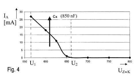
Figure 4 shows a diagram that shows the
variation of the (effective) leakage
current over the link voltage;
Figures 5, 7 show flowcharts for illustrating two
possible embodiments of the method for
controlling the leakage current;
Figure 6 shows an U/I characteristic for
controlling the leakage current;
Figure 8 shows a basic block diagram of a system
analogous to figure 1, with an inverter
that has a three-point topology and a
DC/DC converter at the input.
In the following text, figures 1 and 2 are used for
initially describing the configuration of a PV system
as well as an exemplary, highly simplified
transformerless inverter topology.
In an electrical installation of the type of figure 1,
a photovoltaic generator (PV generator) 1 consisting of
at least one photovoltaic element generates a direct
voltage that is supplied to the direct-voltage inputs
of an inverter 4 via electrical lines 2 and 3. The
direct voltage supplied to the inverter is converted by
the inverter into an alternating voltage and fed into a
power supply grid (represented by the components on the
right of line 5) at outputs 10, 11, 12.
A capacitance CX 6 represents the so-called equivalent
leakage capacitance, i.e., the sum of all leakage
capacitances via which leakage currents may flow. The
alternating-voltage components of a voltage UX between a
ground potential (PE) and the electrical line 3 cause
the leakage currents flowing via the capacitance CX 6.
CA 02791293 2012-08-28
WO 2011/124605 PCT/EP2011/055343
9 -
The voltage thus represents a measure of the leakage
current IA flowing. As an alternative or additionally,
the voltage between the electrical conductor 2 and the
ground potential (PE) can also be used as a measure of
a leakage current.
The inverter 4 has component assemblies not shown in
detail here, such as a power component assembly with
power semiconductors and a control device (with a
driving assembly) and possibly further assemblies such
as filters, a user interface, various interfaces,
measuring devices, etc.
Figure 2 shows a PV system with an inverter in "three-
point topology". An exemplary embodiment of such an
inverter is described in greater detail, for example,
in EP 2 107 672 A2.
The capacitances Cl and C2 shown additionally are used
for dividing the direct voltage generated by the PV
generator and for forming three voltage levels.
Furthermore, figure 2 shows a line filter with the
components LNl, LN2, LN3, CNl, CN2 and CN3, the bottom end
of which is connected to the connection between the two
capacitances Cl, C2 and the center voltage input of the
inverter. This connection is designated by the circuit
point M*. The voltage UM between the circuit point M*
and the ground potential (PE) represents a measure of
the leakage current IA. The N-conductor (not shown in
figure 2) of the alternating voltage grid may be
connected to the inverter in order to be used as
reference potential for measuring purposes,
particularly also as a reference for the residual-
current-operated protective device. However, it is not
conductively connected to the actual assemblies of the
CA 02791293 2012-08-28
WO 2011/124605 PCT/EP2011/055343
- 10 -
inverter that are used for voltage conversion, thus,
the potential of M* is free with respect to PE/N.
The inverter bridge 7 contains the bridge circuit
consisting of power-electronic switches (for example an
NPC bridge or a BSNPC bridge) for converting direct
current at the input into alternating current at the
output.
The inverter is driven/controlled by means of pulse
width modulation that is preferably generated by means
of sine-delta modulation with time-variant offset.
Figures 3a and b show, for example, the case of sine-
delta modulation with delta-shaped offset, also known
as "space vector modulation", figures 3c and d show the
case of sine-delta modulation with sinusoidal offset,
also known as "sine-delta modulation with third
harmonic". In addition, other forms of modified sine-
delta modulation are also possible, especially such
with other shapes of the offset, which allow a direct-
voltage signal with a value of less than twice the peak
voltage of the line voltage signal to be converted into
an inverter output signal that does not exhibit any
current distortions. It is advantageous if the
amplitude of the offset is not constant but is always
chosen to be of just such a magnitude as is necessary
such that for a given link voltage no current
distortions are obtained.
Figure 3 shows in each case the superimposed three line
voltage variations L1, L2 and L3 and the variations of
the positive (ZwK+) and negative (ZwK-) link potential
with respect to the M* potential (fig. 3b and 3d) and
with respect to the ground potential PE (fig. 3a and
3c). In this context, it can be seen that the positive
and negative potentials of the link circuit always
envelop the three line voltage variations.
CA 02791293 2012-08-28
WO 2011/124605 PCT/EP2011/055343
- 11 -
If the inverter is operated in sine-delta modulation
with time-variant offset, the link voltage UZWK = (ZwK+)
- (ZwK-) can , thus, drop below the value U2 shown in
fig. 3a, b and 3c, d (i.e., twice the value of the peak
voltage U of the line voltage signal) . In this case,
however, there will be fluctuations of the potential at
the input with respect to the ground potential PE.
These fluctuations, which have three times the line
frequency, cause leakage currents (see fig. 4).
Although, in principle, in the case of sine-delta
modulation with time-variant offset the link voltage
can be lower than twice the value of the peak voltage U
of the line voltage signal, it may only be of a
magnitude such that the link potential variation always
envelops the line voltage variations, i.e., the link
potential may not be lower than the value Ul as can be
seen in fig. 3a. Thus, the following holds for
operation within the range of modulation with offset:
Ul < UZWK < U2.
Figure 4 shows exemplarily the dependence of a leakage
current IA on the link voltage UZWK (cf. the voltage
between conductors 2 and 3 in fig. 2) with a leakage
capacitance of CX = 850 nF. The arrow pointing upward
illustrates the increase in leakage current IA with
increasing leakage capacitance C>.
During the operation of an inverter of the type
mentioned, limits exist for the leakage current IA.
Thus, the leakage current must not rise above a maximum
value IN,AX, above which a disconnection from the power
grid is done by the residual-current-operated
protective device.
CA 02791293 2012-08-28
WO 2011/124605 PCT/EP2011/055343
- 12 -
On the other hand, the requirement to operate inverters
with the highest possible efficiency demands for the
link voltage UZWK to be reduced below the value U2 which,
in turn, results in a leakage current IA (compare
fig. 4).
It has hitherto been proposed to limit the permissible
leakage capacitances to a maximum value so that leakage
currents occurring do not exceed a particular value.
However, this has the result that certain photovoltaic
elements having leakage capacitances that are too high
cannot be used in combination with certain inverter
topologies. It has also been proposed to deactivate the
operation with link voltages below twice the peak
voltage of the line voltage signal when leakage
currents occur that are too high, which, however, leads
to a reduction of the efficiency, which may eventually
happen also temporarily. Both of these options are
disadvantageous.
Also, the leakage capacitances are not constant in time
but can fluctuate, e.g., due to condensation, humidity
or other influences. PV systems, therefore, have always
had to be dimensioned up to now on the basis of the
worst conditions in order to prevent frequent
switching-off due to leakage currents that were too
high.
In order to achieve the optimum operational control of
the inverter, as possible, taking into consideration
the limitations described, it is therefore proposed to
control the leakage current IA in such a manner that the
leakage current IA does not exceed a maximum value IMAx
while still operation with the highest possible
efficiency is achieved by keeping the link voltage as
low as possible by using suitable modulation, for
example sine-delta modulation with time-variant offset,
CA 02791293 2012-08-28
WO 2011/124605 PCT/EP2011/055343
- 13 -
and continuous control, with the leakage current acting
as control quality criterion.
For this purpose, the link voltage UZWK is reduced, for
example, by changing the target value setting UZWK TGT for
the link voltage control as long as the leakage current
IA does not exceed a particular maximum value I.
If the leakage current IA threatens to exceed the
maximum value IN,AX, the link voltage UZWK is increased by
increasing the target value setting UZWK TGT, which leads
to a reduction of the leakage current IA. During this,
the PWM signal is always adapted by the modulation
method used, such that for the respective link voltage
at the input of the inverter no current distortions
occur in the signal at the inverter output.
Figure 4 also shows two voltage values UT and U2 for the
link voltage UZWK. UT designates the value of the link
voltage UZWK that is, for example with sine-delta
modulation with time-variant offset, required at
minimum for generating the line voltage amplitudes to
be fed in. U2 designates the value of the link voltage
below which the inverter would be operated in
overmodulation (modulation index M>1) with conventional
sine-delta modulation.
The values UT and U2 are dependent on the type of
modulation and also on the line voltage. They are
determined by a central processing unit, or specified
by it, respectively.
In the text that follows, the exemplary flowchart shown
in fig. 5 is described.
CA 02791293 2012-08-28
WO 2011/124605 PCT/EP2011/055343
- 14 -
At first, in step 100, the target value setting for the
link voltage UZWKTGT is set to a starting value above or
equal to U2-
In step 101, the actual value of the leakage current IA
is measured.
With the measurement value IA, a voltage difference AU
is determined in step 102 by using the characteristic
AU = f(IA) shown exemplarily and schematically in
figure 6. The larger the amount of the leakage current
IA measured, the larger the voltage difference AU is.
The steepness of the characteristic shown in figure 6
specifies the amount by which AU is changed when the
measured leakage current IA changes by a particular
amount (applies to: Il < IA < 12, cf. fig. 6) .
In step 103, a new lower limit value U4 is formed from
the lower limit value U1, which is predetermined by the
modulation method, by adding the voltage difference AU
already determined. The upper limit U3 for the voltage
difference AU, given in the characteristic according to
fig. 6, ensures, due to the U3 >_ U2-U1 relationship,
that the new lower limit value U4 is not increased
further after the upper voltage limit U2 is reached or
exceeded, since there is no further voltage dependence
of the leakage current IA on the link voltage UZWK via U2
according to fig. 4 and, thus, an increase in the link
voltage UZWK cannot cause any further reduction in the
leakage current IA. Such a situation can occur, for
example, when a base leakage current is present that is
greater than the current value I2. As can be seen in
conjunction with fig. 6, U1 is retained as lower limit
below the current value I 1 r i . e . U4=U1, since AU = 0.
By means of the evaluation shown in step 104, it is
determined whether the actual target value setting for
CA 02791293 2012-08-28
WO 2011/124605 PCT/EP2011/055343
- 15 -
the link voltage UZWK TGT is greater than the lower
voltage limit U4. If this is the case("yes branch"), the
current target value setting for the link voltage UZWK TGT
is reduced in accordance with the exemplary calculation
rule given in step 105. In this step, the dynamic range
and the absolute value of this adaptation are
influenced by a control parameter k3, which is
advantageous to be less than one and greater than zero
for this calculation rule. Subsequently, the leakage
current IA is measured again and the lower voltage limit
value U4 is adapted again, beginning with step 101.
If the condition in step 104 is not met ("no branch"),
i.e., if the actual target value setting for the link
voltage UZWK TGT is below the lower voltage limit U4 or at
this limit, the target value setting for the link
voltage UZWRTGT is increased in accordance with the
exemplary calculation rule given in step 106. In this
step, the dynamic range and the absolute value of this
adaptation are influenced by a control parameter k4,
which is advantageous to be less than or equal to one
and greater than zero for this calculation rule.
Subsequently, the leakage current IA is measured again
and the lower voltage limit value U4 is adapted again,
by passing through the loop and beginning with step
101.
Instead of the exemplary calculation rules 105 and 106,
respectively, any other filtering functions that are
appropriate in the field of control engineering can
also be used. Also for the characteristic AU = f(IA)
other realizations than the one given in figure 6 are
possible.
Furthermore, the control parameters k3 and k4 do not
need to be constant but can be changed adaptively, for
example during the operation.
CA 02791293 2012-08-28
WO 2011/124605 PCT/EP2011/055343
- 16 -
Figure 7 shows exemplarily a further possibility for
implementing the method according to the invention
without the characteristic shown in figure 6.
At first, in step 200, the target value setting for the
link voltage UZWRTGT is set to a starting value above or
equal to U2.
In step 201, the actual value of the leakage current IA
is measured.
If the measured value of IA is below the limit ImAX, the
process branches to step 203 ("yes branch") in the
branching-step 202 and the target value setting for the
link voltage UZWRTGT is reduced in accordance with the
exemplary calculation rule in step 203. The dynamic
range and the absolute value of this adaptation are
influenced here by a control parameter kT which is
advantageous to be greater than zero for this
calculation rule. Subsequently, the leakage current IA
is measured again, beginning with step 201, and checked
for exceeding of I.
If the condition at the branching-step 202 is not met
("no branch"), i.e., if the leakage current IA has
reached or exceeded the value ImAX, the target value
setting for the link voltage UZWK TGT is increased by
means of the exemplary calculation rule specified in
step 205. The dynamic range and the absolute value of
this adaptation are influenced here by a control
parameter k2 which is advantageous to be greater than
zero for this calculation rule. Subsequently, the
leakage current IA is measured again and checked for
exceeding of IMAx by passing through the loop beginning
with step 201.
CA 02791293 2012-08-28
WO 2011/124605 PCT/EP2011/055343
- 17 -
In step 204, an additional check is done as to whether
the actual target value setting for the link voltage
UZWK TGT is below the upper voltage limit value U2, and,
if not, the increase in target value setting for the
link voltage UzWx TGT is bypassed in step 205. This
prevents the target value setting for the link voltage
UzWx SET TGT from being raised above the voltage limit U2,
above which, according to figure 4, there is no further
voltage dependence of the leakage current IA on the link
voltage UZWK. An increase in the link voltage UzWx
therefore cannot produce any further reduction in the
leakage current IA. Such a situation may occur, for
example, if a base leakage current is present that is
greater than IMAX =
Instead of the exemplary calculation rules 203 and 205,
respectively, any other filtering functions that are
appropriate in the field of control engineering can
also be used. As well, the control parameters kT and k2
do not need to be constant but can be changed
adaptively, for example during the operation.
According to the previous explanations, the link
voltage at the input of the inverter bridge is set by
the method according to the invention to the lowest
possible value that is optimal for operation in view of
efficiency. In this manner, the invention, in
particular, allows inverters to be operated with the
lowest possible link voltage at the input of the
inverter bridge in order to optimize their efficiency
although leakage currents can occur in such a type of
operation. This is done by keeping these leakage
currents below a maximum value, that is not to be
exceeded, by means of a control process.
In an arrangement according to figure 2, the link
voltage UZWK at the input of the inverter bridge 7 is,
CA 02791293 2012-08-28
WO 2011/124605 PCT/EP2011/055343
- 18 -
at the same time, also the voltage UDC at the PV
generator 1. In this context, when using the method
according to the invention, it has to be taken into
consideration that, in the case of PV installations,
there is usually a further requirement for the
generator voltage UDC that results from the so-called
"MPP Tracking". Such methods, which, by setting a
particular generator voltage, ensure that the PV
generator operates at the point of maximum power
delivery (Maximum Power Point, MPP), are known to the
one skilled in the art and, therefore, do not need any
further explanations in detail here.
If then the generator voltage UDC required by MPP
Tracking is higher than the target value for the link
voltage UZWK TGT, as determined by the method according to
the invention, the generator voltage required by MPP
Tracking is preferred to be set in the method according
to the invention. If, however, the generator voltage UDC
required by MPP Tracking is less than or equal to the
target value for the link voltage UZWK TGT, as
predetermined by the method according to the invention,
then the voltage value UZWK TGT, as determined by the
method according to the invention, is set in view of
the leakage current IA to be limited. This value is then
usually no longer identical to the voltage value at
which the PV generator is operated at the point of
maximum power delivery. It has to be taken into
consideration also that operating the arrangement
according to figure 2 is no longer possible when
generator voltages are below U.
In order to extend the input voltage range of an
inverter 4, it is known to connect an additional DC/DC
converter upstream of the inverter bridge 7. Figure 8
shows exemplarily a schematic representation of such a
system according to figure 1 which, compared to the
CA 02791293 2012-08-28
WO 2011/124605 PCT/EP2011/055343
- 19 -
embodiment in figure 2, is supplemented by a DC/DC
converter 9 in the direct voltage path of the PV
generator. The DC/DC converter 9 can be constructed as
boost or buck converter or also as combined buck-boost
converter. When using certain DC/DC converters 9,
especially those that do not have any galvanic
isolation between input and output, leakage currents
occur in an arrangement according to figure 8 in the
same manner as in an arrangement according to figure 2.
As a result of this the method according to the
invention can also be used in an arrangement according
to figure 8.
When using, for example, a boost converter as DC/DC
converter 9 in an arrangement according to figure 8, it
is possible, in contrast to an arrangement according to
figure 2, to operate the system also at generator
voltages UDC which, when conventional sine-delta
modulation is used, can be below U2 and, when modified
sine-delta modulation is used, for example sine-delta
modulation with time-variant offset, can be below U. In
conjunction with the method according to the invention,
the arrangement according to figure 8 also proves to be
particularly advantageous, since now both voltage
values can be set to their optimum independently of one
another in the case when the generator voltage UDC
required by MPP Tracking is less than or equal to the
target value for the link voltage UZWK TGT as determined
by the method according to the invention. In this
manner, it is possible to control the leakage current
together with maximum power point tracking without
these two control methods influencing one another in a
disadvantageous way. In the case when the generator
voltage UDC required by MPP Tracking is higher than the
target value for the link voltage UZWK TGT as determined
by the method according to the invention, the generator
voltage required by MPP Tracking is also set preferably
CA 02791293 2012-08-28
WO 2011/124605 PCT/EP2011/055343
- 20 -
in the method according to the invention in an
arrangement according to figure 8 with boost converter
as DC/DC converter.
Overview of the formula and reference symbols used
1 PV generator
2,3 Lines
4 Inverter
5 Line
6 Capacitance CX
7 Inverter bridge
9 DC/DC converter
10, 11, 12 Outputs
AU [V] Increase of the voltage limit Ul
C1, C2 [nF] Voltage divider capacitances
CNl, CN2, CN3 [nF] Line filter capacitances
CX [nF] Equivalent leakage capacitance
Il [mA] Leakage current limit above which
the lower limit of the link voltage
is increased
12 [mA] Leakage current limit up to which
the lower limit of the link voltage
is increased
IA [mA] Leakage current
IMAX [mA] Maximum permissible leakage current
kl Control parameter
k2 Control parameter
k3 Control parameter
k4 Control parameter
LNl, LN2, LN3 [mH] Line filter inductances
M [-] Modulation Index
M* Circuit point
PE Ground potential
PV Photovoltaics
CA 02791293 2012-08-28
WO 2011/124605 PCT/EP2011/055343
- 21 -
[V] Peak value of the line voltage
signal
UT [V] Lower limit of the link voltage UZWK
below which the line voltage
variations can no longer be
generated
U2 [V] Limit of the link voltage UZWK below
which the inverter is operated in
sine-delta modulation with time-
variant offset
U3 [V] Maximum value for the increase AU
U4 [V] Lower limit of the link voltage UZWK
which is produced by increasing UT by
Au
UDC [V] Voltage at the PV generator
UM [V] Voltage between M* and PE
UX [V] Voltage between PE and line 3
UZWK [V] Link voltage
UZWK TGT [V] Target value setting for the link
voltage
ZwK - Negative link potential
ZwK + Positive link potential