Note: Descriptions are shown in the official language in which they were submitted.
CA 02791674 2012-10-03
UNIVERSAL INTEGRATED CIRCUIT CARD APPARATUS AND
RELATED METHODS
FIELD OF DISCLOSURE
[0001] The present disclosure relates to universal integrated circuit cards,
including but not limited to, universal integrated circuit card apparatus and
related
methods.
BACKGROUND
[0002] Electronic devices, including portable electronic devices, have gained
widespread use and may provide a variety of functions including, for example,
telephonic, electronic messaging, and other personal information manager (PIM)
application functions. Portable electronic devices include, for example,
several
types of mobile stations such as simple cellular telephones, smart telephones,
tablet computers, wireless personal digital assistants (PDAs), and laptop
computers with wireless 802.11 or Bluetooth capabilities.
[0003] Electronic devices such as, for example, portable electronic devices
often
connect to a network (e.g., a mobile network). These devices often employ a
Universal Integrated Circuit Card (hereinafter UICC) to identify a subscriber
for
network access. For example, the UICC can store a Subscriber Identity Module
(e.g., a SIM card, USIM card, RUIM, CSIM, etc.) that authenticates a
subscriber to
a network such as a mobile network. The UICC may also store other subscriber-
related information for non-telecom applications. For example, the UICC can
enable contactless data flow for identity, security, banking, payment
applications
and/or any other application associated with transmitting and securing
personal
data of a user.
BRIEF DESCRIPTION OF THE DRAWINGS
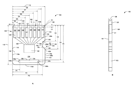
[0004] FIG. 1A illustrates an example UICC disclosed herein.
[0005] FIG. 1B is a side view of the example UICC of FIG. 1A.
1
CA 02791674 2012-10-03
,
,
[0006] FIG. 2A illustrates the example UICC of FIG. 1A and FIG. 1B being
inserted in a first example input device in a first orientation.
[0007] FIG. 2B illustrates the example UICC of FIG. 1A and FIG. 1B being
inserted in a second example input device in the first orientation.
[0008] FIG. 3A illustrates the example UICC of FIG. 1A and FIG. 1B being
inserted in a third example input device in a second orientation.
[0009] FIG. 3B illustrates the example UICC of FIG. 1A and FIG. 1B being
inserted in a fourth example input device in the second orientation.
[0010] FIG. 4A is another example UICC disclosed herein.
[0011] FIG. 4B is a side view of the example UICC of FIG. 4A.
[0012] FIG. 5 is another example UICC disclosed herein.
[0013] FIG. 6A illustrates another example UICC disclosed herein.
[0014] FIG. 6B is a side view of the example UICC of FIG. 6A.
[0015] FIG. 7 illustrates another example UICC disclosed herein.
[0016] FIG. 8 illustrates another example UICC disclosed herein.
,
[0017] FIG. 9A is a perspective view of another example UICC disclosed herein.
[0018] FIG. 9B is a plan view of the example UICC of FIG. 9A.
[0019] FIG. 9C is an exploded view of the example UICC of FIG. 9A and FIG.
9B.
[0020] FIG. 10A is a perspective view of another example UICC disclosed
herein.
[0021] FIG. 10B is a plan view of the example UICC of FIG. 10A.
[0022] FIG. 11 illustrates another example UICC disclosed herein.
2
CA 02791674 2012-10-03
[0023] FIG. 12 illustrates another example UICC disclosed herein.
DETAILED DESCRIPTION
[0024] Universal integrated circuit cards (UICCs) are often used as a
Subscriber
Identity Module (e.g., SIM card, USIM card, RUIM card or CSIM card) in a
portable
electronic device such as a mobile device. A Subscriber Identity Module is a
network access application that is stored in the UICC to authenticate a
subscriber
to a network. In some examples, a UICC enables contactless communication
(Near Field Communication) with a host (e.g., a remote terminal) based on
proximity of the UICC relative to the host.
[0025] Typically, a UICC includes a body to support an integrated circuit or
microprocessor and a plurality of electrical contacts to enable communication
between the microprocessor and a host (e.g., a computer, a mobile device, a
non-
mobile device, a remote terminal, etc.). The host typically employs an input
device (e.g., a card reader) to accept the body and complete a circuit with
the
electrical contacts to enable communication (e.g., transfer data) between the
UICC and the host.
[0026] Currently, physical characteristics or parameters of UICCs are governed
by certain international standards provided by, for example, the European
Telecommunications Standards Institute (ETSI) and the International Standard
Organization (ISO). In particular, physical characteristics or parameters of
an
UICC are provided by certain form factor standards (e.g., ID-1, plug-in UICC,
a
mini-UICC) defined by International Standard Organization ISO/IEC 7816-2 and
7816-3 and/or Technical Specification of the European Telecommunications
Standards Institute ETSI TS 102 221.
[0027] For example, ISO/IEC 7816-2 and/or ETSI TS 102 221 standards define
an overall dimensional envelope of conforming UICCs. For example, mini-UICC
form factor standards define an overall dimensional envelope of a UICC as 15
millimeters by 12 millimeters, which provides a surface area of 180
millimeters
squared. Further, the current standards define a layout of electrical contacts
on
3
CA 02791674 2012-10-03
the UICC as a grid pattern (e.g., 4 by 2 grid pattern) that provides a surface
area
greater than 1 centimeter squared.
[0028] Further, an order or arrangement in which electrical contacts are to be
positioned on the UICC is also defined by the standards. For example, the
standards specify that a first row of electrical contacts should include a
voltage
supply, a reset, a clock and an optional first auxiliary, and a second row of
electrical contacts should include a ground, a single-wire protocol, an
input/output
and an optional second auxiliary. However, by providing such an arrangement,
the first row of electrical contacts typically pass across electrical contacts
of an
input device associated with the second row of electrical contacts when the
UICC
is inserted into the input device, which may cause the circuit card to become
electrically damaged (e.g., short circuit). Further, the supply voltage (e.g.,
the
first contact in the first row) is disposed adjacent the ground (e.g., the
first
contact in the second row), which may increase and/or cause a greater amount
of
electromagnetic interference (EMI).
[0029] While the current specifications ISO/IEC 7816-2 and 7816-3 and ETSI IS
102 221 define standards of a UICC, such standards also influence the design
(e.g., the size, shape or footprint) of an input device or card reader, which
can
also significantly increase a dimensional envelope of a portable electronic
device.
In some example electronic devices, an input device or card reader covers the
greatest amount of surface area of an electronic board of an electronic device
(e.g., a mobile phone) compared to other electronic components of the
electronic
device. For example, by specifying the electrical contacts or pads disposed
across
an (x) by (y) surface area, an input device having a minimum surface area
specified by the (x) by (y) surface area of the electrical contacts is
required to
properly couple to the electrical contacts of the circuit card. However,
smaller
electronic devices are generally desirable for portability. As a result,
current
standards may not be sufficient to reduce the size and/or an overall footprint
of a
mobile device.
4
CA 02791674 2012-10-03
[0030] Some known input devices often employ a push-push mechanism to
insert/remove a UICC from an input device. A push-push mechanism requires a
user to slide the card inside a slot of the input device. To remove the card,
a user
pushes the card further into the slot and a spring-loaded mechanism ejects the
= card from the slot. However, push-push card readers often require a door
or
other holding element to prevent the UICC from sliding out of the card reader
(e.g., prevent unintended removal of the card). However, the door and/or
holding
element may damage easily and/or are relatively more expensive to manufacture.
[0031] Another example input device or card reader employs a push-pull
configuration. In such example, a UICC is pulled from a slot of the card
reader.
However, UICCs typically have relatively flat and/or smooth surfaces that make
it
difficult for the user to grip and pull the card from the card reader. As a
result,
some example electronic devices employ a tray-style input device or card
reader.
However, tray-style card-readers typically increase the overall costs and
dimensional envelope of an electronic device and/or require a unique tool
(e.g., a
pin) to remove the tray-style card reader from an electronic device.
[0032] In general, example UICCs disclosed herein modify or deviate from the
standards provided by ISO/IEC 7816-2 and 7816-3 and/or ETSI TS 102 221 to
define another UICC form factor standard. In particular, UICCs disclosed
herein
provide significantly smaller overall footprints compared to UICCs
manufactured
per the current specifications and/or standards provided by ISO/IEC 7816-2 and
7816-3 and/or ETSI TS 102 221. In addition, the UICCs disclosed herein also
reduce the overall space requirements of an input device or card reader
coupled to
an electronic device.
[0033] In one example, the overall dimensional envelope of the UICC disclosed
herein may have a height of between about 10.9 and 11.1 millimeters and a
width
of between approximately 8.9 and 9.1 millimeters. As a result, a UICC
disclosed
herein may have a surface area of approximately 99 millimeters squared,
thereby
significantly reducing the overall dimensional footprint or size of a UICC
compared
to known UICCs.
CA 02791674 2012-10-03
= [0034] In another example, a layout scheme of electrical contacts or
electrical
pads may differ from a layout provided by, for example, the current ISO/IEC
7816-2 and 7816-3 and/or the ETSI TS 102 221 standards. For example, the
electrical contacts disclosed herein may be disposed or coupled to the UICC in
a
= single-row orientation or configuration. As a result, an electronic
device may
employ a header-style input device or card reader, which uses significantly
less
surface area of a circuit board (e.g., a logic board) of the electronic device
compared to, for example, a multi-dimensional input device (e.g., a multi-row
card reader).
[0035] Further, unlike known UICC having multi-dimensional electrical
contacts,
aligning the electrical contacts in a single-row configuration makes the UICC
less
prone to electrical damage (e.g., short circuit) that may otherwise occur when
the
circuit card is inserted into an input device as noted above. Additionally or
alternatively, in contrast to the current standards provided by ISO/IEC 7816-2
and
7816-3 and/or ETSI TS 102 221, a supply voltage contact and a ground contact
of
the UICC disclosed herein can be spaced apart from each other to significantly
reduce electrical damage (e.g., short circuit) and/or EMI.
[0036] Additionally or alternatively, example UICCs disclosed herein may
employ a locking mechanism to retain the circuit card in the input device
without
the use of doors. The locking feature also substantially prevents improper
orientation of the circuit card relative to the input device and substantially
prevents movement of the circuit card relative to the input device when an
electronic device experiences sudden shock or vibration (e.g., if the
electronic
device is dropped). Also, to facilitate insertion of the circuit card relative
to the
input device, example UICCs disclosed herein may employ a lead-in feature
(e.g.,
a chamfer). Further, to facilitate removal of the circuit card relative to the
input
device, example UICCs disclosed herein may employ a pick-out feature (e.g., a
ridge, an opening, etc.).
[0037] FIG. 1A illustrates an example UICC 100 disclosed herein (hereinafter
referred to as "UICC"). FIG. 1B is a side view of the example UICC 100 of FIG.
6
CA 02791674 2012-10-03
1A. Referring to FIGS. 1A and 1B, the UICC 100 comprises a body 102 defining a
first or front side 104 and a second or rear side 106 opposite the first side
104.
The first and second sides 104 and 106 of the illustrated example are spaced
apart by a thickness 108 (FIG. 1B). In this example, the thickness 108 is
between
= approximately 0.69 and 0.81 millimeters. Further, in the illustrated
example, a
height 110 of the body 102 may be between approximately 10.9 millimeters and
11.1 millimeters and a width 112 of the body 102 may be between approximately
8.9 millimeters and 9.1 millimeters. In particular, the height 110 of the body
102
is approximately 11 millimeters and the width 112 of the body 102 is
approximately 9 millimeters.
[0038] As shown in FIG. 1A, the body 102 of the illustrated example includes a
generally rectangular shape defining a first surface 114. More specifically,
the first
surface 114 has a surface area of approximately 99 millimeters squared. As
shown
in the illustrated example of FIG. 1A, the first surface 114 of the body 102
is
defined by peripheral edges 116. In particular, the first surface 114 is
defined by
a first edge 118a (e.g., a left edge), a second edge 118b (e.g., an upper
edge), a
third edge 118c (e.g., a right edge), and a fourth edge 118d (e.g., a bottom
edge). The second edge 118b is positioned opposite the fourth edge 118d
relative
to the body 102 and the first edge 118a is positioned opposite the third edge
118c
relative to the body 102. The second and fourth edges 118b and 118d are
disposed between the first and third edges 118a and 118c, and the second and
fourth edges 118b and 118d are substantially perpendicular to the first and
third
edges 118a and 118c. As shown, the first and third edges 118a and 118c are
substantially parallel relative to each other and the second and fourth edges
118b
and 118d are substantially parallel relative to each other.
[0039] As shown in FIGS. 1A and 1B, to facilitate insertion of the UICC 100 in
an input device or terminal (e.g., a card reader), each of the peripheral
edges 116
may include a lead-in feature 120. As shown in FIGS. 1A and 1B, the lead-in
feature 120 includes rounded corners each having a radius R1. For example, the
radius R1 of the illustrated example may be less than or equal to 0.80
millimeters.
7
CA 02791674 2012-10-03
[0040] To communicate with a host, the UICC 100 includes an integrated circuit
122 (e.g., an IC). For example, the UICC 100 may include a microprocessor to
communicate with a host via, for example, an input device or terminal. To
communicatively couple the integrated circuit 122 of the UICC to an electronic
= device, the UICC of the illustrated example includes a plurality of
electrical
contacts or contact areas 124. The electrical contacts 124 are disposed on the
first surface 114 adjacent the second edge 118b and between the first and
third
edges 118a and 118c. More specifically, in this example, the electrical
contacts
124 are substantially aligned relative to each other in a single row
orientation or
configuration 126.
[0041] In this manner, an electronic device may employ an input device such
as, for example, a header-style card reader having a significantly smaller
dimensional envelope to significantly reduce an overall dimensional footprint
of
the electronic device. Additionally or alternatively, providing the electrical
contacts 124 in the single row orientation 126 prevents the electrical
contacts 124
from passing over other electrical connectors of an input device as the UICC
100 is
inserted into the input device, which significantly prevents electrical damage
to
the UICC 100. However, in other examples, the plurality of electrical contacts
124
may be disposed on the first surface 114 in a staggered pattern, an offset
pattern,
and/or any other suitable pattern(s). For example, as described below, example
UICC apparatus disclosed herein may include multiple rows of electrical
contacts
124. In some examples, the electrical contacts 124 may be disposed about a
perimeter of the UICC 100 relative to the peripheral edges 116 in, for
example, a
square pattern, a rectangular pattern, etc.
[0042] As shown in FIG. 1A, a classification of the electrical contacts 124
are in
accordance with the classification of electrical contacts provided by
standards
ISO/IEC 7816-2 and 7816-3 and/or ETSI TS 102 221. For example, the electrical
contacts 124 of the illustrated example include a supply voltage contact Cl, a
reset contact C2, a clock contact C3, a first auxiliary contact C4, a ground
contact
C5, a single-wire protocol contact C6 (e.g., (SWP) for Near-Field
Communication
(NFC) or proximity transactions), an input/output contact C7, and a second
8
CA 02791674 2012-10-03
auxiliary contact C8. In some examples, the electrical contacts C4 and C8 can
implement a high speed USB interface between the UICC and the host or
terminal.
The single-wire protocol contact C6 and/or the first and second auxiliary
contacts
C4 and C8 are optional and may be omitted. In other examples, the UICC 100
may employ any other type of electrical contacts other than those described or
represented by electrical contacts C1-C8.
[0043] As shown in FIG. 1A, the plurality of contacts 124 are electrically
coupled
to the integrated circuit 122 via a plurality of wires, traces and/or a bus
128. The
integrated circuit 122 may provide a central processor unit (CPU), volatile
memory
(RAM), non-volatile memory (ROM), etc. The supply voltage contact Cl supplies
the integrated circuit 122 with electricity, the ground contact C5 grounds the
integrated circuit 122, the reset contact C2 resets the integrated circuit
122, the
clock contact C3 provides a clock signal or time reference, and the
input/output
contact C7 enables performance of data input and output. The optional single-
wire protocol contact C6 enables contactless or wireless communication with a
remote terminal or host in proximity with the UICC 100. The optional auxiliary
contacts C4 and C8 enable the UICC 100 to be coupled to, for example,
Universal
Serial Bus (USB) interfaces.
[0044] In addition to the single row orientation 126 to reduce the overall
footprint of an input device and/or significantly reduce the likelihood of
electrical
damage to the UICC 100, the electrical contacts 124 are arranged on the first
surface 114 in a certain order to significantly reduce EMI. For example, the
ground contact C5 is spaced apart from the supply voltage contact Cl. In other
words, at least one other electrical contact C2-C4 and/or C6-C8 (or other
electrical
contacts) is disposed between the ground contact C5 and the supply voltage
contact Cl. As shown in FIG. 1A, the ground contact C5 is disposed adjacent
the
first edge 118a and the supply voltage contact Cl is disposed adjacent the
third
edge 118c. More specifically, in the illustrated example, the ground contact
C5 is
spaced from the supply voltage contact Cl by a maximum distance. Further, the
clock contact C3, which has the highest frequency, is disposed adjacent the
ground contact C5. In this manner, separating the supply voltage contact Cl
and
9
CA 02791674 2012-10-03
the ground contact C5 and/or positioning the clock contact C3 adjacent the
ground
contact C5 significantly reduces EMI.
[0045] Further, in the illustrated example, the second auxiliary contact C8 is
positioned adjacent the clock contact C3, the input/output contact C7 is
positioned
adjacent the second auxiliary contact C8, the single wire protocol contact C6
is
positioned adjacent the second auxiliary contact C8, the first auxiliary
contact C4
is positioned adjacent the single-wire protocol contact C6, and the reset
contact
C2 is positioned adjacent the first auxiliary contact C4. Additionally or
alternatively, the positions of each of the electrical contacts C1-C8 comply
and/or
are within the specification or standards provided by ISO/IEC 7816-2 and 7816-
3
and/or the ETSI TS 102 221. For example, the following table illustrates the
distance of the respective electronic contacts relative to the first edge 118a
as
shown in FIG. 1A.
Electrical Contact Electrical Contact Distance from First
Pin Assignment Edge 118a Value (Millimeters)
C5 Ground D1 0.3
C3 Clock D2 1.4
C8 Second Auxiliary D3 2.5
C6 Single-Wire Protocol D4 3.6
C7 Input/Output D5 4.7
C4 First Auxiliary D6 5.8
C2 Reset D7 6.9
Cl Supply Voltage D8 8.0
[0046] For example, the ground contact C5 is positioned at a distance D1 of
approximately 0.3 millimeters from the first edge 118a, the clock contact C3
is
positioned at a distance D2 of approximately 1.4 millimeters from first edge
118a,
the second auxiliary contact C8 is positioned at a distance D3 of
approximately 2.5
millimeters from the first edge 118a, the single-wire protocol contact C6 is
CA 02791674 2012-10-03
positioned at a distance D4 of approximately 3.6 millimeters from the first
edge
118a, the input/output contact C7 is positioned at a distance D5 of
approximately
4.7 millimeters from the first edge 118a, the first auxiliary contact C4 is
positioned
at a distance D6 of approximately 5.8 millimeters from the first edge 118a,
the
reset contact C2 is positioned at a distance D7 of approximately 6.9
millimeters
from the first edge 118a, and the supply voltage contact Cl is positioned at a
distance D8 of approximately 8.0 millimeters from the first edge 118a.
[0047] Each of the electrical contacts 124 of the illustrated example has a
rectangular shape. As shown in FIG. 1A, each of the electrical contacts 124
has a
width W1 and a height Hl. In this example, the width W1 is approximately 0.7
millimeters and the height H1 is approximately 3.0 millimeters. However, in
other
examples, each of the electrical contacts 124 may have a different sized
height
H1, width W1 and/or may have a square shape, rounded corners and/or any other
suitable shape or configuration or any combination thereof. In addition, the
electrical contacts 124 are equally spaced apart by a distance W2. In the
illustrated example, the distance W2 is approximately 0.40 millimeters.
Further,
both the ground contact C5 and the supply voltage contact Cl are spaced from
the
respective first and third edges 118a and 118c by a distance of approximately
0.3
millimeters.
[0048] Although not shown, in other examples, the electrical contacts 124
illustrated in FIG. 1A can be disposed in any order. For example, the
electrical
contacts 124 may be disposed sequentially C1-C8 and/or in any other suitable
order. In some examples, the first auxiliary input C4 may be disposed adjacent
the first edge 118a of the body 102 instead of the ground contact C5 and/or
the
second auxiliary input C8 may be disposed adjacent the third edge 118c. In
this
example, the overall width 112 of the UICC 100 can be further reduced in
examples in which the auxiliary contacts C4 and C8 are omitted. Additionally
or
alternatively, the electrical contacts 124 may include different contacts
other than
the electrical contacts associated with the classifications C1-C8 as described
in
FIG. 1A. Further, in some examples, any one of the electrical contacts C1-C8
may
be omitted or replaced with another electrical contact.
11
CA 02791674 2012-10-03
[0049] To prevent a metal housing portion of an input device from electrically
damaging (e.g., shorting) the electrical contacts 124 when the UICC 100 is
inserted into the input device, the example UICC 100 includes a buffer area
130
between the second edge 118b and an upper edge 132 of each of the electrical
contacts 124. In other words, the electrical contacts 124 are offset relative
to the
second edge 118b by an offset distance V1. For example, the offset distance V1
may be between approximately 0.1 millimeters and 0.50 millimeters. Further, in
this example, the rounded corners of the body 102 help maintain a
substantially
consistent or relatively even buffer area 130 adjacent the corners of the body
102.
[0050] To facilitate handling and/or insertion/removal of the UICC 100 from an
input device or card reader, the UICC 100 of the illustrated example employs a
grip or pick-out feature 134. In this example, the pick-out feature 134 is
disposed
adjacent the fourth edge 118d between the first and third edges 118a and 118c.
As shown in FIG. 1A, the pick-out feature 134 is a slot or opening. The slot
shown
in FIG. 1A is defined by a rectangular portion 136 disposed between first and
second arcuate or circular ends 136a and 136b. A first portion of the
rectangular
portion is positioned at a distance V4 relative to the second edge 118b and a
second portion of the rectangular portion 136 is positioned at a distance V5
from
the second edge 118b. In this example, the distance V4 may be between
approximately 9.69 and 9.71 millimeters and the distance V5 may be between
approximately 10.39 and 10.41 millimeters such that the slot defines an
opening
sized between approximately 0.68 and 0.72 millimeters. In other examples, the
pick-out feature 134 may be omitted.
[0051] Additionally, a first center 138a of the first arcuate end 136a is
positioned at a distance P1 from the first edge 118a and a second center 138b
of
the second arcuate end 136b is positioned at a distance P2 from the first edge
118a. In the illustrated example, the first distance P1 is between
approximately
1.9 and 2.1 millimeters and the second distance P2 is between approximately
6.9
and 7.1 millimeters from the first edge 118a. In other examples, the pick-out
feature 134 may be a slot having an opening that is recessed in the first
surface
114. In other words, a slot forms a recessed opening that does not pass
through
12
CA 02791674 2012-10-03
the entire thickness 108 of the body 102. In other examples, the pick-out
feature
134 may be a raised lip portion, an aperture and/or any other surface or
feature
to enable or facilitate handling the UICC 100.
[0052] To secure the UICC 100 in a cavity of an input device, the example UICC
100 includes a notch or locking feature 140. More specifically, the notch 140
retains the UICC 100 within an input device and prevents the UICC from moving
(e.g., bouncing) or dislodging from the input device when, for example, the
electronic device experiences a sudden shock (e.g., the device is dropped).
Additionally or alternatively, the notch 140 significantly reduces or prevents
misalignment and facilitates proper orientation of the UICC 100 relative to
the
input device when the UICC 100 is coupled to the input device as described in
greater detail below in connection with FIG. 3A.
[0053] The notch 140 of the illustrated example is disposed along the third
edge
118c of the body 102. In particular, the notch 140 forms a recessed edge 142
spaced away from the third edge 118c and toward the first edge 118a. As shown
in the example of FIG. 1A, the recessed edge 142 is positioned at a distance
of P3
relative to the first edge 118a. In this example, the distance P3 is between
approximately 8.29 and 8.31 millimeters. The notch 140 of the illustrated
example forms a recessed opening 144 having a shoulder or catch feature 146
between a first portion 148a of the third edge 118c and a first end 142a of
the
recessed edge 142 and a substantially tapered edge 150 between a second
portion
148b of the third edge 118c and a second end 142b of the recessed edge 142.
The shoulder 146 is substantially parallel relative to the second edge 118b
and
substantially perpendicular relative to the first portion 148a of the third
edge
118c.
[0054] Additionally, the shoulder 146 is positioned at a distance V2 from the
second edge 118b of the body 102. In this example, the distance V2 is between
approximately 4.49 and 4.51 millimeters. Also, the tapered edge 150 intersects
the second portion 148b of the third edge 118c at a position V3 relative to
the
second edge 118b of the body 102. In this example, the distance V3 is between
13
CA 02791674 2012-10-03
approximately 6.68 and 6.7 millimeters. Further, the example body 102 includes
a radius R2 between the shoulder 146 and the recessed edge 142 and a radius R3
between the tapered edge 150 and the recessed edge 142. In this example, the
radius R2 is less than or equal to 0.3 millimeters and the radius R3 is less
than or
equal to 0.7 millimeters. In other examples, the notch 140 may be omitted. In
other examples, the notch 140 may have any other shape or profile such as
described in FIGS. 11 and 12.
[0055] The example UICC 100 of FIGS. 1A and 1B may be formed via, for
example, a punch-out flat sheet manufacturing process(es). The body 102 may
be composed of, for example, a plastic material and the pick-out feature 134
and/or the notch 140 are formed via, for example, a punching process(es). The
electrical contacts 124 may comprise a unitary sheet composed of electrically
conductive material (e.g., copper, etc.) having divided contacts C1-C8 that
may
be coupled to the first surface 114 of the body 102 via, for example, glue,
solder,
or any other suitable fastener(s). The integrated circuit 122 may be
positioned or
coupled to the body via, for example, a pick and place robot or other
manufacturing equipment. For example, the integrated circuit may be soldered
onto the first surface 114 of the body 102. The wires or traces 128 may be
coupled to the body 102 via wire bonding manufacturing techniques or
process(es).
[0056] Alternatively, as described in greater detail below, the body 102 of
the
example UICC 100 may be composed of a plastic material formed via, for
example, injection molding. In this manner, the body 102 and/or the UICC 100
can be manufactured with more precise tolerances (e.g., relatively tighter
tolerances) compared to the flat sheet manufacturing process as described
above.
For example, the UICC 100 can be manufactured such that the dimensions D1-D8,
P1-P3, V1-V5, R1-R3, H1, W1, W2, the height 110 and/or the width 112 can be
within a tolerance value of approximately 0.1 millimeters.
[0057] FIG. 2A illustrates the example UICC 100 of FIGS. 1A and 1B being
inserted in an example input device or card reader 200 in a first orientation
202.
14
CA 02791674 2012-10-03
Generally, the input device 200 enables communication between the UICC 100
and a host such as, for example, a computer, a point of sale terminal, a
remote
terminal, a mobile device, etc. In addition, the input device 200 provides
power
to the UICC 100 or the integrated circuit 122 and also performs protocol
conversation and/or reformats data for use by the UICC 100.
[0058] In particular, the UICC 100 is inserted in an opening or cavity 204 of
the
input device 200 with a leading edge 206 (e.g., the second edge 118b) of the
body 102 oriented in a direction represented by arrow 208. Further, due to the
single row configuration 126 of the electrical contacts 124, the electrical
contacts
124 do not pass over or across other electrical contacts or connectors of the
input
device 200 when the UICC 100 is inserted in the opening 204. Additionally or
alternatively, the supply voltage contact Cl is adjacent the third edge 118c
and
electrically couples to the input device 200 only when the UICC 100 is fully
inserted in the opening 204. In other words, the electrical contacts 124
simultaneously engage their respective electrical contacts (e.g., not shown)
of the
input device 200 when the UICC 100 is inserted in the input device 200. Thus,
the
UICC 100 receives power only after the UICC 100 is fully inserted and properly
oriented relative to the opening 204 of the input device 200. Such a
configuration
prevents electrical damage to the electrical contacts 124, the UICC 100 and/or
the
input device 200. In addition, placement of the clock electrical contact C3,
which
has the highest frequency, adjacent the ground electrical contact C5
significantly
reduces EMI.
[0059] Further, when the UICC 100 is inserted into the input device 200, the
notch 140 can engage a lock or catch feature 210 of the input device 200 to
secure the UICC 100 in the opening 204 of the input device 200. As a result,
the
UICC 100 remains secured within the input device 200. To remove the UICC 100
from the input device 100, the UICC 100 is moved in the direction of arrow 208
when the UICC 100 is in the opening 204 such that the tapered surface 150
releases the lock or catch feature 210 from the shoulder 142 of the notch 140
(e.g., the tapered surface 150 biases the catch feature 210 away from the
notch
140). A spring-loaded ejection mechanism (not shown) can then eject the UICC
CA 02791674 2012-10-03
100 from the opening 204 and the pick-out feature 134 enables a user to firmly
grasp the UICC 100 and pull it away from the opening 204 in a direction
opposite
of the direction indicated by the arrow 208.
[0060] Further, providing the height 110 with a dimensional value that is
different than the dimensional value of the width 112 significantly prevents
erroneous insertion into the opening 204 of the input device 200.
[0061] FIG. 2B illustrates the example UICC 100 of FIGS. 1A and 1B being
inserted in another example input device or card reader 201 in the first
orientation
202. In contrast with the input device 200 of FIG. 2A, the example input
device
201 of FIG. 2B does not include the locking feature 210 as shown in FIG. 2A.
Nonetheless, the UICC 100 properly fits within an opening 205 of the input
device
201.
[0062] FIG. 3A illustrates the example UICC 100 of FIGS. 1A and 1B being
inserted in another example input device or card reader 300 in a second
orientation 302. Unlike the example of FIG. 2A, the UICC 100 shown in FIG. 3A
is
inserted in an opening 304 of the input device 300 with the third edge 118c of
the
body 102 as a leading edge 306 oriented in a direction represented by arrow
308.
As noted above, the orientation of the electrical contacts 124 as shown in
FIGS.
1A and 1B prevent electrical damage when the UICC 100 is inserted into the
input
device 300. Further, in this example, because the supply voltage contact Cl is
adjacent the third edge 118c or the leading edge 306, the supply voltage
contact
Cl is the last electrical contact 124 to couple to a respective electrical
contact or
connector (not shown) of the input device 300 and does not drag the other
electrical contacts 124 across power. As a result, the UICC 100 is not powered
during insertion of the UICC 100 into the input device 300, thereby
significantly
reducing potential short circuits and/or electrical damage to the UICC 100.
The
UICC 100 receives power only after the UICC 100 is fully inserted into the
opening
204 of the input device 300.
[0063] Additionally or alternatively, the notch 140 as shown in FIG. 3A
facilitates or enables proper orientation of the UICC 100 relative to the
opening
16
CA 02791674 2012-10-03
304 of the input device 300. More specifically, when the UICC 100 is properly
oriented relative the input device 300, a guide feature 310 (e.g., a
protrusion) of
the input device 300 nests within the recessed opening 144 formed or defined
by
the notch 140. In this manner, the UICC 100 can only be properly inserted
within
the opening 304 of the input device 300 when the leading edge 306 of the UICC
100 is inserted within the opening 304 and the second edge 118b of the UICC
100
is adjacent a first side 312 of the input device 300. For example, the UICC
100
may not properly fit within the opening 304 if the second edge 118b is
adjacent a
second side 314 of the input device 300 even if the leading edge 306 is
properly
oriented relative to the opening 304 due to interference between the guide
feature
310 and the edge 118c adjacent the notch 140. Likewise, if the UICC 300 is
inserted in the input device 300 with the first edge 118a as the leading edge,
the
guide feature 310 interferes with the first edge 118a to prevent the UICC 300
from properly fitting within the opening 304. In some examples, the UICC 100
properly fits within the opening 304 when the first edge 118a of the UICC 100
substantially aligns with an end 316 of the opening 304 and/or the input
device
300. For example, improper orientation may cause the first edge 118a of the
UICC 100 to project away from the opening 304 relative to the end 316.
[0064] FIG. 3B illustrates the example UICC 100 of FIGS. 1A and 1B being
inserted in another example input device or card reader 301 in the second
orientation 302. In contrast with the input device 300 of FIG. 3A, the example
input device 301 of FIG. 3B does not include the guide feature 310 shown in
FIG.
3A. Nonetheless, the UICC 100 properly fits within an opening 303 of the input
device 301.
[0065] FIG. 4A is a plan view of another example UICC 400 disclosed herein.
The example UICC 400 of FIG. 4A includes a body 402 defining a first side or
surface 404 and a second surface or surface 406 opposite the first surface
404.
The first and second surfaces 404 and 406 of the illustrated example are
spaced
apart to define a body thickness 408. To facilitate insertion of the UICC 400
into
an input device or card reader, the example UICC 400 of FIG. 4A employs a lead-
in feature 410. As shown in FIG. 4A, the lead-in feature 410 is disposed on a
17
CA 02791674 2012-10-03
leading end 412 of the UICC 400. Additionally, in the illustrated example,
each of
the first and second surfaces 404 and 406 includes the lead-in feature 410.
However, in other examples, only the first surface 404 or the second surface
406
includes the lead-in feature 410. As most clearly shown in FIG. 4B, the lead-
in
feature 410 of the illustrated example includes tapered edges 414a and 414b
adjacent the leading edge 412. In other examples the lead-in feature 410 may
be
chamfered edges, angled edges, rounded edges, or any other shaped-edge to
facilitate insertion of the UICC 400 in an input device such as the input
device 200
of FIG. 2. The lead-in feature 410 may be formed via secondary manufacturing
process(es) such as, for example, machining (e.g., chamfer milling) and/or
other
suitable manufacturing process(es). In some examples, the lead-in feature 410
may be formed via injection molding to eliminate a secondary manufacturing
process as described in greater detail below in connection with FIG. 9A, FIG.
9B
and FIG. 9C.
[0066] FIG. 5 illustrates another example UICC 500 disclosed herein. The UICC
500 of FIG. 5 is implemented with a plurality of electrical contacts 502
(e.g., six
electrical contacts). In the illustrated example, the electrical contacts 502
may
include, for example, the ground contact C5, the clock contact C3, the single-
wire
protocol contact C6, the input/output contact C7, the reset contact C2 and the
supply voltage contact Cl. For example, the first and second auxiliary
electrical
contacts C4 and C8 of FIGS. 1A and 1B may be omitted. In other examples, the
UICC 500 may include only one of the auxiliary electrical contacts C4 or C8 of
FIG.
1A.
[0067] FIG. 6A illustrates another example UICC 600 disclosed herein. FIG. 6B
is a side view of another example UICC 600 disclosed herein. Referring to
FIGS.
6A and 6B, the UICC 600 of FIG. 6A and FIG. 6B is a dual-sided UICC. The UICC
600 of FIG. 6A includes a body 602 defining a first side or surface 604 (FIG.
6B)
and a second side or surface 606 opposite the first surface 604. In
particular, the
first surface 604 of the UICC 600 includes one or more electrical contacts 608
and
the second surface 606 of the UICC 600 includes one or more electrical
contacts
610. For example, the electrical contacts 608 disposed on the first surface
604 of
18
CA 02791674 2012-10-03
the UICC 600 may include the electrical contacts C1-C3, C5-C7 as shown, for
example, in FIG. 5, and the electrical contacts 610 disposed on the second
surface
606 may include, for example, the first and second auxiliary contacts C4 and
C8 of
FIG. 1A. A dual-sided header-style input device or card reader may be employed
to communicatively couple the electrical contacts on both surfaces 604 and 606
of
the UICC 600 to a host (e.g., an electrical device).
[0068] FIG. 7 illustrates another example UICC 700 disclosed herein. As shown
in FIG. 7, the UICC 700 includes a body 702 defining a first side or surface
704
that includes a plurality of electrical contacts 706. In particular, as shown
in FIG.
7, an electrical contact 708 of the plurality of electrical contacts 706 has a
different size and/or shape than the other ones of the electrical contacts
710.
More specifically, the electrical contact 708 expands or covers a greater
surface
area 712 of the first surface 704 relative to the other electrical contacts
710. For
example, as shown, the electrical contact 708 may be a ground electrical
contact
C5. Increasing a surface area of the ground electrical contact C5 may
significantly
reduce EMI.
[0069] FIG. 8 illustrates another example UICC 800 disclosed herein. More
specifically, the UICC 800 of FIG. 8 illustrates another example electrical
contact
configuration 802 expanding across a surface area 804 of a first side or
surface
806 of a body 808 of the UICC 800. As shown, the UICC 800 includes a first
plurality of electrical contacts 810 and a second plurality of electrical
contacts 812.
In particular, the first plurality of electrical contacts 810 are
interconnected or
electrically coupled via a coupling portion 814 to cover a greater amount of
the
surface area 804 of the first surface 806 than for example the electrical
contacts
810 or the electrical contacts 124 of FIG. 1A. For example, the first
plurality of
electrical contacts 810 and the coupling portion 814 may be the ground
electrical
contact C5. As noted above, configuring the ground contact C5 to cover or
expand across a greater amount of surface area on the first surface 806 may
significantly reduce EMI. In other examples, an electrical contact and/or the
coupling portion 814 may span across substantially the entire surface area 804
of
the first surface 806 between peripheral edges 816a-d of the UICC 800.
19
CA 02791674 2012-10-03
[0070] FIG. 9A illustrates a perspective view of another example UICC 900
disclosed herein. FIG. 9B is a plan view of the example UICC 900 of FIG. 9B.
FIG.
9C is an exploded view of the example UICC 900 of FIGS. 9B and 9C.
= [0071] The UICC 900 of FIGS. 9A-9C includes a body 902 defining a first
side or
surface 904 and a second side or surface 906 opposite the first surface 904.
In the
illustrated example, the body 902 or the first surface 904 is approximately 9
millimeters by 11 millimeters and defines a surface area 904a of approximately
99
millimeters squared. The body 902 of the illustrated example is composed of a
plastic material (e.g., a Laser Direct Structuring (LDS) resin) and is formed
via, for
example, injection molding. As shown, because the body 902 may be formed via
injection molding, the example body 902 may include a recessed cavity 912 to
receive an integrated circuit or microprocessor 914. Also, forming the body
902
via, for example, injection molding enables the body 902 to be formed with
relatively more precise and/or tighter tolerances compared to other
manufacturing
process(es) such as, the flat sheet manufacturing process(es) described above.
In
addition, forming the body 902 via injection molding provides a relatively
smoother surface finish to the first surface 904 and/or the second surface 906
and
provides relatively smoother corners 908a-d or edges 910a-d compared to other
manufacturing process(es) such as the flat-sheet manufacturing process.
Providing relatively smoother surface finishes, corners and/or edges
facilitates
insertion and/or an interaction between the UICC 900 and an input device or
card
reader.
[0072] In the illustrated example, after the body 902 is formed via an
injection
molding process, one or more electrical contacts 916 and/or one or more
electrical
traces or connectors 918 electrically coupling the electrical contacts 916 to
the
integrated circuit 914 may be formed or etched in the body 902 via, for
example,
LDS manufacturing process. Such a process enables injection molded plastic
parts
to be selectively plated with discrete circuit pathways (i.e., the traces
918). To
this end, a laser basically etches, writes or prints a conductive pattern
corresponding to the position of the electrical contacts 916 and/or the
electrical
connectors 918 onto the first surface 904 of the body 902 after the body 902
is
CA 02791674 2012-10-03
formed via injection molding. The body 902 is then immersed within a copper
bath to provide the conductive electrical contacts 916 and/or traces 918. For
example, the electrical contacts 916 may include the electrical contacts C1-C8
described in FIG. 1A and may include the electrical contact orientation or
layout
provided by the example UICC 100 of FIG. 1A.
[0073] The integrated circuit or microprocessor 914 may then be disposed in
the cavity 912 of the body 902 via, for example, a pick and place robot and
the
integrated circuit or microprocessor 914 may be coupled to the body 902 via,
for
example, soldering. A cover or screen 920 such as a laminate cover may be
coupled to the body 902 and disposed over the integrated circuit 914 to
protect
the integrated circuit from debris and/or other contaminates.
[0074] To facilitate insertion in an input device, the example UICC 900 of the
illustrated example includes a lead-in feature 922 adjacent a leading edge
924. In
this example, the lead-in feature 922 may be the rounded corners 908b and 908c
and/or may include an arcuate or curved shaped profile. In other examples, the
lead-in feature 922 may be a tapered or chamfered edge adjacent the leading
edge 924 such as, for example, the tapered or chamfered edge 410 illustrated
in
FIG. 4A. The lead-in feature 922 may be formed during the injection molding
process. Thus, unlike the flat-sheet punch out manufacturing process, the
example lead-in feature 922 may be formed with the body 902, thereby
eliminating secondary manufacturing process(es) and/or significantly reducing
costs.
[0075] The example UICC of FIGS. 9A-9C also includes a pick-out feature 926
to facilitate removal of the UICC 900 from an input device. In the illustrated
example, the pick-out feature 926 comprises a raised lip or molded ridge 928
protruding away from the first surface 904 adjacent the edge 910d of the first
surface 904. As shown in FIGS. 9A-9C, the raised lip 928 has an arcuate
profile,
edge or shape. In other examples, the second surface 906 opposite the first
surface 904 may also include a raised lip or molded ridge (e.g., similar to
the
raised lip 928) protruding away from the second surface 906. In some examples,
21
CA 02791674 2012-10-03
the raised lip or molded ridge 928 may be disposed on the second surface 906
instead of the first surface 904.
[0076] The body 902 of the illustrated example also includes a notch 930. The
notch 930 is formed on the edge 910c of the body 902 between the electrical
contacts 916 and the raised lip 928 and provides a catch or locking feature
similar
to the locking feature described in connection with FIGS. 1A and 18.
[0077] FIG. 10A is a perspective view of another example UICC 1000 disclosed
herein. FIG. 10B is a plan view of the example UICC 1000 of FIG. 10A.
Referring
to FIGS. 10A and 10B, the UICC 1000 comprises a body 1002 defining a first or
front surface or side 1004 and a second or rear surface or side 1006 opposite
the
first surface 1004. The body 1002 of the illustrated example includes a
plurality of
electrical contacts 1008 positioned or arranged in a plurality of rows 1008a
and
1008b. For example, a first row 1008a of electrical contacts 1008 may include
the
supply voltage contact Cl adjacent a first edge 1010, the reset contact C2
adjacent the supply voltage contact Cl, the clock contact C3 adjacent the
reset
contact C2, and the first auxiliary contact C4 adjacent the clock contact C3
and/or
a second edge 1012. Additionally, a second row 1008b of electrical contacts
1008
may include the ground contact C5 adjacent the first edge 1010 and below the
supply voltage contact Cl, the single-wire protocol contact C6 adjacent the
ground
contact C5, the input/output contact C7 adjacent the single-wire protocol
contact
C6, and the second auxiliary contact C8 adjacent the input/output contact C7.
[0078] In the illustrated example, the supply voltage contact Cl and the
ground
contact C5 may be disposed a distance of approximately 0.45 millimeters from
the
first edge 1010, the reset contact C2 and the single-wire protocol electrical
contact
C6 may be disposed a distance of approximately 2.65 millimeters from the first
edge 1010, the clock contact C3 and the input/output contact C7 may be
disposed
a distance of approximately 4.85 millimeters from the first edge 1010, and the
first and second auxiliary contacts C4 and C8 may be positioned at a distance
of
approximately 7.05 millimeters from the first edge 1010.
22
CA 02791674 2012-10-03
[0079] In addition, the first row 1008a of electrical contacts 1008 may be
positioned at a distance of approximately 0.5 millimeters from a third edge
1014
= and the second row 1008b of electrical contacts 1008 may be positioned at
a
distance of approximately 5.80 millimeters from the third edge 1014. A spacing
or area Si between each of the electrical contacts 1008 may be, for example,
0.75 millimeters. The supply voltage contact Cl and the ground contact C5 may
be positioned from the first edge 1010 at a distance of approximately 0.45
millimeters and the each of the first and second auxiliary contacts C4 and C8
may
be positioned from the second edge 1012 at a distance of approximately 0.45
millimeters.
[0080] Each of the electrical contacts 1008 of the illustrated example has a
substantially square shape or profile. As shown in FIG. 10B, a width W1 of
each
of the electrical contacts 1008 is approximately 1.5 millimeters and a height
H1 of
each of the electrical contacts 1008 is approximately 1.5 millimeters.
However, in
other examples, each of the electrical contacts 1008 may have a rectangular
shape and/or any other suitable shape or configuration and/or a combination
thereof.
[0081] Each of the electrical contacts 1008 is electrically coupled
to an
integrated circuit or microprocessor 1018 via respective traces or wires 1020.
The
electrical contacts 1008 may be coupled to the body 1002 (e.g., via a glue,
solder,
etc.) and the traces or wires 1020 may be coupled to the body 1002 via, for
example, wire bonding manufacturing process. In other examples, the body 1002
may be formed via injection molding and the electrical contacts 1008 and/or
the
traces or wires 1020 may be formed on the body 1002 via, for example, LDS
manufacturing process.
[0082] The example UICC 1000 of the illustrated example also includes a pick-
out feature 1022. In the illustrated example, the pick-out feature 1022 is an
aperture or hole 1024 disposed adjacent a fourth edge 1026. In particular, the
aperture 1024 is formed adjacent a corner 1028 defined by the first edge 1010
and the fourth edge 1026. However, in other examples, the pick-out feature
1022
23
CA 02791674 2012-10-03
may be disposed between the first and third edges 1010 and 1014 or adjacent a
corner formed by the third 1014 and a fourth edge 1026.
[0083] The example UICC 1000 of the illustrated example also employs a notch
1030 to secure the UICC 100 in a card reader. As shown, the notch 1030 is
formed along the third edge 1014 between the second row of electrical contacts
1008b and the fourth edge 1026. Because the UICC 1000 includes the first and
second rows 1008a and 1008b of electrical contacts 1008 disposed over a
greater
amount of surface area of the first surface 1004 of the body 1002, the notch
1030
is formed adjacent the fourth edge 1026. The notch 1030 includes a shoulder
1032 to provide a stop or engage a catch feature of an input device and a
tapered
surface 1034 to release the catch feature when the UICC 1000 is removed from
the input device. The input device may be a card reader such as a two-row,
header-style card reader. Additionally, to protect the electrical contacts
1008
and/or the integrated circuit 1018 from contaminates and/or to provide
electrical
insulation, the UICC 100 may include a cover or laminate 1036. The cover 1036
of the illustrated example is coupled to the first surface 1004 and disposed
over
the electrical contacts 1024 and the integrated circuit 1018.
[0084] FIG. 11 illustrates another example UICC 1100 having another example
locking feature or notch 1102 described herein. In this example, the notch
1102
has a substantially arcuate profile or shape 1104 forming a cavity 1106 to
engage,
accept, release and/or interact with a locking mechanism (e.g. a biasing
element
or spring) of an input device. In particular, the arcuate profile 1104 of the
illustrated example has a semi-circular or circular shape or profile 1108. In
another example, the arcuate shape 1104 may have an oval shape, an elliptical
shape, and/or may employ any other suitable shape or profile to engage a
locking
mechanism of, for example, an input device.
[0085] FIG. 12 illustrates another example UICC 1200 having another example
locking feature or notch 1202 described herein. In this example, the notch
1202
has a substantially arcuate profile or shape 1204 forming a cavity 1206 to
engage,
accept, release and/or interact with a locking mechanism (e.g. a biasing
element
24
CA 02791674 2015-03-12
or spring) of an input device. In particular, the arcuate profile 1204 of the
illustrated example has an oval or elliptical profile 1208. In another
example, the
arcuate shape 1204 may have a circular shape or profile and/or may employ any
other suitable shape or profile to engage a locking mechanism of, for example,
an
input device.
[0086] The present disclosure may be embodied in other specific forms without
departing from its essential characteristics. The described embodiments
are to be considered in all respects only as illustrative and not restrictive.
The
scope of the disclosure is, therefore, indicated by the appended claims rather
than
by the foregoing description. All changes that come within the meaning and
range
of equivalency of the claims are to be embraced within their scope.