Note: Descriptions are shown in the official language in which they were submitted.
WO 2011/109694 PCT/US2011/027156
CA 02]91
INTEGRALLY MOLDED DIE AND BEZEL STRUCTURE FOR FINGERPRINT
SENSORS AND THE LIKE
Field of the Invention
[0001] The present disclosure is related to integrated circuit packaging, and
more specifically to methods and apparatus for integrally molding a die and
one or
more bezel structures, with portions of each exposed or at most thinly
covered, for
fingerprint sensors and the like.
Background of the Invention
[0002] One relatively common biometric sensing device today is the fingerprint
sensor. These devices are used in controlling access to electronic devices
such as
computers and mobile phones, safes, buildings, vehicles, etc. by scanning a
user's
fingerprint and comparing it to an authenticating set of fingerprint images.
If the
proffered (live) fingerprint to be authenticated matches one within a set of
pre-
enrolled authorized fingerprints, access may be granted. Fingerprint sensors
may be
stand-alone devices, integrated into other devices such as PC peripherals, or
may be
integrated into the devices over which they control access. The sensors may be
optical or electrical (e.g., resistive, capacitive, etc.)
[0003] Typical electrical-based fingerprint sensors today comprise a
semiconductor body, or die, on which is formed an array of sensor elements and
related circuitry. When packaged, the sensor elements are often exposed for
contact
with a user's finger, or through a protective material. Typically, the sensors
operate
according to principles that use distance between the sensor surface and a
region of
the user's finger to construct an image of the user's fingerprint. Accurate
operation of
such sensors can accommodate no more than a minimal gap between the sensor
surface and the fingerprint to be sensed. Therefore, the sensor surface itself
is most
often left uncovered, and a user places a finger directly into contact
therewith in the
process of fingerprint sensing. However, certain fingerprint sensor designs
include
thin protective overcoats over the sensor surface to protect the sensors from
physical
and environmental damage, wear, etc.
1
WO 2011/109694 PCT/US2011/027156
CA 02]91
[0004] The semiconductor die typically has a sensor array
photoliithographically (or otherwise) formed on a top surface thereof. The
sensor die
are typically quite small, with correspondingly small contact pads,
necessitating use
of a secondary structure to make practical electrical connections between the
die and
a printed circuit board (PCB) to which the assembly is attached for use. Such
secondary structures include lead frames, chip carriers, and the like. In
common
applications, the die is attached to a lead frame, and fine wires (wirebonds)
make the
electrical interconnections between the micro-scale bonding pads of the die
and the
macro-scale bonding leads of the lead frame. To protect the wirebonds and
other
components, the die, lead frame, and wirebonds are typically encased in an
encapsulation material. This is accomplished by placing the bonded and
connected
die and lead frame in a mold, injecting the encapsulation material into the
mold, and
hardening the encapsulation material. Typically this is done such that the
sensor
array portion of the die is left uncovered by the encapsulation material. The
encapsulated die structure may then form a component used in subsequent
assembly steps.
[0005] A number of fingerprint sensor circuit designs operate by injecting a
small current into the finger being sensed. One example of such a circuit is
disclosed
in U.S. Patent 6,512,381, which is incorporated herein by reference. In order
to drive
the user's finger with the desired current, a contact structure, for example
as
disclosed in U.S. Patent 6,636,053, which is also incorporated herein by
reference,
may be provided. The contact structure may take the form of a bezel located
near an
edge of the die. The bezel has a generally planar upper surface that is either
coplanar with or parallel to the plane of the upper surface of the die. As the
user
applies a fingertip to the surface of the die, for example by placement on an
area
sensor or in the swiping motion over a strip sensor, the fingertip is
simultaneously in
physical and electrical contact with the surface of the die (i.e., the sensor
array
formed on the top surface of the die) and the bezel, the latter to
electrically drive the
fingertip during the sensing process.
[0006] Traditionally, the bezel and the encapsulated die have each been
separate elements, brought together in the process of assembling or packaging
the
2
WO 2011/109694 PCT/US2011/027156
CA 02]91
sensor apparatus. That is, the bezel and die are not encapsulated together, In
one
known example, the bezel is a metal sheet bent to curl over at its edges,
which
makes electrical connection with the bottom side of the substrate. The bezel
wraps
around the sides of the substrate to present a top, contact portion roughly in
the
plane of the top surface of the encapsulated die. In other example, a metal
strip or
frame makes contact with the top side of the substrate, and presents a top,
contact
portion roughly in the plane of the top surface of the encapsulated die.
[0007] Current fingerprint sensor structures require a number of discrete
assembly steps. As the number of discrete elements and manufacturing steps
increase, manufacturing cost increases and the potential for faulty or
inaccurate
assembly that negatively affects product consistency and yield losses
increase.
Discrete element sub-assembly is also a more time consuming process than
integrated manufacturing. As in the general art of IC production, there is
significant,
ongoing commercial pressure to reduce cost, number of components, and number
and complexity of manufacturing steps, and size of the completed structure.
[0008] Furthermore, the separate bezel and encapsulated die structures are
often undesirably large final devices. Further still, it is desired that the
bezel be as
physically close to the sensors as possible to optimize the sensitivity of the
sensor.
However, known separate bezel and encapsulated die designs limit possible
options
of the final device size and sensor-to-bezel spacing.
Summary of the Invention
[0009] According to one aspect of the present disclosure, a biometric sensor
assembly, such as a fingerprint sensor, comprises a substrate to which is
mounted a
die containing sensor circuitry and at least one conductive bezel. As used in
the
description and claims that follow, "bezel" means a unitary, substantially
uniformly
composed structure, most typically metal or conductive plastic. The die and
the bezel
are encased in a unitary encapsulation structure to protect those elements
from
mechanical, electrical, and environmental damage, yet with a portion of a
surface of
the die and the bezel exposed or at most thinly covered by the encapsulation
or other
coating material structure.
3
WO 2011/109694 PCT/US2011/027156
CA 02]91
[0010] By encasing both the bezel and the sensor die in the encapsulation
structure, those elements may be brought closer together than heretofore
possible.
In addition, the encapsulation structure physically protects the bezel and
sensor die,
and in particular maintains the spacing therebetween, in a fashion not
possible by
currently known device designs.
[0011] According to one variation disclosed herein, the bezel may be an
electrically conductive arch-shaped structures secured to a substrate. The
substrate
may have leadlines or the like formed thereon to allow electrically
interconnection
between the bezel and other circuitry. The bezel may alternatively be a solid
body or
part of a bezel frame. A single bezel may be integrally molded with the sensor
die in
an encapsulation structure or a plurality of bezels by be so molded. The bezel
may
be adjacent a single side of the sensor die, several sides of the sensor die,
or may
surround the sensor die.
[0012] The molding of the bezel and sensor die may be such that the top
surface of the bezel and the top surface of the sensor die are coplanar.
Alternatively,
the plane of the top surface of the bezel and the top surface of the sensor
die may be
generally parallel, but not coplanar, such that the plane of the top surface
of the bezel
is slightly above the plane of the top surface of the sensor die. In this
case, the top
surface of the bezel may protrude slightly above the encapsulation material,
for
example to improve physical contact therewith by a user's finger. Also in this
case, it
may be desirable to provide the bezel with a slightly rounded cross-section
for user
comfort, for device robustness, to avoid the buildup of contaminants at the
bezel
edge, etc.
[0013] The above is a summary of a number of the unique aspects, features,
and advantages of the present disclosure. However, this summary is not
exhaustive.
Thus, these and other aspects, features, and advantages of the present
disclosure
will become more apparent from the following detailed description and the
appended
drawings, when considered in light of the claims provided herein.
4
WO 2011/109694 PCT/US2011/027156
CA 02]91
Brief Description of the Drawings
[0014] In the drawings appended hereto like reference numerals denote like
elements between the various drawings. While illustrative, the drawings are
not
drawn to scale. In the drawings:
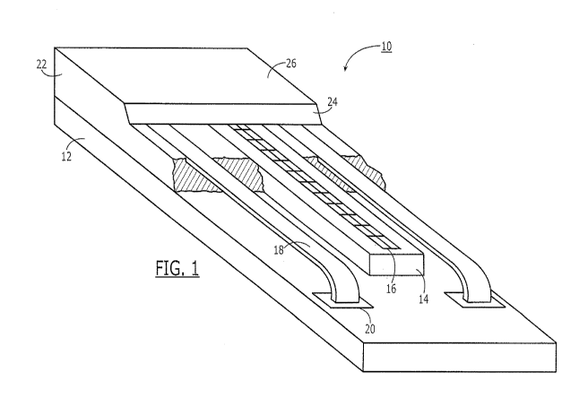
[0015] Fig. 1 is a partial cut-away perspective view of a biometric sensor
assembly with integrally molded bezel and sensor die according to a first
embodiment
of the present disclosure.
[0016] Figs. 2A and 2B are side elevation views of two different bezels
located
on a substrate according to two embodiments of the present disclosure.
[0017] Fig. 3A is a perspective view and Figs. 3B and 3C are side elevation
and front views, respectively, of a bezel frame according to an embodiment of
the
present disclosure.
[0018] Fig. 4 is a top or plan view of a biometric sensor with integrally
molded
bezel and sensor die according to another embodiment of the present
disclosure.
[0019] Fig. 5 is a top or plan view of the biometric sensor with integrally
molded bezel and sensor die illustrated in Fig. 1.
[0020] Fig. 6 is a front elevation view of the biometric sensor with
integrally
molded bezel and sensor die illustrated in Fig. 1.
[0021] Figs. 7A through 7C are side elevation views of three different
embodiments, respectively, of a biometric sensor with integrally molded bezel
and
sensor die according to various embodiments of the present disclosure.
[0022] Figs. 8A and 8B are a top plan view and side elevation view of another
embodiment of a biometric sensor with integrally molded bezel and sensor die
according to the present disclosure.
[0023] Fig. 9 is a top plan view of an area-based biometric sensor with
integrally molded bezel and sensor die according to another embodiment of the
present disclosure.
[0024] Fig. 10 is a top plan view of an area-based biometric sensor with
integrally molded bezel and sensor die according to yet another embodiment of
the
present disclosure.
WO 2011/109694 PCTIUS2011/027156
CA 02791
Detailed Description of the Preferred Embodiments
[0025] We initially point out that description of well-known starting
materials,
processing techniques, components, equipment and other well-known details are
merely summarized or are omitted so as not to unnecessarily obscure the
details of
the present invention. Thus, where details are otherwise well known, we leave
it to
the application of the present invention to suggest or dictate choices
relating to those
details.
[0026] With reference first to Fig. 1, there is shown therein a partial cut-
away
perspective view of a biometric sensor assembly 10 according to a first
embodiment.
Assembly 10 comprises a substrate 12, which may be a printed circuit board
(PCB),
ceramic body, or similar structure having formed thereon, and possibly in
layers
thereof, interconnection leads (not shown). Secured to substrate 12 in a die-
receiving region is sensor integrated circuit, or die, 14. Die 14 is typically
a
semiconductor body have one or more layers formed thereon, including
electrical
devices such as transistors, capacitors, interconnections and the like formed
photolithographically or by other semiconductor manufacturing processes.
Specifically, die 14 has formed thereon a two-dimensional array 16 of sensor
pixels
and sensing circuitry. Die 14 may be physically connected to substrate 12 by
an
adhesive between the bottom side of die 14 and the top side of substrate 12,
and
electrically connected by a plurality of wirebonds from the top side of die 14
to the top
side of substrate 12. Other methods may also be employed as well known in the
art..
[0027] One or more bezels 18 are secured to bezel receiving regions 20 on
substrate 12. Bezels 18 may be discrete individual elements, or may form part
of a
bezel frame (described further below). Bezels 18 may be opaque, conductive
elements used, for example, to inject current into the finger of a user as the
finger is
being sensed by the pixels of two-dimensional array 16. In the embodiment
shown in
Fig. 1, bezels 18 are discrete arch (or inverted "U") shaped metal structures,
which
may be individually secured to bezel receiving regions 20. It should be noted
that
Fig. 1 is a partial cut-away of a completed structure and that each bezel in
this
embodiment has at least one, and typically two points of contact with
substrate 12.
Thus, one such point of contact is shown in the cut-away portion, while the
other is
6
WO 2011/109694 PCT/US2011/027156
CA 02]91
within the portion of encapsulation structure 22 shown in the Fig. 1, and thus
not
shown. Optionally, bezels 18 may be provided with visual indicator regions
(not
shown) and a light source (also not shown) associated with assembly 10, as
described further in the aforementioned application for U.S. Letters Patent
serial
number [not yet assigned].
[0028] Die 14 and bezel 18 are embedded within encapsulation structure 22
such that a top surface of die 14, and in particular array 16, as well as a
top surface
of bezel 18 are at least partly exposed to a user. These top surfaces are
either
coplanar or are in closely spaced apart, parallel planes. Regions of these
surfaces
may be left uncovered by the material forming encapsulation structure 22, for
example by masking over those regions during formation of the encapsulation
structure 22. One or both of the top surface of array 16 and bezel 18 may
alternatively be very thinly covered by material forming encapsulation
structure 22, or
by other coating material, in order to provide physical protection of the
array and/or
bezel surface, but such that capacitive sensing of the fingerprint pattern
and/or
conduction between bezel 18 and the user's finger is nevertheless enabled.
[0029] The material forming encapsulation structure 22 may be an insulative,
semi-transparent or opaque resin or plastic of a type otherwise well known in
the art.
Encapsulation may be accomplished by transfer molding or other techniques. One
of
a variety of integrated circuit molding techniques known in the art may be
employed
to form encapsulation structure 22. According to one example of these
techniques,
disclosed in U.S. patent 6,686,227, which is incorporated herein by reference,
the die
is mounted to the substrate, with bonding wires (described further with
reference to
Fig. 5) making electrical connection between the die and substrate. The die
and
substrate are placed in a mold body, such that the mold body clamps the
substrate to
hold the assembly in place. Encapsulation material is injected into the mold
body. A
seal blocks encapsulation material injected into the mold from being applied
to the
region of surfaces that are desirably to be exposed, in the present case the
upper
surfaces of die 14 and bezel 18. The binding wires are encased in the
encapsulation
material for protection, and the regions thereover become tapered guide
regions 24
and shelf regions 26. By including bezels 18 within the mold body in the
molding
7
WO 2011/109694 PCT/US2011/027156
CA 02]91
process, and positioning the upper surfaces of bezels 18 generally co-planar
or in a
plane parallel with the place of upper surface of die 14, the molding process
may
effectively encapsulate both die 14 and bezel 18 within encapsulation
structure 22 yet
provide the desired exposed surface regions of die 14 and bezel 18.
[0030] Encapsulation structure 22 will substantially cover the top surface of
substrate 12. It may also extend to the sides of substrate 12. The back side
of
substrate 12 may be provided with conductive bump contacts (e.g., ball grid
array or
land grid array, not shown) for back-side interconnection to a printed circuit
board or
other component mounting assembly as part of final device construction.
Alternatively, the back side or top side of substrate 12 may be provided with
contact
pads or pins, which are left exposed following the molding process to permit
electrical
interconnection of the molded subassembly within another electrical system. A
complete biometric sensor assembly with integrally molded bezel and sensor die
is
thus obtained.
[0031] The description above of a biometric sensor includes one or more
bezels 18 mounted to substrate 12. Fig. 2A illustrates one exemplary
embodiment of
a bezel 18a having an arch (or inverted "U") shape when viewed from the side.
Fig.
2B illustrates another exemplary embodiment of a bezel 18b which is a solid
rectangular structure, for example with rounded corners, when viewed from the
side.
While the specific cross-sectional shape of bezel 18 in no way limits the
scope of the
present disclosure, the present disclosure is unique in that a structure and
method
making that structure are provided in which a bezel located proximate sensor
circuitry
is unitarily disposed within an encapsulation structure. Physical and
environmental
protection of the structural elements of the assembly is provided by the
encapsulation
structure. Furthermore, the bezel may be located much closer to the sensor die
than
heretofore possible.
[0032] While the embodiment shown in Fig. 1 includes two bezels 18, each
individually and discretely located on substrate 12, according to one
variation of the
disclosure herein, only a single bezel is employed. According to one further
variation,
the bezel(s) may form a portion of an integrated lead frame and bezel
structure as
described in application for United States Letters Patent serial number
12/324,869,
8
WO 2011/109694 PCT/US2011/027156
CA 02]91
which is incorporated herein by reference. An example of such a bezel frame 60
is
illustrated in Figs. 3A, 3B, and 3C. Bezel frame 60 includes first bezel 62
and second
bezel 64, with connecting arms 66 connecting bezels 62, 64 to contact and
bonding
pads 68. Again, one or more than two bezels may similarly be provided,
although
such embodiments are not separately illustrated.
[0033] In the case of a single bezel or a plurality of bezels integrally
molded
with the sensor die, the bezel(s) may be adjacent a side(s) of the sensor die.
Again,
due to the fact that the bezel(s) is positioned relative to the sensor die
prior to the
molding of the sensor die, the bezel(s) may be made closer to the sensor die
than
heretofore possible.
[0034] While described above as being located proximate the sides of the
sensor die, the bezel(s) may fully surround the sensor die. For example, the
bezel
may be closed structure, such as a rectangle, oval, etc. having an opening in
its
center in which the sensor die is positioned. This embodiment is illustrated
in Fig. 4,
in which a substrate 30 has secured thereto a sensor die 32 and a closed bezel
structure 34, in this case of rectangular planform, having an opening 36 in
which
sensor die 32 is disposed and through which the upper surface of sensor die 32
is
presented. The entirety of the surface of substrate 30 to which sensor die 32
and
bezel 34 are secured is covered with encapsulation material (not shown),
leaving the
top surfaces of sensor die 32 and bezel 34 exposed or at most thinly covered
by the
encapsulation material.
[0035] With reference to Figs. 5, 6, and 7A through 7C, there is shown therein
a plan view and a number of cut-away cross-sectional views, respectively, of a
integrally molded die and bezel structure for fingerprint sensors and the like
according to an embodiment of the present invention. More specifically, Fig. 5
is a
plan view of the biometric sensor assembly 10 shown in perspective view in
Fig. 1.
Fig. 6 is a cut-away cross sectional view of assembly 10, viewed in the axial
direction
of a user's finger 38. As can be seen from Fig. 6, die 14 is physically
mounted to
substrate 12, and electrically connected thereto by wirebonds 28.
Alternatively, die
14 may be physically and electrically connected to substrate 12 by adhesive
and
wirebonds, respectively. Die 14, bezels 18, wirebonds 28, etc. are molded so
as to
9
WO 2011/109694 PCT/US2011/027156
CA 02]91
protect wirebonds 28 and portions of die 14 and bezels 18 under guide regions
24
and shelf regions 26. Importantly, as molded, a portion of the upper surface
of die
14, e.g., sensor die 16, is exposed to permit physical contact with finger 38.
The
encapsulation material may also thinly cover this region of die 14 provided
the
operational principles (e.g., capacitive sensing) on which the sensing
function of
sensor die 16 operates is not significantly degraded.
[0036] With reference to Figs. 7A through 7C, various embodiments of the
elevation of bezels 18 relative to the top surface of die 14 can be seen. In
embodiment 40 shown in Fig. 7A, the molding may be such that the top surface
of
bezel 18 and the top surface of die 14 are coplanar. In this embodiment, the
molding
is further controlled such that the top surfaces of die 14 and bezels 18 are
exposed
(i.e., not covered by encapsulation material) so that a user's finger (not
shown) may
by in physical contact therewith. Alternatively, in embodiment 42 shown in
Fig. 7B,
while the planes of the top surfaces of the die 14 and bezel 18 are coplanar,
the
molding is controlled so that a thin layer of encapsulation material 44
(thickness t) is
formed thereover, for example for physical protection of the sensor die 16
and/or
bezel 18.
[0037] In embodiment 46 shown in Fig. 7C, the plane of the top surface of
die14 and the plane of the top surface of bezels 18 are not coplanar. The
plane of
the top surface of bezels 18 is slightly above the plane of the top surface of
die 14 (by
distance c). In this case, the top surface of bezels 18 may protrude slightly
above the
encapsulation material 22, for example to improve physical contact therewith
by a
user's finger (not shown). Also in this case, it may be desirable to provide
bezels 18
with a slightly rounded top surface (shown in cross-section in Fig. 7C) or
corners for
user comfort, for device robustness, to avoid the buildup of contaminants at
the bezel
edge, etc.
[0038) In embodiment 80 shown in Figs. 8A and 8B, a substrate 82 has
physically connected thereto a die 84. The connection may also be electrical,
as
described above. Die 84 has formed therein a sensor region 86, also as
described
above. A bezel 88 is also physically, and optionally electrically, connected
to
substrate 82. In embodiment 80, only a single bezel 88 is provided, as
compared for
WO 2011/109694 PCT/US2011/027156
CA 02]91
example to embodiment 10 shown in Fig. I in which two bezels 18 are shown.
Finally, as previously described, die 84 and bezel 88 are surrounded by
encapsulation material 90, which is molded to form, for example, tapered guide
regions 92 and shelf regions 94. Again, die 84 and bezel 88 are embedded
within
encapsulation structure 90 such that a top surface of die 84, and in
particular array
86, as well as a top surface of bezel 88 are at least partly exposed to a
user.
Alternatively, the top surfaces of die 84 and bezel 88 may be thinly covered
by
encapsulation material.
[0039] The foregoing description has assumed that the sensor device is of a
type that is, when viewed from above, approximately the width of an average
user's
fingertip, but only several pixels tall, typically between 1 and 8 pixels, and
possibly as
many as 16 pixels tall. Such sensors are typically referred to as strip
sensors. In
operation, a user swipes a finger over a surface of the sensor. The sensor
captures
a number of thin strips of the fingerprint as the finger is swiped, and the
complete
fingerprint is assembled in software for use in authentication. Such a sensor
apparatus is typically preferred when a compact sensor is desired. However,
the
present disclosure is not limited to strip sensors. For example, with
reference to Fig.
9, there is shown therein an embodiment 100 of an integrally molded bezel and
sensor die wherein the sensor is of a type that is, when viewed from above,
approximately the width and length of an average user's fingertip. In
operation, the
user holds their fingertip in place over the sensor area, and the fingerprint
is scanned,
typically in raster fashion. Such sensors are typically referred to as area
sensors.
For illustration purposes, embodiment 100 comprises a single bezel 102 and an
area
sensor die 104, integrally molded in an encapsulation structure 106. It will,
however,
be appreciated that more than one bezel 102 can be used in a similar
embodiment.
Similarly, a second area sensor embodiment 110 is shown in Fig. 10, in which a
bezel 112 in the form of a rectangular ring fully surrounds an area sensor die
114,
integrally molded in an encapsulation structure 116.
[0040] Accordingly, various embodiment of an integrally molded die and bezel
structure for fingerprint sensors and the like have been disclosed. These
various
embodiments highlight the scope and breadth of the claims that follow.
However, the
11
WO 2011/109694 PCT/US2011/027156
CA 02791
physics of modern electrical devices and the methods of their production are
not
absolutes, but rather statistical efforts to produce a desired device and/or
result.
Even with the utmost of attention being paid to repeatability of processes,
quality of
starting and processing materials, and so forth, variations and imperfections
result.
Accordingly, no limitation in the description of the present disclosure or its
claims can
or should be read as absolute. The limitations of the claims are intended to
define
the boundaries of the present disclosure, up to and including those
limitations. To
further highlight this, the term "substantially" may occasionally be used
herein and in
association with a claim limitation (although consideration for variations and
imperfections is not restricted to only those limitations used with that
term). While as
difficult to precisely define as the limitations of the present disclosure
themselves, we
intend that this term be interpreted as "to a large extent", "as nearly as
practicable",
"within technical limitations", and the like.
[0041] Furthermore, while a plurality of exemplary embodiments have been
presented in the foregoing detailed description, it should be understood that
a vast
number of variations exist, and these exemplary embodiments are merely
representative examples, and are not intended to limit the scope,
applicability or
configuration of the disclosure in any way. Various of the above-disclosed and
other
features and functions, or alternative thereof, may be desirably combined into
many
other different arrangements or embodiments, and potentially find alternative
applications. Further still, various presently unforeseen or unanticipated
alternatives,
modifications variations, or improvements therein or thereon may be
subsequently
made by those skilled in the art which are also intended to be encompassed by
the
claims, below.
[0042] Therefore, the foregoing description provides those of ordinary skill
in
the art with a convenient guide for implementation of the disclosure, and
contemplates that various changes in the functions and arrangements of the
described embodiments may be made without departing from the spirit and scope
of
the disclosure defined by the claims thereto.
12