Note: Descriptions are shown in the official language in which they were submitted.
81731858
1
ELECTRONIC CONTROL UNIT
BACKGROUND OF THE INVENTION
The present invention relates to an electronic control unit.
Priority is claimed on Japanese Patent Application No. 2011-231805, filed on
October 21, 2011.
Field of the Invention
In recent years, vehicles (hereinafter, collectively referred to as plug-in
vehicles)
such as electric cars or plug-in hybrid cars that can be charged by the use of
an external
power supply have been increasingly put to practical use. A dedicated charging
cable
having a control unit called a CC1D (Charge Circuit Interrupt Device) is used
to connect
a plug-in vehicle to an external power supply.
The standard on an interface between the charging cable and the plug-in
vehicle
is defined by the "SAE (Electric Vehicle Conductive Charge Coupler) standard"
of the
U.S. or the "General Requirements for Electric Vehicle Conductive Charging
System (the
Japanese Electric Vehicle Standard)" of Japan. The charging sequence of a plug-
in
vehicle defined in the standard is substantially as follows.
First, a CCTD of a charging cable transmits a control pilot signal
(hereinafter,
abbreviated as a pilot signal) to a charging-control ECU (Electronic Control
Unit)
mounted on a plug-in vehicle and determines that the charging cable is
connected to the
plug-in vehicle when the voltage of the pilot signal is changed from an
initial value VI
(for example, 12 V) to V2 (for example, 9 V),
Then, the CCID of the charging cable informs the ECU of the plug-in vehicle of
the rated current of a power supply facility by transmitting a pilot signal
with a duty ratio
CA 2792279 2018-10-17
CA 02792279 2012-10-15
2
corresponding to the rated current of the power supply facility (including an
external
power supply and a charging cable).
Subsequently, the ECU of the plug-in vehicle informs the CCID of the charging
cable of completion of the preparation for charging by changing the voltage of
the pilot
signal from V2 to V3 (for example, 6 V).
Then, when detecting that the voltage of the pilot signal has changed from V2
to
V3, the CCID of the charging cable determines that the preparation for
charging of the
plug-in vehicle side is completed, and turns on a relay used to supply the
power of the
external power supply to the plug-in vehicle (that is, starts the supply of
power).
In this way', the pilot signal is a signal essential for controlling the
charging of
the plug-in vehicle and it is very important to detect abnormality of the
pilot signal. For
example, Japanese Unexamined Patent Application, First Publication No. 2009-
71989
discloses a technique of detecting a disconnection of a control line used for
transmission
of a pilot signal in a state where a plug-in vehicle is connected to an
external power
supply via a charging cable.
Description of the Related Art
As described in Japanese Unexamined Patent Application, First Publication No.
2009-71989, the pilot signal is input to a CPU (Central Processing Unit) via
an input
buffer in an ECU of the plug-in vehicle. Since a recommended input voltage
range is
determined for the input buffer but the voltage of the pilot signal varies in
a broad range,
the input buffer may not work normally or the input buffer may be destroyed in
a worst
case. Accordingly, a circuit for protecting the input buffer is necessary, but
such a
circuit is not disclosed in Japanese Unexamined Patent Application, First
Publication No.
2009-71989.
CA 02792279 2012-10-15
3
The invention is made in consideration of the above-mentioned circumstances
and an object thereof is to provide an electronic control unit that can
protect an input
buffer for a pilot signal, which a pilot signal is input to, disposed in a
stage preceding a
processor such as a CPU when a plug-in vehicle is charged from an external
power
.. supply via a charging cable.
SUMMARY OF THE INVENTION
The present invention employs the following configurations to solve the above
problems.
(1) According to an aspect of the invention, there is provided an
electronic control
unit that is mounted on a vehicle which is configured to be charged with an
external
power supply and that receives a pilot signal via a charging cable before
being supplied
with a power when the vehicle is connected to the external power supply via
the charging
cable, the electronic control unit including: a pilot voltage setting circuit
that changes a
.. voltage of the pilot signal in a stepwise manner; a processor that performs
a process
necessary for a control of charging based on the pilot signal, and that
controls the pilot
voltage setting circuit to change the voltage of the pilot signal; an input
buffer that is
disposed in a stage preceding a pilot signal input port of the processor; and
an input
buffer voltage setting circuit that changes the input voltage of the input
buffer so as to be
within a recommended input voltage range of the input buffer based on the
change in the
voltage of the pilot signal.
(2) In the electronic control unit described in (I) above, the input
buffer voltage
setting circuit may be a resistance-type voltage division circuit of which a
division ratio
can be switched and may change the input voltage of the input buffer so as to
be within
the recommended input voltage range of the input buffer by switching the
division ratio
81731858
4
of the resistance-type voltage division circuit based on the change in the
voltage of the pilot
signal.
(3) In the electronic control unit described in (2) above, the pilot
voltage setting circuit may
include: a pull-down resistor of which one end thereof is connected to a pilot
signal line extending
from a pilot signal input terminal of the electronic control unit to the input
buffer; and a first
switching element that is connected between other end of the pull-down
resistor and a ground and
that is switched between ON and OFF states based on a control signal output
from the processor,
and the input buffer voltage setting circuit may include: a first voltage-
dividing resistor that is
disposed in the pilot signal line in a stage following the pilot voltage
setting circuit; a second
voltage-dividing resistor of which one end thereof is connected to the pilot
signal line between the
first voltage-dividing resistor and the input buffer; a third voltage-dividing
resistor of which one
end thereof is connected to other end of the second voltage-dividing resistor
and other end is
connected to the ground; a level inverter circuit that receives the control
signal output from the
processor and that inverts and outputs the level of the control signal; and a
second switching
element that is connected in parallel to the third voltage-dividing resistor
and that is switched
between ON and OFF states based on the control signal output from the level
inverter circuit.
According to another aspect of the present disclosure, there is provided an
electronic
control unit that is mounted on a vehicle which is configured to be charged
with an external power
supply and that receives a pilot signal via a charging cable before being
supplied with a power
when the vehicle is connected to the external power supply via the charging
cable, the electronic
control unit comprising: a processor that performs a process necessary for
control of charging
based on the pilot signal; an input buffer that is disposed in a stage
preceding a pilot signal input
port of the processor; a pilot voltage setting circuit that changes a voltage
of the pilot signal in a
stepwise manner depending on a control signal output from the processor while
the vehicle, the
charging cable, and the external power supply are connected; and an input
buffer voltage setting
circuit that is a division circuit which divides the voltage of the pilot
signal, and that has an output
terminal connected to an input terminal of the input buffer; wherein a
division ratio of the input
CA 2792279 2018-10-17
81731858
4a
buffer voltage setting circuit is switched depending on the control signal so
that an input voltage
of the input buffer is set to be within a recommended input voltage range of
the input buffer;
wherein the pilot voltage setting circuit, the input buffer voltage setting
circuit, the input buffer,
and the processor are arranged in a line in this order.
According to another aspect of the present disclosure, there is provided an
electronic
control unit that is mounted on a vehicle which is configured to be charged
with an external power
supply and that receives a pilot signal via a charging cable before being
supplied with a power
when the vehicle is connected to the external power supply via the charging
cable, the electronic
control unit comprising: a processor that performs a process necessary for
control of charging
based on the pilot signal; an input buffer that is disposed in a stage
preceding a pilot signal input
port of the processor; a pilot voltage setting circuit that changes a voltage
of the pilot signal in a
stepwise manner depending on a control signal output from the processor while
the vehicle, the
charging cable, and the external power supply are connected; and an input
buffer voltage setting
circuit that is a division circuit which divides the voltage of the pilot
signal, and that has an output
terminal connected to an input terminal of the input buffer; wherein a
division ratio of the input
buffer voltage setting circuit is switched depending on the control signal so
that an input voltage
of the input buffer is set to be within a recommended input voltage range of
the input buffer;
wherein the pilot voltage setting circuit comprises: a pull-down resistor of
which one end thereof
is connected to a pilot signal line extending from a pilot signal input
terminal of the electronic
control unit to the input buffer; and a first switching element that is
connected between other end
of the pull-down resistor and a ground and that is switched between ON and OFF
states based on a
control signal output from the processor, and wherein the input buffer voltage
setting circuit
comprises: a first voltage-dividing resistor that is disposed in the pilot
signal line in a stage
following the pilot voltage setting circuit; a second voltage-dividing
resistor of which one end
thereof is connected to the pilot signal line between the first voltage-
dividing resistor and the input
buffer; a third voltage-dividing resistor of which one end thereof is
connected to other end of the
second voltage-dividing resistor and other end is connected to the ground; a
level inverter circuit
CA 2792279 2018-10-17
81731858
4b
that receives the control signal output from the processor and that inverts
and outputs the level of
the control signal; and a second switching element that is connected in
parallel to the third
voltage-dividing resistor and that is switched between ON and OFF states based
on the control
signal output from the level inverter circuit.
BRIEF DESCRIPTION OF THE DRAWINGS
FIG. 1 is a schematic diagram illustrating a vehicle charging system according
to an
embodiment of the invention.
FIG. 2 is a diagram illustrating the internal configuration of a charging-
control ECU 33
mounted on a plug-in vehicle 3.
FIG. 3 is a timing diagram illustrating the operation of the vehicle charging
CA 2792279 2018-10-17
CA 02792279 2012-10-15
system.
DETAILED DESCRIPTION OF THE INVENTION
Hereinafter, an embodiment of the invention will be described in detail with
5 reference to the accompanying drawings.
FIG. 1 is a schematic diagram illustrating a vehicle charging system according
to
an embodiment of the invention. As shown in FIG. 1, the vehicle charging
system
according to this embodiment includes an external power supply 1, a charging
cable 2,
and a plug-in vehicle 3. The external power supply I includes a power
receptacle 11
with a ground terminal disposed, for example, in a house and an AC power
supply
(commercial power supply) 12 supplying single-phase AC power to the power
receptacle
11.
The charging cable 2 includes two power supply lines 21 and 22, aground line
23, a pilot line 24, a plug 25, a cable-side coupler 26, and a CCID 27. In
each of the
.. power supply lines 21 and 22 and the ground line 23, an end thereof is
connected to the
plug 25 and the other end thereof is connected to the cable-side coupler 26.
An end of
the pilot line 24 is connected to the CCID 27 (specifically, a pilot circuit
27c) and the
other end thereof is connected to the cable-side coupler 26.
By connecting the plug 25 to the power receptacle 11, one end of each of the
power supply lines 21 and 22 is connected to the AC power supply 12 and one
end of the
ground line 23 is connected to the ground of the external power supply I. By
connecting the cable-side coupler 26 to a vehicle-side coupler 31 of the plug-
in vehicle 3,
the other end of each of the power supply lines 21 and 22 is connected to a
battery
charger 32 of the plug-in vehicle 3 and the other end of each of the ground
line 23 and
the pilot line 24 is connected to a charging-control ECU 33 of the plug-in
vehicle 3.
CA 02792279 2012-10-15
6
The CC1D 27 is a control unit that is disposed in the middle of the power
supply
lines 21 and 22 and the ground line 23, and includes relays 27a and 27b
disposed in the
middle of the power supply lines 21 and 22 and a pilot circuit 27c
transmitting a pilot
signal CPL to the charging-control ECU 33 of the plug-in vehicle 3 via the
pilot line 24
and controlling ON and OFF states of the relays 27a and 27b. The pilot circuit
27c is
connected to the power supply lines 21 and 22 and the ground line 23 and is
supplied
with a source voltage from the power supply lines 21 and 22 and with a ground
voltage
from the ground line 23.
The plug-in vehicle 3 is a vehicle which can be charged with the external
power
.. supply 1, such as an electric car or a plug-in hybrid car, and includes a
vehicle-side
coupler 31, a battery charger 32, and a charging-control ECU 33. By connecting
the
cable-side coupler 26 of the charging cable 2 to the vehicle-side coupler 31,
the power
supply lines 21 and 22 are connected to the battery charger 32, and the ground
line 23
and the pilot line 24 are connected to the charging-control ECU 33.
The battery charger 32 is a charging circuit that converts single-phase AC
power
supplied from the external power supply 1 via the charging cable 2 (the power
supply
lines 21 and 22) into DC power under the control of the charging-control ECU
33 and
that charges a driving battery (not shown) mounted on the plug-in vehicle 3
with the DC
power. The charging-control ECU 33 is an electronic control unit that receives
a pilot
.. signal CPL via the charging cable 2 before being supplied with the power
when the
plug-in vehicle 3 is connected to the external power supply I via the charging
cable 2 and
that performs a process necessary for the charging control of the driving
battery based on
the pilot signal CPL.
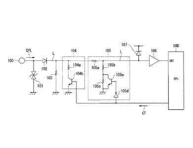
FIG. 2 is a diagram illustrating the internal configuration of the charging-
control
ECU 33. As shown in FIG. 2, the charging-control ECU 33 includes a pilot
signal input
CA 02792279 2012-10-15
7
terminal 100, an avalanche diode 101, a first diode 102, a first pull-down
resistor 103, a
pilot voltage setting circuit 104, an input buffer voltage setting circuit
105, an input
buffer 106, a second diode 107, and a CPU 108.
The pilot signal input terminal 100 is an external input terminal that is
connected
to the pilot line 24 when the cable-side coupler 26 of the charging cable 2 is
connected to
the vehicle-side coupler 31. The avalanche diode 101 has one end connected to
the
pilot signal input terminal 100 and the other end connected to the ground and
serves to
maintain the voltage of the pilot signal CPL (the voltage between the pilot
signal input
terminal 100 and the ground) input via the pilot signal input terminal 100 at
Vi (for
.. example, 12 V) or lower.
The first diode 102 has an anode terminal connected to the pilot signal input
terminal 100 and a cathode terminal connected to one end of the first pull-
down resistor
103 and serves to pass only a positive signal of the pilot signal CPL. The
first
pull-down resistor 103 has one end connected to the cathode terminal of the
first diode
102 and the other end connected to the ground and serves to change the
positive voltage
of the pilot signal CPL (that is, the voltage between the cathode terminal of
the first diode
102 and the ground) from Vito V2 (for example, 9 V).
The pilot voltage setting circuit 104 is a circuit that changes the positive
voltage
of the pilot signal CPL in a stepwise manner (for example, changes the voltage
from V2
to V3 (for example, 6 V)) under the control of the CPU 108. The pilot voltage
setting
circuit 104 includes a second pull-down resistor 104a of which one end is
connected to
the cathode terminal of the first diode 102 (connected to the pilot signal
line L extending
from the pilot signal input terminal 100 to the input buffer 106) and a first
switching
element (for example, a transistor) 104b that is connected between the other
end of the
second pull-down resistor 104a and the ground and that is switched between ON
and
CA 02792279 2012-10-15
8
OFF states depending on a control signal CT output from the CPU 108.
In the pilot voltage setting circuit 104 having this configuration, when the
first
switching element 104b is in ON state, the other end of the second pull-down
resistor
104a is connected to the ground and the positive voltage of the pilot signal
CPL is
changed from V2 to V3.
The input buffer voltage setting circuit 105 is a resistance-type voltage
division
circuit of which the division ratio can be switched and is a circuit that
changes the input
voltage of the input buffer 106 to he within a recommended input voltage range
(for
example, a range of 3.5 to 5.5 V) of the input buffer 106 by switching the
division ratio
of the resistance-type voltage division circuit depending on the change in
voltage of the
pilot signal CPL.
Specifically, the input buffer voltage setting circuit 105 includes a first
voltage-dividing resistor 105a disposed in the middle of the pilot signal line
L in a stage
following the pilot voltage setting circuit 104, a second voltage-dividing
resistor 105b of
which an end is connected to the pilot signal line L between the first voltage-
dividing
resistor 105a and the input buffer 106, a third voltage-dividing resistor
10.50 of which one
end is connected to the other end of the second voltage-dividing resistor 105b
and the
other end is connected to the ground, a level inverter circuit 105d that
receives the
control signal CT output from the CPU 108 and that inverts and outputs the
level of the
control signal CT, and a second switching element (for example, a transistor)
105e that is
connected in parallel to the third voltage-dividing resistor 105c and that is
switched
between ON and OFF states depending on the inverted control signal CT output
from the
level inverter circuit 105d.
In the input buffer voltage setting circuit 105 having this configuration,
when the
positive voltage of the pilot signal CPL is V2 (9 V), the first switching
element I04b is in
CA 02792279 2012-10-15
9
OFF state and thus the second switching element 105e is switched to ON state.
Here,
when the resistance value of the first voltage-dividing resistor 105a is
defined as R1, the
resistance value of the second voltage-dividing resistor 105b is defined as
R2, and the
resistance value of the third voltage-dividing resistor 105c is defined as R3,
the division
ratio when the second switching element 105e is in ON state is expressed by
R2/(RI+R2).
By the use of this division ratio, the resistance values RI and R2 are set
such that the
input voltage of the input buffer 106 (the voltage between one end of the
second
voltage-dividing resistor 105b and the ground) is equal to or lower than 5.5 V
which is
the maximum value of the recommended input voltage range of the input buffer
106.
On the other hand, when the positive voltage of the pilot signal CPL is V3 (6
V),
the first switching element 104b is in ON state and thus the second switching
element
105e is switched to OFF state. The division ratio when the second switching
element
105e is in OFF state is expressed by (R2+R3)/(RI+R2+R3). By the use of this
division
ratio, the resistance values RI, R2, and R3 are set such that the input
voltage of the input
buffer 106 is equal to or higher than 3.5 V which is the minimum value of the
recommended input voltage range of the input buffer 106.
The input buffer 106 is a buffer of which an input terminal is connected to
the
other end of the first voltage-dividing resistor 105a and one end of the
second
voltage-dividing resistor 105b and an output terminal is connected to a pilot
signal input
port INT of the CPU 108 (that is, disposed in a stage preceding the pilot
signal input port
INT of the CPU 108). As described above, for example, a recommended input
voltage
range of 3.5 to 5.5 V is determined for the input buffer 106. The pilot signal
CPL is
input to the CPU 108 via the input buffer 106.
The second diode 107 has an anode terminal connected to the input terminal of
the input buffer 106 and a cathode terminal connected to the power supply
line. The
CA 02792279 2012-10-15
second diode 107 is provided to clamp and protect the input voltage of the
input buffer
106 so as not to be greater than the maximum rated voltage (for example, 7 V).
The CPU 108 is a processor that performs a process necessary for the charging
control and controls the pilot voltage setting circuit 104 and the input
buffer voltage
5 setting circuit 105 (outputs the control signal CT) to change the voltage
of the pilot signal
CPL, based on the pilot signal CPL input to the pilot signal input port INT
via the input
buffer 106.
The operation of the vehicle charging system having the above-mentioned
configuration will be described below with reference to the timing diagram of
FIG 3.
10 First, at time ti in FIG. 3, when the plug 25 of the charging cable 2 is
connected
to the power receptacle 11 of the external power supply 1, the pilot circuit
27c of the
CCID 27 is supplied with power from the AC power supply 12 via the power
supply lines
21 and 22, is started up, and outputs the pilot signal CPL of a voltage value
VI (12 V) via
the pilot line 24. At this time point, the relays 27a and 27b of the CCID 27
are in OFF
state and the CPU 108 of the charging-control ECU 33 is in a sleep state.
As shown in FIG. 3, when the CPU 108 is in the sleep state, the control signal
CT output from the CPU 108 is at a low level. Accordingly, the first switching
element
104b of the pilot voltage setting circuit 104 is in OFF state and the second
switching
element 105e of the input buffer voltage setting circuit 105 is in ON state.
Subsequently, at time t2 in FIG. 3, when the cable-side coupler 26 of the
charging cable 2 is connected to the vehicle-side coupler 31 of the plug-in
vehicle 3, the
pilot signal CPL is input to the pilot signal input terminal 100 of the
charging-control
ECU 33, but the positive voltage of the pilot signal CPL (the voltage between
the cathode
terminal of the first diode 102 and the ground) is changed from Vito V2 (9 V)
by the
first pull-down resistor 103.
CA 02792279 2012-10-15
II
In this way, after time t2, the positive voltage of the pilot signal CPL (the
voltage between the cathode terminal of the first diode 102 and the ground)
input to the
charging-control ECU 33 is V2 (9 V). However, since the first switching
element 104b
is in OFF state and the second switching element 105e is in ON state, the
division ratio of
the input buffer voltage setting circuit 105 is R2/(R1+R2) and the input
voltage of the
input buffer 106 is suppressed to be equal to or less than 5.5 V which is the
maximum
value of the recommended input voltage range of the input buffer 106.
When the change in voltage of the pilot signal CAL (the change in voltage of
the
pilot line 24) is detected, the pilot circuit 27c of the CC1D 27 determines
that the
charging cable 2 is connected to the plug-in vehicle 3 and informs the
charging-control
ECU 33 of the rated current of the power supply facility by transmitting the
pilot signal
CPL at a duty ratio corresponding to the rated current of the power supply
facility (the
external power supply 1 and the charging cable 2) at time 13 in FIG. 3.
When the CPU 108 of the charging-control ECU 33 starts up from the sleep
.. state at time t4 in a predetermined time after time 13, the CPU 108
measures the duty
ratio of the pilot signal CPL input via the input buffer 106 to acquire the
rated current of
the power supply facility, then outputs the control signal CT of a high level
at time t5 in
FIG. 3 to switch the first switching element 104b to ON state (to switch the
second
switching element 105e to OFF state) and to change the voltage of the pilot
signal CPL
from V2 to V3 (6 V), whereby the COD 27 of the charging cable 2 is informed of
the
completion of the preparation for charging.
In this way, after time 15, the positive voltage of the pilot signal CPL (the
voltage between the cathode terminal of the first diode 102 and the ground)
input to the
charging-control ECU 33 becomes V3 (6 V), However, as described above, since
the
first switching element 104b is in ON state and the second switching element
105e is in
CA 02792279 2012-10-15
12
OFF state, the division ratio of the input buffer voltage setting circuit 105
is
(R2+R3)/(R1+R2+R3) and the input voltage of the input buffer 106 increases to
be equal
to or higher than 3.5 V which is the minimum value of the recommended input
voltage
range of the input buffer 106.
When the pilot circuit 27c of the CCID 27 detects that the voltage of the
pilot
signal CPL (the voltage of the pilot line 24) has changed from V2 to V3, the
pilot circuit
27c determines that the preparation for charging of the plug-in vehicle 3 is
completed and
turns on the relays 27a and 27b for supplying the AC power of the external
power supply
I to the plug-in vehicle 3 (that is, starts the supply of power). Accordingly,
the AC
power is supplied from the external power supply 1 to the battery charger 32
of the
plug-in vehicle 3 via the charging cable 2 (the power supply lines 21 and 22).
The CPU 108 of the charging-control ECU 33 appropriately controls the
charging of the driving battery by controlling the battery charger 32 based on
the rated
current of the power supply facility acquired from the duty ratio of the pilot
signal CPL.
As described above, according to this embodiment, since the input voltage of
the
input buffer 106 for the pilot signal CPL disposed in the stage preceding the
CPU 108 is
set to be within the recommended input voltage range thereof depending on the
change in
voltage of the pilot signal CPL, it is possible to protect the input buffer
106 for a pilot
signal CPL when the plug-in vehicle 3 is charged with the external power
supply 1 via
the charging cable 2.
The invention is not limited to the above-mentioned embodiment, but may be
modified as follows.
For example, the embodiment employs the configuration in which the voltage of
the pilot signal CPL is automatically changed from Vito V2 at the time point
at which
the charging cable 2 is connected to the plug-in vehicle 3 (at time t2 in Fig.
3).
CA 02792279 2012-10-15
13
However, the invention is not limited to this configuration, and may employ a
configuration in which the CPU 108 is started up at the time at which the
charging cable
2 is connected to the plug-in vehicle 3, that is, when the pilot signal CPL of
a voltage
value VI is input to the charging-control ECU 33, and the voltage of the pilot
signal CPL
is changed from Vito V2 under the control of the CPU 108.