Note: Descriptions are shown in the official language in which they were submitted.
CA 02792807 2012-10-17
IMPROVED DC BUS REGULATOR
This application is a divisional application of co-pending application Serial
No.
2,743,480 filed October 15, 2009.
TECHNICAL FIELD
This disclosure generally relates to power transmission networks. More
specifically, this disclosure relates to operating a DC power system from one
or more AC
or DC power generators. Even more specifically, this disclosure relates to
regulation of
energy transfer between an AC and DC power network.
BACKGROUND OF THE INVENTION
Power transmissions networks can be made of AC systems, DC systems, or a
combination of the two. AC power networks have conventionally been used
throughout
the world. However, DC power networks have certain advantages. DC power
networks
are easier to design and implement because they introduce no reactance into
the power
system. Higher efficiencies from generators can be achieved in DC systems
because only
real power is transmitted. Additionally, parallelization of power supplies is
simple
because the operating frequency of DC power supplies is 0 Hz. Therefore, no
synchronization is required when additional supplies or loads are brought onto
the
network.
The conventional use of AC power networks is a result of the ease of
transmitting
AC power over long distances and handling voltage changes using transformers.
However, over short distances, such as those in isolated environments, a DC
power
transmission network could be beneficial for the reasons previously explained.
High-
power generators available today typically produce AC power. Therefore,
operation of a
DC transmission network powered by AC generators requires conversion from AC
to DC
and vice versa.
Reliable operation of a power network is a critical element of many electronic
systems, for example, on drilling platforms or vessels to operate onboard
thrusters.
Drilling vessels are not anchored in the ocean but are dynamically controlled
to
-1-
CA 02792807 2012-10-17
maintain a desired position in the ocean. Thrusters are used to maintain a
position within
specified tolerances of a drilling apparatus. Thrusters are propeller drives
which can have
variable rotation speed and azimuthal angle of the blades. These thrusters are
operated by
a power supply onboard the drilling vessel. Any failure of the power supply
can lead to
displacement of the vessel out of the tolerances of the drilling apparatus. In
such a case,
the drilling apparatus would need to be mechanically decoupled and recoupled
after the
power supply is restored and the position of the drilling vessel is corrected.
One method of facilitating a reliable power supply is to utilize a DC bus for
powering thrusters and other components. Such a power transmission system is
demonstrated in FIGURE 1. In such a system, the power supply is generally made
of AC
generators coupled to an AC-to-DC converter. The AC-to-DC converter places
power
from the AC generators on an intermediate DC bus. The intermediate DC bus may
be
augmented with DC generators or a battery backup system. Each motor or
thruster, as
well as other devices utilizing the intermediate DC bus, on board the drilling
vessel is
coupled to the intermediate DC bus through a DC-to-AC converter.
FIGURE 1 is a block diagram illustrating a conventional DC voltage bus
coupling
multiple AC voltage generation systems to various loads. Power system 100
includes
generators 102. Generators 102 couple to AC bus 104 through isolators 106.
Isolators
106 allow generators 102 to be removed from the bus when they are not needed
or are
malfunctioning. AC bus 104 couples to transformer 108 to condition the power
for
transmission to line 110. AC-to-DC converter 112 couples to line 110 and
converts AC
power to DC power for output onto intermediate DC bus 120. Coupled to DC bus
120 are
DC-to-AC converters 130. DC-to-AC converters 130 convert DC power to AC power
which most components are designed to use. Coupled to DC-to-AC converters 130
is line
132 to which loads may be connected. Motor 134 is coupled to line 132, and
motor 134
could be, for example, a thruster. Additionally, transformer 135 is coupled to
line 132 to
condition power for load 136. Load 136 could be, for example, a light bulb.
There are several methods for implementing the AC-to-DC converter necessary
for
placing power from the AC generators on the intermediate DC bus. These methods
conventionally employ the use of either diodes, silicon-controlled rectifiers
(SCRs), or
transistors.
-2-
CA 02792807 2012-10-17
ne apparatus for AC-to-DC power conversion is a diode rectifier (or a diode
pack).
The are several forms of diode rectifiers commonly known. One typical diode
rectifier is
a full-wave diode rectifier. The AC power systems on drilling vessels
typically utilize a
three-phase waveform such that a six diode rectifier configuration is
typically used.
Diodes conduct current only when the voltage at the anode of the diode is
greater than the
voltage at the cathode of the diode. FIGURE 2 is a schematic illustrating a
conventional
diode full-wave rectifier for three-phase AC power. Diode rectifier 200
accepts input
from three-phase AC source 202. The rectifier 200 includes diodes 204 for
rectifying the
first phase, diodes 206 for rectifying the second phase, and diodes 208 for
rectifying the
third phase. Two diodes are needed in each case to produce output from both
the positive
AC cycle and the negative AC cycle. Diodes 204, diodes 206, and diodes 208 are
coupled
between the AC source 202 and the DC bus 210. Capacitor 212 is coupled to the
DC bus
210 to average voltage ripples on DC bus 210. While rectifier 200 is shown as
a single
rectifier arrangement, several individual arrangements of one power capacity
may be
placed in parallel to create a rectifier 200 with a higher power capacity.
Diode rectifiers are commercially available from various vendors or can be
constructed by arranging individually-purchased diodes. The advantages to
diode
rectifiers are the low cost of the components. Individual diodes and complete
rectifiers are
relatively inexpensive for high-power configurations, i.e., several megawatts
(MW).
Diodes are also relatively small devices compared to other available solutions
at an
equivalent power load. Diode rectifiers, however, have no ability to regulate
the output
voltage or current. Additionally, they only conduct in one direction.
As a result of the inability to regulate output voltage or current from diode
rectifiers, SCRs, also known as thyristor rectifiers, have largely been used
in their place.
FIGURE 3 is a schematic illustrating a conventional arrangement of SCRs for
three-phase
AC-to-DC conversion. SCR pack 300 accepts input from three-phase AC source
302.
SCR pack 300 includes SCRs 304 for converting the first phase, SCRs 306 for
converting
the second phase, and SCRs 308 for converting the third phase. Each individual
SCR
includes a gate terminal 305 for accepting input. Two SCRs are needed in each
case to
produce output from both the positive AC cycle and the negative AC cycle. SCRs
304,
SCRs 306, and SCRs 308 are coupled to AC source 302 and to DC bus 310.
Capacitor
-3-
CA 02792807 2012-10-17
312 is coupled to the DC bus 310 to average ripples on DC bus 310. While SCR
pack 300
is shown as a SCR arrangement, several individual arrangements of one power
capacity
may be placed in parallel to create a SCR pack 300 with a higher power
capacity.
Output current may be regulated in the SCRs by controlling through gate
terminal
305 when in the AC cycle they turn on. SCRs also offer the low cost, small
size, and
reliability of diodes. The disadvantage of SCRs is their slow switching time
that must
occur in synchronization with the AC power supplies. As a result, they are not
well suited
to handle the power load changes experienced during instability in the power
system.
Additionally, once the SCR is turned on through gate terminal 305, it may not
be turned
off through gate terminal 305.
Transistors offer yet another solution for AC-to-DC power conversion. FIGURE 4
is a schematic illustrating a conventional arrangement of transistors for
three-phase AC-to-
DC power conversion. Transistor pack 400 accepts input from three-phase AC
source
402. Transistor pack 400 includes transistors 404 to convert the first phase,
transistors 406
to convert the second phase, and transistors 408 to convert the third phase.
Additionally,
diodes 405 are coupled on both sides to transistors 404 to protect transistors
404 from
damaging voltages which may develop across transistors 404 and complete the
power
transfer circuit. This setup is repeated for diodes 407 coupled to transistors
406 and
diodes 409 coupled to transistors 408. Inductors 403 condition the power
before reaching
transistors 404, transistors 406, and transistors 408. Transistors 404,
transistors 406,
transistors 408 are coupled to AC source 402 and to DC bus 410. Capacitor 412
is
coupled to the DC bus 410 to average ripples on DC bus 410. While transistor
pack 400 is
shown as a transistor arrangement, several individual arrangements of one
power capacity
may be placed in parallel to create a transistor pack 400 with a higher power
capacity.
Transistors possess faster switching characteristics than SCRs as well as the
ability
to control on and off timing, making them a better solution under transients
resulting from
real loads. Additionally, transistors allow power flow in both directions
through the
converter. This allows power to be moved back from the DC bus to the AC bus.
It is
typically required that multiple transistor-based conversion devices be placed
in parallel to
handle large loads. Transistors are expensive devices relative to diodes and
SCRs and
-4-
CA 02792807 2012-10-17
occupy significantly larger amounts of space. Additionally, transistors are
fragile and
break easily.
Thus, there is a need for a power system that has the fast switching
capability of
transistors and the low cost, durability, and small footprint of diodes or
SCRs.
BRIEF SUMMARY OF THE INVENTION
An apparatus for interfacing an AC bus and DC bus includes: a set of one or
more
transistors coupled to the AC bus and coupled to the DC bus; a set of one or
more diodes
coupled to the AC bus and coupled to the DC bus; and a microcontroller coupled
to the set
of one or more transistors configured to regulate the current flow through the
set of one or
more transistors and to regulate the current flow through the set of one or
more diodes.
The microcontroller can be configured to regulate current through the set of
one or more
diodes by regulating the voltage on the DC bus. The microcontroller can also
be
configured to regulate current flow through the set of one or more transistors
and the set of
one or more diodes such that substantially all power flows through the set of
one or more
transistors when the power load of the DC bus is within a first power range.
The set of
one or more transistors can have a first total power capacity and the set of
one or more
diodes can have a second total power capacity, where the first total power
capacity is less
than the second total power capacity, and which the first power range can be
between zero
and a level dynamically chosen, in part, based on the first total power
capacity. The
apparatus can also include a set of one or more power consuming or storing
devices; and a
switch coupled to the DC bus and to the set of one or more power consuming
devices, in
which the microcontroller is further configured to regulate power transfer to
the set of one
or more power consuming or storing devices. The set of one or more power
consuming
devices can include resistors. The set of one or more power consuming devices
can
include capacitors. The set of one or more transistors can includes one or
more transistor
packs, each transistor pack configured to operate as a separate unit. The
apparatus can
also include: a switch arranged between the AC bus and one of the transistor
packs such
that the transistor pack is not directly coupled to the AC bus, the switch
coupled to the AC
bus, an AC load device, and the transistor pack, in which the switch is
configured to
alternatively couple the transistor pack to the AC bus or the AC load device;
in which the
transistor pack is configured to perform AC to DC power conversion when
coupled to the
-5-
CA 02792807 2012-10-17
AC bus and the DC bus and to perform DC to AC power conversion when coupled to
the
DC bus and the AC load device.
An apparatus for interfacing an AC bus and DC bus includes: a set of one or
more
transistors coupled to the AC bus and coupled to the DC bus; a set of one or
more SCRs
coupled to the AC bus and coupled to the DC bus; and a first microcontroller
coupled to
the set of one or more transistors configured to regulate the current now
through the set of
one or more transistors and to regulate the current flow through the set of
one or more
SCRs. The first microcontroller can be configured to regulate current through
the set of
one or more SCRs by regulating the voltage on the DC bus. The first
microcontroller can
further regulate current through the set of one or more SCRs by controlling
the gates of the
SCRs. The apparatus can also include: a second microcontroller coupled to the
one or
more SCRs; in which the first microcontroller regulates current through the
set of one or
more SCRs by signaling the second microcontroller. The microcontroller can be
configured to regulate current flow through the set of one or more transistors
and the set of
one or more SCRs such that substantially all power flows through the set of
one or more
transistors when the power load of the DC bus is within a first power range.
The set of
one or more transistors can have a first total power capacity and the set of
one or more
SCRs can have a second total power capacity, where the first total power
capacity is less
than the second total power capacity, and which the first power range is
between zero and
a level that is dynamically chosen, in part, based on the first total power
capacity. The
apparatus can also include: a set of one or more power consuming devices; and
a switch
coupled to the DC bus and to the set of one or more power consuming devices,
in which
the first microcontroller is further configured to regulate power transfer to
the set of one or
more power consuming devices. The set of one or more power consuming devices
can
include resistors. The set of one or more power consuming devices can include
capacitors.
A method for interfacing an AC bus coupled to a set of one or more generators
with a DC bus includes: coupling a set of one or more transistors having a
first total power
capacity to the AC bus and to the DC bus; coupling a set of one or more diodes
having a
second total power capacity to the AC bus and to the DC bus; and regulating
current flow
through the set of one or more transistors and the set of one or more diodes
such that
substantially all power flows through the set of one or more transistors when
the power
-6-
CA 02792807 2012-10-17
load of the DC bus is within a first power range; wherein the first total
power capacity is
substantially less than the total power capacity of the set of one or more
generators. The
first power range can be selected, at least in part, to correspond to the
power range in
which the overall system, which includes the one or more generators, the AC
bus, and the
DC bus, is known to be less stable. The first power range can be between zero
and a level.
The level can be dynamically chosen, in part, based on the first total power
capacity. The
level can be dynamically chosen, in part, by the capacity of the one or more
generators.
The regulating current flow step can include regulating voltage on the DC bus.
The
method also can include: coupling, through a switch, the DC bus to a set of
one or more
power consuming or storing devices; regulating current flow through the set of
one or
more power consuming or storing devices when the power load of the DC bus is
above a
second level. The second level can be dynamically chosen, in part, based on
the first total
power capacity.
An apparatus for AC to DC and DC to AC power conversion includes: a set of one
or more transistor packs, each transistor pack configured to operate as a
separate unit
coupled to an AC bus and a DC bus; a switch arranged between the AC bus and
one of the
transistor packs such that the transistor pack is not directly coupled to the
AC bus, the
switch coupled to the AC bus, an AC load device, and the transistor pack, in
which the
switch is configured to alternatively couple the transistor pack to the AC bus
or the AC
load device; in which the transistor pack is configured to perform AC to DC
power
conversion when coupled to the AC bus and the DC bus and to perform DC to AC
power
conversion when coupled to the DC bus and the AC load device. The apparatus
can also
include: a second switch arranged between the AC bus and a second one of the
transistor
packs such that the second transistor pack is not directly coupled to the AC
bus, the switch
coupled to the AC bus, an AC load device, and the second transistor pack, in
which the
switch is configured to alternatively couple the second transistor pack to the
AC bus or the
AC load device; in which the second transistor pack is configured to perform
AC to DC
power conversion when coupled to the AC bus and the DC bus and to perform DC
to AC
power conversion when coupled to the DC bus and the AC load device.
An apparatus for interfacing an AC bus and DC bus includes: a set of one or
more
transistors coupled to the AC bus and coupled to the DC bus; a set of one or
more SCRs
-7-
CA 02792807 2012-10-17
coupled to the AC bus and coupled to the DC bus; and a microcontroller coupled
to the set
of one or more transistors configured to regulate the current flow through the
set of one or
more transistors and to regulate the current flow through the set of one or
more SCRs.
The microcontroller can be configured to regulate current through the set of
one or more
SCRs by regulating the voltage on the DC bus. The microcontroller can be
configured to
regulate current flow through the set of one or more transistors and the set
of one or more
SCRs such that substantially all power flows through the set of one or more
transistors
when the power load of the DC bus is within a first power range. The set of
one or more
transistors can have a first total power capacity and the set of one or more
SCRs can have
a second total power capacity, where the first total power capacity is less
than the second
total power capacity, and which the first power range is between zero and a
level that is
dynamically chosen, in part, based on the first total power capacity. The
apparatus can
also include: a set of one or more power consuming or storing devices; and a
switch
coupled to the DC bus and to the set of one or more power consuming devices,
in which
the microcontroller is further configured to regulate power transfer to the
set of one or
more power consuming or storing devices. The set of one or more power
consuming
devices can include resistors. The set of one or more power consuming devices
can
include capacitors. The set of one or more transistors can include one or more
transistor
packs, each transistor pack configured to operate as a separate unit. The
apparatus can
also include: a switch arranged between the AC bus and one of the transistor
packs such
that the transistor pack is not directly coupled to the AC bus, the switch
coupled to the AC
bus, an AC load device, and the transistor pack, in which the switch is
configured to
alternatively couple the transistor pack to the AC bus or the AC load device;
in which the
transistor pack is configured to perform AC to DC power conversion when
coupled to the
AC bus and the DC bus and to perform DC to AC power conversion when coupled to
the
DC bus and the AC load device.
An apparatus for interfacing an AC bus and DC bus includes: a set of one or
more
transistors coupled to the AC bus and coupled to the DC bus; a set of one or
more SCRs
coupled to the AC bus and coupled to the DC bus; and a first microcontroller
coupled to
the set of one or more transistors configured to regulate the current flow
through the set of
one or more transistors and to regulate the current flow through the set of
one or more
SCRs. The first microcontroller can be configured to regulate current through
the set of
-8-
CA 02792807 2012-10-17
one or more SCRs by regulating the voltage on the DC bus. The first
microcontroller can
further regulates current through the set of one or more SCRs by controlling
the gates of
the SCRs. The apparatus can also include: a second microcontroller coupled to
the one or
more SCRs; in which the first microcontroller regulates current through the
set of one or
more SCRs by signaling the second microcontroller. The microcontroller can be
configured to regulate current flow through the set of one or more transistors
and the set of
one or more SCRs such that substantially all power flows through the set of
one or more
transistors when the power load of the DC bus is within a first power range.
The set of
one or more transistors can have a first total power capacity and the set of
one or more
SCRs can have a second total power capacity, where the first total power
capacity is less
than the second total power capacity, and which the first power range is
between zero and
a level that is dynamically chosen, in part, based on the first total power
capacity. The
apparatus can also include: a set of one or more power consuming devices; and
a switch
coupled to the DC bus and to the set of one or more power consuming devices,
in which
the first microcontroller is further configured to regulate power transfer to
the set of one or
more power consuming devices. The set of one or more power consuming devices
can
include resistors. The set of one or more power consuming devices can include
capacitors.
A method for interfacing an AC bus coupled to a set of one or more generators
with a DC bus includes: coupling a set of one or more transistors having a
first total power
capacity to the AC bus and to the DC bus; coupling a set of one or more SCRs
having a
second total power capacity to the AC bus and to the DC bus; and regulating
current flow
through the set of one or more transistors and the set of one or more SCRs
such that
substantially all power flows through the set of one or more transistors when
the power
load of the DC bus is within a first power range; wherein the first total
power capacity is
substantially less than the total power capacity of the set of one or more
generators. The
first power range can be selected, at least in part, to correspond to the
power range in
which the overall system, which includes the one or more generators, the AC
bus, and the
DC bus, is known to be less stable. The first power range can be between zero
and a level.
The level can be dynamically chosen, in part, based on the first total power
capacity. The
level can be dynamically chosen, in part, based on the capacity of the one or
more
generators. The regulating current flow step can include regulating voltage on
the DC bus.
The method can also include: coupling, through a switch, the DC bus to a set
of one or
-9-
CA 02792807 2012-10-17
more power consuming or storing devices; regulating current flow through the
set of one
or more power consuming or storing devices when the power load of the DC bus
is above
a second level. The second level can be dynamically chosen, in part, based on
the first
total power capacity.
An apparatus for AC to DC and DC to AC power conversion includes: a set of one
or more transistor packs, each transistor pack configured to operate as a
separate unit
coupled to an AC bus and a DC bus a switch arranged between the AC bus and one
of the
transistor packs such that the transistor pack is not directly coupled to the
AC bus, the
switch coupled to the AC bus, an AC load device, and the transistor pack, in
which the
switch is configured to alternatively couple the transistor pack to the AC bus
or the AC
load device; in which the transistor pack is configured to perform AC to DC
power
conversion when coupled to the AC bus and the DC bus and to perform DC to AC
power
conversion when coupled to the DC bus and the AC load device. The apparatus
can also
include: a second switch arranged between the AC bus and a second one of the
transistor
packs such that the second transistor pack is not directly coupled to the AC
bus, the switch
coupled to the AC bus, an AC load device, and the second transistor pack, in
which the
switch is configured to alternatively couple the second transistor pack to the
AC bus or the
AC load device; in which the second transistor pack is configured to perform
AC to DC
power conversion when coupled to the AC bus and the DC bus and to perform DC
to AC
power conversion when coupled to the DC bus and the AC load device.
An apparatus for use in with an AC generator, an AC load, and a DC bus,
includes:
a transistor pack configured to perform AC-to-DC power conversion and DC-to-AC
power
conversion, the transistor pack including at least a first input and a second
input; a first
switch coupled to the AC generator, the AC load, the DC bus, and the first
input of the
transistor pack, the first switch arranged to connect the first input of the
transistor pack to
the AC generator, the AC load, or the DC bus; a second switch coupled to the
AC
generator, the AC load, the DC bus, and the second input of the transistor
pack, the second
switch arranged to connect the second input of the transistor pack to the AC
generator, the
AC load, or the DC bus; and a microcontroller configured to, in a first
instance, instruct
the first switch and the second switch to connect the first and second inputs
of the
transistor pack so that the transistor pack may convert AC power from the AC
generator to
-10-
CA 02792807 2012-10-17
DC power for the DC bus and to, in a second instance, instruct the first
switch and the
second switch to connect the first and second inputs of the transistor pack so
that the
transistor pack may convert DC power from the DC bus to AC power for the AC
load.
The microcontroller may be configured to instruct the first switch to connect
the first input
of the transistor pack to the AC generator and instruct the second switch to
connect the
second input of the transistor pack to the DC bus so that the transistor pack
may convert
AC power from the AC generator to DC power for the DC bus, and may be further
configured to instruct the first switch to connect the first input of the
transistor pack to the
DC bus and instruct the second switch to connect the second input of the
transistor pack to
the AC load so that the transistor pack may convert DC power from the DC bus
to AC
power for the AC load.
A method for using a transistor pack capable of performing AC-to-DC, DC-to-AC,
or DC-to-DC conversion in conjunction with a generator, a load, and a DC bus,
includes:
coupling the transistor pack to the generator and the DC bus such that the
transistor pack
may perform AC-to-DC or DC-to-DC conversion. The method also includes coupling
the
transistor pack to the DC bus and the load such that the transistor pack may
perform DC-
to-AC conversion or DC-to-DC conversion.
BRIEF DESCRIPTION OF THE DRAWINGS
For a more complete understanding of the present invention, reference is now
made to the following descriptions taken in conjunction with the accompanying
drawing,
in which:
FIGURE 1 is a block diagram illustrating a conventional DC voltage bus
coupling
multiple AC voltage generation systems to various loads.
FIGURE 2 is a schematic illustrating a conventional six diode full-wave diode
rectifier.
FIGURE 3 is a schematic illustrating a conventional arrangement of SCRs for AC-
to-DC conversion.
FIGURE 4 is a schematic illustrating a conventional arrangement of
transistors.
-11-
CA 02792807 2012-10-17
FIGURE 5 is a graph illustrating the different operating regions experienced
by a
power conversion system according to one embodiment of the invention.
FIGURE 6 is a schematic illustrating an exemplary DC bus regulator using a
transistor pack and a diode pack according to one embodiment of the invention.
FIGURE 7 is a schematic illustrating an exemplary DC bus regulator using a
transistor pack and a SCR pack according to one embodiment of the invention.
FIGURE 8 is a schematic illustrating an exemplary DC bus regulator using a
resistor according to one embodiment of the invention.
FIGURE 9 is a schematic illustrating an exemplary DC bus regulator using a
resistor and capacitor according to one embodiment of the invention.
FIGURE 10 is a block diagram illustrating a swing pack for AC-to-DC, DC-to-AC,
and DC-to-DC conversion according to one embodiment of the invention.
DETAILED DESCRIPTION OF THE INVENTION
Fast switching characteristics in a DC bus regulator are more likely to be
needed at
some times than others. Under certain conditions it is more likely that the
load scenario
can be unpredictable and experience rapid changes making fast switching
necessary to
maintain the stability of the power system. For example, in the case of a
power system on
an offshore drilling rig, the power system tends to be unstable where the
loads are small
compared to the online generator capacity. Under these unstable conditions,
the quick
reaction time of transistors is desirable. However, when the power system is
stable, fast
switching may not be required. Where the fast switching of transistors is not
needed,
diodes or SCRs may be a more durable and cost-effective solution for power
conversion.
By recognizing that the fast switching ability of transistors are only needed
during
certain system conditions, such as low power load as compared to generator
capacity
scenarios for an offshore drilling rig power system, a system may be designed
to include
transistors capable of only handling a fraction of the total power load along
with diode or
SCRs to handle the remaining load. Thus, such a hybrid system may be reduced
in size
and cost as compared to an all transistor system for the same total power load
while still
-12-
CA 02792807 2012-10-17
maintaining fast switching ability when needed. Realization of such a system
is not
possible by simply combining the two technologies since both technologies
perform
generally the same function. Rather, creation of a hybrid system requires
utilizing a
control system that recognizes power conditions during which fast switching is
more
likely to be needed and power conditions during which the system is likely to
be more
stable.
FIGURE 5 is a graph illustrating the different operating regions experienced
by an
exemplary DC bus regulator in an offshore drilling rig power system according
to one
embodiment of the invention. Chart 500 plots power flow through the DC bus
regulator
on y-axis 501 versus power consumption by the DC bus on x-axis 502. Lines 503,
504,
505, and 506 represent the total capacity of the transistors included in the
exemplary DC
bus regulator, which is only a fraction of the total capacity of the system,
as illustrated by
lines 507 and 508. Region 51 covers forward conduction from the AC generators
to the
DC bus. Region 51 has two operational modes. In region 511, the transistors
are in
forward conduction. In region 512, the transistor capacity has been exceeded
and diodes
are switched on to assist in handling the larger load. Region 52 covers
reverse conduction
from the DC bus to the AC generators. Region 52 has two operational modes. In
region
521, the transistors function in reverse conduction. In region 522, the
capacity of the
transistors has been exceeded and a set of resistors or other power
consumption or storage
devices are switched on to consume additional power off the DC bus. FIGURE 5
illustrates one exemplary operating graph. Lines 503, 504, 505, and 506 may be
pre-
defined levels or dynamically chosen based on the operating conditions of the
power
system. Other alternatives are discussed below and those skilled in the art
will recognize
others based on the teachings herein.
FIGURE 6 is a schematic illustrating an exemplary DC bus regulator utilizes
transistor packs and diode packs according to one embodiment of the invention.
Regulator
600 may be used to implement the operational graph shown in FIGURE 5.
Regulator 600
accepts input from three-phase AC source 602 conditioned by transformer 604. A
typical
value for AC source 602 in one application may be 11 W. Transformer 604
outputs
voltage onto line 610 and line 620. A typical value for lines 610 and 620 is
600 V, but
they need not be equal. Transistor pack 612 may be coupled to line 610 and DC
bus 614.
-13-
CA 02792807 2012-10-17
Transistor pack 612 may be implemented, at least partially, using transistor
pack 400 in
FIGURE 4. Diode pack 622 may be coupled to line 610 and DC bus 614. Diode pack
622
may be implemented, at least partially, using diode rectifier 200 in FIGURE 2.
Microcontroller 613 is operatively connected to transistor pack 612 to control
the current
flow through and output voltage of transistor pack 612. Microcontroller 613
may be any
control system capable of controlling transistor pack 612 such as, for
example, a
programmable microprocessor, a digital signal processor ("DSP"), field
programmable
gate array ("FPGA"), application specific integrated circuit ("ASIC"), or any
other logical
device. Microcontroller 613 may be integrated with transistor pack 612 or may
be
separate. In another embodiment, transistor pack 612 may independently monitor
the
voltage of DC bus 614 and regulate current flow through transistor pack 612.
In yet
another embodiment, loads connected to regulator 600 may be configured to
provide input
to microcontroller 613 about future power demands.
Turning to FIGURE 5, in region of operation 511, a substantial portion of the
total
energy passing through regulator 600 will pass through transistor pack 612. In
a preferred
embodiment, this is accomplished by microcontroller 613 controlling transistor
pack 612
such that the voltage on DC bus 614 is at a level below the voltage on line
620, causing
the diodes to not conduct. Microcontroller 613 may control the system such
that all
current flows through transistor pack 612 or simply such that a substantial
portion flows
through transistor pack 612 and a smaller portion flows through diode pack
622. When
the power load increases such that region of operation 512 is entered,
additional energy
will flow through diode pack 622. This may be accomplished in a preferred
embodiment
by microcontroller 613 configuring transistor pack 612 to modify the voltage
on DC bus
614 to enable conduction through diode pack 622. When operation re-enters
region 511,
microcontroller 613 configures transistor pack 612 to modify the voltage on DC
bus 614
to disable or substantially reduce conduction through diode pack 622. When
operating in
region 512, power conduction through transistor pack 612 may, in some
embodiments, be
significantly reduced or terminated. As discussed in detail below, this may
allow
transistor pack 612 or some portion thereof to be used in other operations
around the
distribution network. It should be noted that the border between regions 511
and 512 need
not be the absolute capacity of the available transistors. Rather, the border
may be an
-14-
CA 02792807 2012-10-17
appropriate value taking into account the available resources of regulator 600
and the
operating characteristics of the system.
Another embodiment of a system that converts AC-to-DC power combines
transistor packs and SCR packs. Advantages of this design are the fast
response time of
the transistors and the high capacity, low cost, and controllable current of
the SCRs. SCRs
operate in the simplest case identical to diodes but have the added feature of
current
control through gate timing.
FIGURE 7 is a schematic illustrating an exemplary DC bus regulator using a
transistor pack and an SCR pack according to one embodiment of the invention.
Regulator 700 may, for example, implement the system illustrated in Figure 5.
Transistor
pack 612 is coupled to line 610 to DC bus 614, similar to regulator 600. SCR
pack 722
may be coupled to line 620, after conditioning by inductors 723, and to DC bus
614,
similar to the placement of diode pack 622 in Figure 6. SCR pack 722 may be
implemented, at least partially, using SCR pack 300 in FIGURE 3. In region of
operation
511, a substantial portion of the total energy passing through regulator 700
will pass
through transistor pack 612. In a preferred embodiment, microcontroller 613
may control
power flow through transistor pack 612 in order to regulate the voltage on DC
bus 614. In
one embodiment, microcontroller 613 also couples to SCR pack 722.
Microcontroller 613
may control the gates of the SCRs in SCR pack 722 to enable power flow through
SCR
pack 722. Alternatively, the microcontroller 613 may control a second
microcontroller
(not illustrated) that controls the SCRs.
Another embodiment of a system that converts AC to DC power combines
transistors with diodes or SCRs and resistors. Diodes and SCRs as shown in
FIGURE 6
and FIGURE 7 may be used to augment the capacity of transistors when the
forward
power exceeds the transistor's capacity. However, diodes and SCRs only conduct
in one
direction preventing them from allowing reverse power flow. In operating
region 522,
resistors, batteries, capacitors, or other storage devices may be added to
remove power
from DC bus.
FIGURE 8 is a schematic illustrating an exemplary DC bus regulator using
resistors according to one embodiment of the invention. Regulator 800 accepts
input from
-15-
CA 02792807 2012-10-17
AC source 602 after conditioning by transformer 604 into line 610 and line
620.
Transistor pack 612 couples line 610 to DC bus 614 and diode pack 822 couples
line 620
to DC bus 614. An SCR pack could be used in place of diode pack 822 to achieve
similar
results, as illustrated in FIGURE 7. Additionally, transistor pack 832 couples
resistors 834
to DC bus 614. Transistor pack 832 may be comprised of transistors which may
be similar
to the transistors used in transistor pack 612, or may be any other switching
component
with the necessary operational characteristics. Transistor pack 832 may be
controlled by
microcontroller 613 to enable or disable resistors 834. In reverse power
operation region
521 as illustrated in FIGURE 5, power may flow through transistor pack 612
back to AC
source 602. When the power capacity of transistor pack 612 is reached,
microcontroller
613 may enable transistor pack 832 allowing power to flow to resistors 834 and
dissipate
as heat. When operation returns to region 521, microcontroller 613 may turn
off transistor
pack 832 and power flow occurs only through transistor pack 612. As discussed
above,
the border between regions 521 and 522 need not be the absolute capacity of
the available
transistors. Rather, the border may be an appropriate value taking into
account the
available resources of regulator 800 and the operating characteristics of the
system.
Although resistors provide power consumption when power needs to be taken off
the DC bus, the power is lost in heat dissipation. Since generators consume
resources to
generate the energy taken off the DC bus, it would be preferable to store the
energy in
such a means that the energy may be put back on the DC bus at a later time.
Such a
configuration would increase efficiency and reduce the cost of operating the
generators for
the power system. Additionally, stored energy may respond more dynamically to
changes
in power loads. Sudden increases in power demand are difficult to accommodate
with AC
generators due to the length of response time required to increase fuel
consumption to
generate the needed power. Furthermore, autonomy from the generators is
obtained,
because a sudden failure of the AC generators may be compensated by the stored
power.
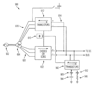
FIGURE 9 is a schematic illustrating an exemplary DC bus regulator using a
resistor and capacitor for reverse power regulation according to one
embodiment of the
invention. Regulator 900 accepts input from AC source 602 after conditioning
by
transformer 604 into line 610 and line 620. Transistor pack 612 couples line
610 to DC
bus 614 and diode pack 822 couples line 620 to DC bus 614. An SCR pack could
be used
-16-
CA 02792807 2012-10-17
in place of diode pack 822 to achieve similar results. Additionally, switch
942 couples
capacitors 944 and resistors 946 to DC bus 614. Switch 942 may be controlled
by
microcontroller 613 to enable or disable capacitors 944. Additionally, switch
950 and
switch 952 coupled to capacitors 944 and resistors 946, respectively, allow
energy to be
stored in capacitors 944 or dissipated through resistors 946. In reverse power
operation
region 521 power may flow through transistor pack 612 back to AC source 602.
When the
power capacity of transistor pack 612 is reached, microcontroller 613 may
enable 942
allowing power to flow to capacitors 944. When operation returns to region
521,
microcontroller 613 may turn off switch 942 and power flow occurs only through
transistor pack 612. Regulator 900 may also use a combination of resistors and
capacitors
in place of capacitors 944. Further, any other energy dissipation or energy
storage
technology may be used in combination or as a substitution for capacitors 944
such as
rotating masses or batteries.
Although the present disclosure has described in detail using three-phase AC
sources, one skilled in the art may readily modify the disclosure in this
application to
operate on a two phase or other AC system, or from DC generators.
In the design of FIGURE 1 multiple AC-to-DC converters are required as are
multiple DC-to-AC converters and DC-to-DC converters. For example, motor 134
may
operate on AC power and therefore it is necessary to convert the power on the
DC bus
back to AC before it may be utilized by motor 134. One skilled in the art will
recognize
that DC-to-AC power conversion may be accomplished using similar components as
are
used for AC-to-DC power conversion. For example, transistor pack 612 as shown
in
FIGURE 6, FIGURE 7, FIGURE 8, and FIGURE 9 may be configured to perform DC-to-
AC conversion. Also, DC-to-DC power conversion may be accomplished using
similar
components as DC-to-AC and AC-to-DC power conversion.
In the different regions of operation exemplarily shown in FIGURE 5, as power
flow is diverted from transistors to diodes or SCRs, at least a portion of the
transistor pack
no longer in use may be switched from converting AC-to-DC power for the DC bus
to
convert DC-to-AC power for an attached load, energy storage device, or
resistor. Such a
configuration may reduce the number of transistors required for the power
system
-17-
CA 02792807 2012-10-17
illustrated in FIGURE 1 thereby reducing the space requirements and the cost
of the
overall power system.
FIGURE 10 is a block diagram illustrating a swing pack for AC-to-DC, DC-to-AC,
and DC-to-DC conversion according to one embodiment of the invention. Power
system
1000 includes bank of converters 1002. Bank of converters 1002 may be any
number or
combination of devices capable of AC-to-DC, DC-to-AC, and DC-to-DC conversion,
such
as transistor pack 400 illustrated in FIGURE 4. Bank of converters 1002 are
coupled on
one side to DC bus 1020 and on another side to isolators 1004. Isolators 1004
when
closed couple one converter of bank 1002 to line 1014 leading to AC or DC
generators or
to line 1012 leading to AC or DC loads. The isolators may be controlled, for
example, by
a microcontroller or other control system that may be separate or the same as
microcontroller 613. Inductor 1006 conditions power before reaching line 1012
or line
1014. The selection of which power consumption units are engaged in generator
to DC
bus power transfer or DC bus to load may be based on the process at hand. For
example,
use of on power pack of bank 1002 to pass power to an energy storage device
would be
done when the DC bus had excess power and therefore the power pack would not
need to
be engaged in moving power from the generator to the DC bus.
Although the present disclosure and its advantages have been described in
detail, it
should be understood that various changes, substitutions and alterations can
be made
herein without departing from the spirit and scope of the disclosure as
defined by the
appended claims. Moreover, the scope of the present application is not
intended to be
limited to the particular embodiments of the process, machine, manufacture,
composition
of matter, means, methods and steps described in the specification. As one of
ordinary
skill in the art will readily appreciate from the present invention,
disclosure, machines,
manufacture, compositions of matter, means, methods, or steps, presently
existing or later
to be developed that perform substantially the same function or achieve
substantially the
same result as the corresponding embodiments described herein may be utilized
according
to the present disclosure. Accordingly, the appended claims are intended to
include within
their scope such processes, machines, manufacture, compositions of matter,
means,
methods, or steps.
-18-