Note: Descriptions are shown in the official language in which they were submitted.
CA 02793788 2012-09-19
1
Specification:
Method for purifying silicon
Technical Field
The present invention refers to a method for manufacturing high-purity
silicon. The manufactured silicon is used for solar cells.
Background Art
Photovoltaic power generation is a technology converting light power
directly into electrical power by using the photovoltaic effect of
semiconductor interfaces. The key components of this technology are
solar cells, and one of the key factors of manufacturing solar cells is
the preparation of high purity silicon.
In order to lower the cost of the photovoltaic power generation and
promote the transformation of the photovoltaic power generation into a
principal energy, it is a strategic measure to avoid the modified
Siemens process in the prior art which is high-cost, high-energy-
consumption and environmental burden, and to seek new purification
methods for manufacturing high purity silicon used in solar cells which
are low-cost, low-energy-consumption and environment-friendly.
Generally, the metallurgy method (physical method) which has
achieved initial success is a combination of two types of purification
processes. The first type, the basic processes included in the physic
method, are the directional solidification and the zone-melting which
are able to remove the majority of impurities from silicon and enhance
the overall purity of silicon. The second type is a purification process
CA 02793788 2012-09-19
2
specially for removing electrically active impurities in silicon such as
boron and phosphor which are difficult to be removed by the first type.
The combination of these two types has produced high purity silicon
which can be used in the preparation of solar cells. The actual result
shows however that the prepared solar cells have the defects: the
photoelectric conversion efficiency is insufficient and deteriorates
rapidly. This indicates that the content of impurities in the high purity
silicon prepared by the prior art methods is still unstable and the purity
of silicon needs to be further improved. Therefore, the metallurgy
method in prior art is still unable to meet the requirement of solar
cells.
The principle of employing the directional solidification and the
zone-melting for purification and impurity removal is based on the
segregation effect of impurities while silicon being in. the state of
solid-liquid double-phase equilibrium. The said segregation effect
means that the concentrations of impurities in solid state and liquid
state are different. Csoiid represents the concentration of impurities in
solid state of silicon, CLiquid represents the concentration of impurities
in liquid state, and K indicates the segregation effect of impurities.
Thus, K=Csoiid /CLiquid. This formula is determined by the
thermodynamic characteristics when impurities and silicon are of
solid-liquid double-phase equilibrium and represents a physical
phenomenon ubiquitous in nature.
The directional solidification and the zone-melting , with the help of
the segregation effect of impurities, make silicon to be purified into
ingots, and further make the ingots (whole ingot or one portion) melt,
and control the solid-liquid interface to shift from the head of the ingot
CA 02793788 2012-09-19
3
to the foot of it. As the K value of the overwhelming majority of
impurities in silicon is less than 1 and the concentration of impurities
in solid state is far below that in liquid state, impurities in silicon are
redistributed during the process of solid-liquid interface shifting from
head to foot. The impurities discharged continuously from the
solidified solid phase to the liquid phase are brought to the part that
solidifies later, until they arrive at the foot part by the liquid-phase
silicon that has not solidified yet. Finally, the purified high purity
silicon is obtained by cutting off the impurity-enriched foot part. As
one of the basic methods for purification, the directional solidification
and zone-melting have also been used widely for the purification of
more materials besides silicon
The distribution of impurities along the length of an ingot after the
directional solidification is illustrated in fig.1. Regarding the impurities
wherein K<1, with the shift of solid-liquid interface from the head to
foot of an ingot, the impurities discharged from the solid phase
accumulate on the solid-liquid interface. Consequently, the
concentration on the liquid-phase side of the interface increases,
which also results in the increase of the concentration of impurities in
the solid phase at the time of crystallization. In fig.1, curve a
indicates the result of impurities accumulated on the solid-liquid
interface shifting to melting silicon because of concentration diffusion.
Curve b indicates a limit state (ideal state) where the impurities
discharged from the solid phase spread swiftly to the liquid phase,
which makes the concentration of impurities reach a uniform state. By
taking measures to slow down the moving speed of the interface and
accelerate the spreading speed of impurities, the distribution of
CA 02793788 2012-09-19
4
impurities along the length of an ingot after solidification is between
the two curves a and b.
In the directional solidification and zone-melting, the solid-liquid
interface which has an effect on the segregation of impurity is always
equal to the cross-sectional area of an ingot. In that case, slowing
down the moving speed of the interface is the only way to enhance the
result of the segregation effect. It can be known from fig.1 that the
concentration of impurity decreases below the original concentration
Co and the length of ingot is less than half of the entire ingot after one
operation of directional solidification.
It is discovered after the analysis of the purification process of the
directional solidification and the zone-melting that in the process of
carrying out the impurity removal and purification by using the
segregation of impurity, there exist serious shortcoming defects such
as being low effect, time consuming, energy consuming and material
consuming. It is inappropriate to apply this conventional segregation
method to the purification of the industrial silicon as crude metal with
high impurity content.
Summary of the invention
The main object of the present invention is to provide a new method
for the purification of silicon, which, in comparison with the directional
solidification and zone-melting, can improve the efficiency of
purification remarkably and enhance the purity of the industrial silicon
high enough to meet the requirements of solar cells.
CA 02793788 2012-09-19
The present invention employs the following technical solutions in
order to achieve the. said object.
A method for the purification of silicon, comprises the steps of:
(1) adding melting Na2CO3 which accounts for 10% by weight into the
melting silicon to be purified, and then adding covering agent to the
surface of the melt blend after stirring for 10 minutes;
(2) starting to monitor and record the temperature of the silicon to be
purified;
(3) reducing the cooling speed when the temperature is lowered to
1490^- 1510 C (namely, 80^- 100 C higher than the melting point of
silicon)
(4) Keeping the heating power constant when the temperature
reduces to the melting point of silicon;
(5) stopping heating when silicon starts to cool down;
(6) cooling silicon naturally down to room temperature and taking out
the crystallized solid silicon;
(7) At room temperature, crushing the crystallized silicon and soaking
them in the mixed acid solution, subject to standing in a fume hood
for 12 hours; and
(8) separating the silicon grains fragmented by leaching from the acid
solution, adding water for soaking, rinsing with water till neutral,
filtering, drying, and high-purity silicon is obtained.
The above mentioned method for the purification of silicon,
characterized in that: the said covering agent is wheat straw or rice
straw and should be added in an amount to entirely cover the surface
of the silicon to be purified.
CA 02793788 2012-09-19
6
The said method for the purification of silicon, wherein, the said mixed
acid solution is one of HCL of 19% by weight, HNO3 of 49% by weight
or H2SO4 of 49% by weight, or any two or more than two of them with
equal weight.
The method for the purification of silicon using grain-boundary doping
effect, characterized in that the melting silicon to be purified is placed
in the temperature-controllable crystallizer, the number of silicon
crystal nucleus and the growing speed of the grains at the time of
solidification is adjusted, the segregation effect of impurities on the
surface of grains and the interface of melts is used to make the
impurities discharged from the grains to accumulate on the grain
boundary, and then the purified silicon is obtained by setting free the
grains of silicon wrapped by impurities.
The said adjustment of the number of silicon crystal nucleus at the
time of solidification refers to forming at the same time a large number
of crystal nucleus instantly, enlarging solid-liquid interface.
The said setting free the grains of silicon wrapped by impurities refers
to that the high-purity grains wrapped by impurities are set free when
the impurities on the grain boundary is soaked and dissolved by the
acid solution.
The impurities concentrating on the grain boundary separate out from
the grain boundary during the cooling process and form into isolated
impurity phase.
The said temperature-controllable crystallizer comprises the outer
temperature-controlling panel and the crystallizer placed inside. The
CA 02793788 2012-09-19
7
said temperature-controlling panel controls the temperature of silicon
melt during the process of crystallization by the built-in heating device.
The said crystallizer contains inside the temperature-controlling
thermocouple connected with program temperature controller.
The favorable effects of the present invention are as follows:
The present invention provides a brand-new method of purification
using the segregation effect of impurities, hereinafter referred to as
grain boundary doping method. The steps included are: adding the
melting industrial silicon specially-made and temperature controllable
crystallizer; adjusting the number of silicon crystal nucleus at the time
of solidification and the growing speed of the grains by macro means
in order to make full use of the segregation effect of impurities on the
surface of grains and the interface of melts; the impurities discharged
from the grains concentrate on the grain boundary that finally solidify.
Then the silicon with a higher purity is obtained by setting free the
grains of pure silicon wrapped by impurities by effective means.
Compared with the conventional directional solidification and
zone-melting, the present invention is superior in the following
aspects:
1. The segregation efficiency of impurities in the solidification process
has been greatly enhanced, which accordingly increases the efficiency
and effect of purification. According to the purification method of the
present invention, a large number of crystal nucleuses are instantly
formed at the same time, which produces big solid-liquid interface.
With the growth of crystal nucleuses of silicon, the growth of the area
of the solid-liquid interface is proportional to the second power of the
CA 02793788 2012-09-19
8
radius of grains, and therefore there will be obvious change in the
effect of segregation and purification.
2. The process of purification is greatly shortened. It can be known by
comparing the crystallization process of 10kg of industrial silicon
using grain boundary doping and the process of the directional
solidification using 10kg of silicon that: the average size of grains of
the industrial silicon is 1 millimeter after solidification in the
crystallizer. Supposing that it takes 30 minutes from the start of
crystallization to the entire solidification, then the growth speed of
grains (the advancing speed of the solid-liquid interface) is
1 millimeter/hour. Accordingly, it takes 530 hours (22 days) for 10kg of
silicon casted into a billet with a section of 9cmX9cm and a length of
53cm to finish the directional solidification at this speed. However,
according to the grain boundary doping method, a large number of
crystal nucleuses starts at the same time, each grain meets the other
one only after it extends by 1 millimeter towards the space around,
and impurities are removed to the grain boundary. This takes only 30
minutes.
3. The actual yield of pure materials is increased. A large number of
grains grow simultaneously in three-dimensional space and integrate
in the end. Due to the highly efficient segregation effect, the impurities
from silicon concentrate on the grain boundary that finally solidifies.
The impurities concentrating on the grain boundary separate out from
the grain boundary during the cooling process and form into isolated
impurity phase. The high-purity silicon grains wrapped by impurities
are set free when the impurities on the grain boundary are soaked and
dissolved using acid solutions. The purified silicon collected thereby
CA 02793788 2012-09-19
9
suffers a small loss and the actual yield is greatly enhanced compared
with the directional solidification that needs to cut off the tail part of
impurity repeatedly.
The grain boundary doping method shares the same theory as the
directional solidification and zone-melting in terms of the removal of
impurities, nevertheless, the segregation effect is particularly
remarkable. The purity quality of silicon after purification will be
effectively increased. Moreover, after further treatment of removing
boron and phosphorus, the requirements from solar cells for
high-purity silicon can be well met.
Brief Description of the Drawings
Fig.1 is a curve containing the concentration of impurities and
solidification part during the process of the directional solidification.
Fig.2 is a stepped cooling curve of the industrial silicon during the
cooling process.
Fig.3 is the external front view of the temperature-controllable
crystallizer used in the method of purification of the present invention.
Fig.4 is the external left view of the temperature-controllable
crystallizer used in the method of purification of the present invention.
Fig.5 is the external right view of the temperature-controllable
crystallizer used in the method of purification of the present invention.
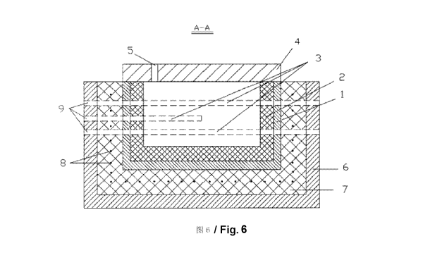
Fig.6 is the A-A section view of fig.4.
Fig.7 is the B-B section view of fig.3.
CA 02793788 2012-09-19
Detailed description of the preferred embodiments
The exterior and structure of the typical temperature-controllable
crystallizer for conducting the grain boundary doping method of the
present invention is illustrated in fig.3-fig.7.
The said temperature-controllable crystallizer comprises the outer
temperature-controlling panel and the crystallizer inside the said
panel. The said crystallizer has a double-layer structure including
case 1 made from the heat-resisting metal and lining 2 made from
flame-resisting material. Five high-heat resistant alloy tubes 3 are
welded to the inner layer of the case 1, two of them on one side and
the other three on the other side. Among three alloy tubes on the same
side, the length of the alloy tube in the middle is half of the other 4
alloy tubes. This alloy tube forms a covered end on the inner layer of
case 1 close to the center of the crystallizer and the other end pass
through the crystallizer, which forms the opening to the outside. The
two ends of all the other 4 alloy tubes pass through the crystallizer,
forming the openings to the outside on the outer layer of case 1 . To
prevent heat radiation, the upper cap 4 made from flame resistant and
heat insulating material is installed above the crystallizer and a
prepared hole 5 is on the upper cap 4.
The said temperature-controlling panel also has a double-layer
structure including the case 6 made from heat resistant metal and the
lining 7 made from thermal insulating material. Plurality of heating
devices 8 are installed inside the said lining 7. The said case 6 and
lining 7 have plurality of 'through holes 9 on them. The said through
holes 9 are connected correspondingly with the openings of the alloy
tubes 3 on the case 1 of the crystallizer respectively.
CA 02793788 2012-09-19
11
The crystallizer is placed inside the lining 7 of the
temperature-controlling panel and thermal couples are inserted in 5
alloy tubes 3 via the through holes 9 on the temperature-controlling
panel. The temperature-controlling thermal couple is inserted in the
shorter alloy tube and is fixed to the position close to the center of the
crystallizer by the covered end of the said alloy tube. The thermal
couple of the upper cap is inserted inside the crystallizer via the
prepared hole 5 of the upper cap 4. The temperature output by each
thermal couple is monitored, the temperature-controlling couple is
linked to the program temperature-controller (not illustrated in the fig),
then the heating device 8 contained in the temperature-controlling
panel is adjusted, and thus the temperature of the silicon melt during
the crystallization process is controlled. The thermal couples inside
other 4 alloy tubes are movable in order to monitor the uniformity of
the temperature during the crystallization process inside the
crystallizer.
The melt of the industrial silicon is added to the crystallizer whose
temperature can be controlled by program. It can be known according
to the cooling curve of the industrial silicon during the cooling process
illustrated in fig.2 that: point A is the temperature of the silicon melt at
the time of entry into the crystallizer. With the heat radiation of the
melt, the temperature declines gradually. A large number of crystal
nucleuses inside the melt start to form and grow while reaching point B
and silicon melt starts to be in a state of solid-liquid two-phase
equilibrium. Due to the release of solid-phase latent heat, the
temperature of the silicon melt remains unchanged in the state of
two-phase equilibrium, constant at 141 0 C . During the growth process
CA 02793788 2012-09-19
12
of crystal nucleuses, segregation happens to impurities. Silicon grains
grow freely in the volume space of the crystallizer and the surface of
grains is solid-liquid interface of two-phase equilibrium. With the
growth of grains, the area of the interface extends, proportional to the
second power of the radius of grains. Impurities, however, are
removed to the melting silicon that has not yet solidified and finally
concentrate on the grain boundary of grains. The melting silicon on
the grain boundary gather impurities (the impurities of K < 1)
discharged from grains. The curve C is reached when all silicon melt
solidifies. At this point, there is no more release of solid-phase latent
heat. From then on, the temperature continues to decline and
impurities separate out on the grain boundary one after another. The
solidified silicon is taken out from the crystallizer, added to the acid
tub after being crushed properly, and then soaked for 12 hours in the
mixed acid solution. The acid solution infiltrates along the grain
boundary. The grain boundary breaks after impurities are dissolved,
and thus silicon grains after purification are set free. The silicon
grains are rinsed by purified water to be neutral after being separated
from the acid solution. The high-purity silicon is obtained after drying.
Examples
(1) Adding the melting silicon to the crystallizer that has been already
placed in the temperature-controlling panel, adding therein the
melting Na2CO3 which accounts for 10% by weight of the silicon to
be purified, and after stirring for 10 minutes, adding the wheat
straw as covering agent to its surface, and then covering the upper
cap 4;
(2) Inserting the thermal couple of the upper cap in the prepared
holes 5 of the upper cap and starting the temperature recorder.
CA 02793788 2012-09-19
13
(3) Starting the heating device 8 in the temperature-controlling panel
to reduce the cooling speed when the temperature is lowered to
about 1500 C;
(4) Lifting the thermal couple of the upper cap and sealing the
prepared holes 5 when the temperature cools down to the melting
point of silicon. Keeping the heating power of the
temperature-controlling panel constant. Recording the difference
between the temperature indicated by the fixed
temperature-controlling couple of the tube in the middle and the
upper-cap couple, and from then on, the crystallization process is
judged from the temperature indicated by the fixed
temperature-controlling thermal couple and the temperature is
printed out continuously by the temperature recorder;
(5) When the temperature curve shows the turning point meaning the
start of cooling down, it indicates that the crystallization is finished
and therefore heating is stopped.
(6) The solid silicon is taken out from the crystallizer when the
temperature cools down to room temperature.
(7) At room temperature, silicon is crushed and soaked in the acid tub
wherein the mixed acid solution containing 19% by weight of HNO3
and 49% by weight of H2SO4 in a 1:1 (by weight) proportion is
added. Silicon fragments are soaked and subject to standing in a
fume hood for 12 hours.
(8) Silicon grains fragmented by leaching are separated from the acid
solution, adding water for soaking, rinsing with water till neutral,
filtering, and drying, and high-purity silicon is thus obtained.