Note: Descriptions are shown in the official language in which they were submitted.
I 2-0&20
WO 2011/127557 PCT/CA2011/000329
1 1337-03PCT-000-00
PHASE CHANGE MEMORY WITH DOUBLE WRITE DRIVERS
CROSS-REFERENCE TO RELATED APPLICATIONS
This application claims priority from U.S. Provisional
Patent Application Ser. No. 61/323,396 filed on 13 April,
2010 and US 13/073,041 filed March 28, 2011 (Pyeon) for
"PHASE CHANGE MEMORY WITH DOUBLE WRITE DRIVERS", the entire
contents of which are incorporated herein by reference.
FIELD OF THE INVENTION
The present invention relates generally to Phase Change
Memory (PCM) and more specifically to a PCM having double
write drivers.
BACKGROUND
Conventional Phase Change Memory (PCM) devices store data
using phase change materials, such as chalcogenide, which
are capable of stably transitioning between amorphous and
crystalline phases. The amorphous and crystalline phases
(or states) exhibit different resistance values used to
distinguish different logic states of memory cells in the
memory devices. In particular, the amorphous phase exhibits
a relatively high resistance and the crystalline phase
exhibits a relatively low resistance.
At least one type of phase change memory device-PRAM-uses
the amorphous state to represent a logical 11' and the
crystalline state to represent a logical `0'. In a PRAM
device, the crystalline state is referred to as a "set
state" and the amorphous state is referred to as a "reset
state". Accordingly, a memory cell in a PRAM stores a
logical 10' by setting a phase change material in the
I 2-0&20
WO 2011/127557 PCT/CA2011/000329
2 1337-03PCT-000-00
memory cell to the crystalline state, and the memory cell
stores a logical `1' by setting the phase change material
to the amorphous state.
The phase change material in a PRAM is converted to the
amorphous state by heating the material to a first
temperature above a predetermined melting temperature and
then quickly cooling the material. The phase change
material is converted to the crystalline state by heating
the material at a second temperature lower than the melting
temperature but above a crystallizing temperature for a
sustained period of time. Accordingly, data is programmed
to memory cells in a PRAM by converting the phase change
material in memory cells of the PRAM between the amorphous
and crystalline states using heating and cooling as
described above.
The phase change material in a PRAM typically comprises a
compound including germanium (Ge), antimony (Sb), and
tellurium (Te), i.e., a "GST" compound. The GST compound is
well suited for a PRAM because it can quickly transition
between the amorphous and crystalline states by heating and
cooling. In addition to, or as an alternative for the GST
compound, a variety of other compounds can be used in the
phase change material. Examples of the other compounds
include, but are not limited to, 2-element compounds such
as GaSb, InSb, InSe, Sb2Te3, and GeTe, 3-element compounds
such as GeSbTe, GaSeTe, InSbTe, SnSb2Te4, and InSbGe, or 4-
element compounds such as AgInSbTe, (GeSn)SbTe, GeSb(SeTe),
and Te81 Ge15Sb2S2.
The memory cells in a PRAM are called "phase change memory
cells". A phase change memory cell typically comprises a
I 2-0&20
WO 2011/127557 PCT/CA2011/000329
3 1337-03PCT-000-00
top electrode, a phase change material layer, a bottom
electrode contact, a bottom electrode, and an access
transistor. A read operation is performed on the phase
change memory cell by measuring the resistance of the phase
change material layer, and a program operation is performed
on the phase change memory cell by heating and cooling the
phase change material layer as described above.
Fig. 1 is a schematic circuit diagram illustrating a
conventional Phase Change Memory (PCM) cell with MOS 10 and
a conventional diode PCM cell 20. Referring to Fig. 1,
memory cell 10 includes a phase change resistance element
11 comprising the GST compound, and a negative metal-oxide
semiconductor (NMOS) transistor 12. Phase change resistance
element 11 is connected between a bit line BL and NMOS
transistor 12, and NMOS transistor 12 is connected between
phase change resistance element 11 and ground. In addition,
NMOS transistor 12 has a gate connected to a word line WL.
NMOS transistor 12 is turned on in response to a word line
voltage applied to word line WL. Where NMOS transistor 12
is turned on, phase change resistance element 11 receives a
current through bit line BL.
Referring to Fig. 1, memory cell 20 comprises a phase
change resistance element 21 connected to a bitline BL, and
a diode 22 connected between phase change resistance
element 21 and a wordline WL.
Phase change memory cell 20 is accessed by selecting
wordline WL and bitline BL. In order for phase change
memory cell 20 to work properly, wordline WL preferably has
a lower voltage level than bitline BL when wordline WL is
I 2-0&20
WO 2011/127557 PCT/CA2011/000329
4 133'/- U_3Yu'1'-uuu-u0
selected so that current can flow through phase change
resistance element 21. Diode 22 is forward biased so that
if wordline WL has a higher voltage than bitline BL, no
current flows through phase change resistance element 21.
To ensure that wordline WL has a lower voltage level than
bitline BL, wordline WL is generally connected to ground
when selected.
In Fig. 1, phase change resistance elements 11 and 21 can
alternatively be broadly referred to as "memory elements"
and NMOS transistor 12 and diode 22 can alternatively be
broadly referred to as "select elements".
The operation of phase change memory cells 10 and 20 is
described below with reference to Fig. 2. In particular,
Fig. 2 is a graph illustrating temperature characteristics
of phase change resistance elements 11 and 21 during
programming operations of memory cells 10 and 20. In Fig.
2, a reference numeral 1 denotes temperature
characteristics of phase change resistance elements 11 and
21 during a transition to the amorphous state, and a
reference numeral 2 denotes temperature characteristics of
phase change resistance elements 11 and 21 during a
transition to the crystalline state.
Referring to Fig. 2, in a transition to the amorphous
state, a current is applied to the GST compound in phase
change resistance elements 11 and 21 for a duration T1 to
increase the temperature of the GST compound above a
melting temperature Tm. After duration T1, the temperature
of the GST compound is rapidly decreased, or "quenched",
and the GST compound assumes the amorphous state. On the
other hand, in a transition to the crystalline state, a
I 2-0&20
WO 2011/127557 PCT/CA2011/000329
1337-03PCT-UUU-UO
current is applied to the GST compound in phase change
resistance elements 11 and 21 for an interval T2 (T2>Tl) to
increase the temperature of the GST compound above a
crystallization temperature Tx (Tx 2, the GST compound is
slowly cooled down below the crystallization temperature so
that it assumes the crystalline state.
A phase change memory device typically comprises a
plurality of phase change memory cells arranged in a memory
cell array. Within the memory cell array, each of the
memory cells is typically connected to a corresponding bit
line and a corresponding word line. For example, the memory
cell array may comprise bit lines arranged in columns and
word lines arranged in rows, with a phase change memory
cell located near each intersection between a column and a
row.
Typically, a row of phase change memory cells connected to
a particular word line are selected by applying an
appropriate voltage level to the particular word line. For
example, to select a row of phase change memory cells
similar to phase change memory cell 10 illustrated in the
left side of Fig. 1, a relatively high voltage level is
applied to a corresponding word line WL to turn on NMOS
transistor 12. Alternatively, to select a row of phase
change memory cells similar to phase change memory cell 20
illustrated in the right side of Fig. 1, a relatively low
voltage level is applied to a corresponding word line WL so
that current can flow through diode 22.
The SLC (single level) cell with PCM has a lot of sensing
margin between logic 11' (amorphous, reset state) and logic
`0' (`crystalline, set state) due to the resistive
I 2-0&20
WO 2011/127557 PCT/CA2011/000329
6 1337-03PCT-000-00
difference almost 10 to 100 times. However, in case of MLC
(Multiple Level Cell), the distinguishing difference
between two logic states would not be continued. As well,
the Phase change memory density has increased drastically
so that the near cell and far cell writing characteristics
is one of issues to be resolved.
In United States patent 7,110,286, "PHASE-CHANGE MEMORY
DEVICE AND METHOD OF WRITING A PHASE-CHANGE MEMORY DEVICE",
to Choi et al., issued 9/19/2006 (hereinafter, Choi) and
incorporated herein by reference, there is disclosed a
different pulse control depending on the row addresses to
compensate the cell resistance variation induced by a bit
line parasitic resistive factor. Choi can resolve the cell
set and reset resistance variation, but it needs more
complicated control with row address inputs. Also, its
variation difference is changed depending on the process
condition and process technologies.
Accordingly, there is a need for the development of an
improved apparatus, method, and system using PCM as well as
non-volatile memory devices and systems utilizing such
improved PCM.
SUMMARY
It is an object of the present invention to provide an
apparatus, method, and system using Phase Change Memory
(PCM) having reduced effects of high write current.
According to one aspect of the invention the is provided an
apparatus including a memory array having a bitline with a
first end and a second end for accessing a PCM cell coupled
to the bitline between the first end and the second end of
I 2-0&20
WO 2011/127557 PCT/CA2011/000329
7 1337-03PCT-000-00
the bitline, a first write driver and a second write driver
coupled to the first end of the bitline and the second end
of the bitline respectively for simultaneously supplying
current to the PCM cell when writing to the PCM cell; and a
sense amplifier coupled to the second end of the bitline
for sensing a resistance of the PCM cell when reading from
the PCM cell.
Beneficially, the first write driver and the second write
driver are coupled to the first end of the bitline and
second end of the bitline through a first column selector
and a second column selector respectively.
Beneficially, the memory array comprises a wordline coupled
to the PCM cell for selecting the PCM cell.
Alternatively, the wordline is coupled to the PCM cell by
an insulated-gate field effect transistor (IGFET) or a
diode.
Advantageously, the PCM cell is a Multiple Level Cell
(MLC).
According to another aspect of the invention there is
provided a method of writing data to a PCM cell including
supplying current to the PCM cell simultaneously from a
first write driver and a second write driver coupled to a
first end of a bitline and a second end of the bitline
respectively.
Beneficially, the method includes selecting the PCM cell
using a wordline.
I 2-0&20
WO 2011/127557 PCT/CA2011/000329
8 1337-03PCT-000-00
Beneficially, supplying current to the PCM cell
simultaneously from a first write driver and a second write
driver includes supplying current to the PCM cell
simultaneously from a first write driver through a first
column selector and a second write driver through a second
column selector
According to yet another aspect of the invention there is
provided a system including a Phase Change Memory (PCM)
apparatus having a memory array including a bitline having
a first end and a second end for accessing a PCM cell
coupled to the bitline between the first end and the second
end of the bitline, a first write driver and a second write
driver coupled to the first end of the bitline and the
second end of the bitline respectively for simultaneously
supplying current to the PCM cell when writing to the PCM
cell; and a sense amplifier coupled to the second end of
the bitline for sensing a resistance of the PCM cell when
reading from the PCM cell.
Preferably, the first write driver and the second write
driver are coupled to the first end of the bitline and
second end of the bitline through a first column selector
and a second column selector respectively.
Beneficially, the memory array comprises a wordline coupled
to the PCM cell for selecting the PCM cell.
Optionally, the wordline is coupled to the PCM cell by an
insulated-gate field effect transistor (IGFET) or a diode.
Preferably, the PCM cell is a Multiple Level Cell (MLC).
I 2-0&20
WO 2011/127557 PCT/CA2011/000329
9 1337-03PCT-000-00
Thus improved apparatuses, methods, and systems have been
provided.
BRIEF DESCRIPTION OF THE DRAWINGS
Further features and advantages of the present invention
will become apparent from the following detailed
description, taken in combination with the appended
drawings, in which:
Fig. 1 is a schematic diagram of a conventional NMOS switch
PCM (Phase Change Memory) cell and a conventional diode
switch PCM cell;
Fig. 2 is a graph of temperature change during a set and a
reset operation of a conventional PCM cell;
Fig. 3 is a schematic diagram of circuits in a cell array
of a conventional PCM device;
Fig. 4 is a schematic diagram of an equivalent circuit of a
bit line shown in Fig. 3;
Figs. 5A and 5B are distribution diagrams of data in
multilevel cells in PCM devices;
Fig. 6 is a block diagram of a first embodiment of a PCM
device in accordance with an example embodiment of the
invention;
Fig. 7A is a schematic diagram of circuits in a cell array
of the PCM device shown in Fig. 6;
Fig. 7B is a schematic diagram of an equivalent circuit of
a bit line shown in Fig. 7A;
I 2-0&20
WO 2011/127557 PCT/CA2011/000329
1337-03PCT-000-00
Figs. 8A and 8B are schematic diagrams of equivalent
circuits for voltage sensing and current sensing
respectively;
Fig. 9 is a block diagram of a second embodiment of a PCM
device in accordance with an example embodiment of the
invention;
Fig. 10 is a block diagram of a third embodiment of a PCM
device in accordance with an example embodiment of the
invention; and
Figs. 11A to 11C are diagrams of electric devices including
the memories shown in Figs. 6, 9, and 10 respectively.
It will be noted that throughout the appended drawings,
like features are identified by like reference numerals.
DETAILED DESCRIPTION OF EMBODIMENTS
As described herein above, the write current variation
caused by distance from the write driver to a destination
cell affects cell resistance distributions of Phase Change
Memory (PCM) cells and especially MLC (Multiple Level Cell)
PCM cells.
Fig. 3 is a schematic diagram of circuits in a cell array
302 of a conventional PCM device. The array includes a
plurality of PCM cells 304 arranged in rows selectable by
wordlines 306 and columns selectable by bitlines 308 and
column selectors 310. The arrow 314 indicates a path of
write current taken from a write driver 312 through a
selected cell 316 to ground.
I 2-0&20
WO 2011/127557 PCT/CA2011/000329
11 1337-03PCT-000-00
Referring to Fig. 4, there is shown schematically four
representative resistive factors from the write driver 312
to memory cell ground 412, there are:
Rsel: Column selector transistor channel resistance 402
Rbl: Parasitic bit line resistance 404
Rdiode: diode forward-bias resistance 408
Rgnd: Word line resistance (junction resistance) +
relevant MOS transistor channel resistance 410.
Unlike a DRAM bit line which has parasitic capacitance as
dominant power consumption factor and performance
degradation, the phase change memory needs very high write
current flowing through the direct current path between VDD
and V. Therefore, the resistive factor on bit lines is
more important than the capacitive one. In order to reduce
the parasitic resistance, one can increase the width or
height of bit line. However, it causes cell size due to the
wider bit line and low cell yield by topological
difficulty.
Referring to Fig 5A, there is shown a data distribution
diagram 500 of a 2 bits/cell multi-level cell (MLC) PCM
device. MLC implementation demands more precise control of
cell resistance distribution 501 for each logic value 502
to ensure read operation margins 504,506,508 among bit
definitions. When more bits are assigned into the single
cell, as in Fig. 5B where there is shown a data
distribution diagram 510 of a 3 bits/cell MLC PCM device
for each logic value 512, the read operation margins
514,516,518,520,522,524,526 are reduced.
I 2-0&20
WO 2011/127557 PCT/CA2011/000329
12 1337-03PC1'-UUU-00
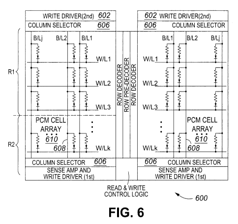
Referring to Fig. 6, there is shown a block diagram of a
PCM memory 600 including a first embodiment in accordance
with the present invention that provides two physically
separated write drivers 602,604 (also referred to herein as
double write drivers) at a top 602 and a bottom 604 end of
a PCM memory cell array 610. Preferably both write drivers
on the top 602 and bottom 604 sides drive simultaneously
write current to a same selected cell. The top and bottom
write (also referred to herein as first and second write
drivers respectively) drivers 602,604 are connected or
coupled electrically through the column selector 606 to the
same bit line 608. Note that the terms "top" and "bottom"
are used herein for convenience and clarity when referring
to the figures. The memory 600 may be oriented in any
position and be within the scope of the invention.
conventional row decoder 614 and row pre-decoder 614
control selection of the wordlines 306. Read/Write control
logic 612 controls operation of the row decoders 614, row
pre-decoders 616, column selectors 606, sense amps 604 and
write drivers 602
Placement of double write drivers 602,604 according to an
embodiment of the invention provides advantages of:
reduction of parasitic bit line resistance by maximum 50%
of Rbl, that is, the middle of phase change memory cell has
a distal position from the write drivers; and column
selector channel resistance effect can be suppressed by
equivalent write driver current from top and bottom sides
write drivers 602,604.
The read sense amplifier 604 is preferably placed at one
end of the bit line 608 unlike the double write drivers
I 2-0&20
WO 2011/127557 PCT/CA2011/000329
13 1337-03PUT-UUU-U0
602,604. Since the read sensing is preferably not done at
both sides at the same time and the read operation does not
need separate control. Other preferred embodiments will be
disclosed herein below showing a location of the read sense
amplifier.
Embodiments of the present invention effectively reduce the
parasitic bit line resistance and selector transistor
channel resistance. Fig. 7A shows the reduction effect of
two resistive factors on the bit line 608. Fig. 7B is a
schematic diagram of an equivalent circuit 710 of a bit
line 608 shown in Fig. 7A for a worst case cell, that is
the cell half way between the double write drivers 602,604.
Note the halving of the bitline resistance and column
selector channel resistance 712.
Referring to Figs. 8A and 8B, the current sensing method
800 is affected by Rparasitic 802 (bit line parasitic
resistance); the voltage sensing method 810 is not affected
by Rparasitic 802. Their relationships are derived from basic
equations of sensing values.
Current sensing 800:
I one = Vforce / (RGST reset + Rparasitic)
'zero = Vforce / (RGST set + Rparasitic)
'zero Lone (Current sensing margin) = V* (RGST reset - RGST set)
(RGST reset * RGST_set + R 2 parasitic +Rparasitic (RGST_reset +
RGST set )
Voltage sensing 810:
Vone = Iforce * (RGST reset + Rparasitic)
I 2-0&20
WO 2011/127557 PCT/CA2011/000329
14 1337-03PCT-000-00
Uzero = Iforce * (RGST set + Rparasitic)
Vone - Vzero (Voltage sensing margin) = Iforce * (RGST reset -
RGST set) ; Rparasitic is not included.
Other embodiments of the present invention can provide
smaller chip size in case of multiple memory arrays. The
shared sense amplifier and write drivers can be placed into
the center of memory array. For example, referring to Fig.
9, there is shown a block diagram 900 of a second
embodiment of the present invention. The sense amplifiers
and write drivers 902 are shared between top and bottom
memory arrays or more generally between adjacent memory
arrays. In a third embodiment shown in Fig. 10, only the
sense amplifiers 1002 are shared between top and bottom
memory arrays.
Advantageously, embodiments of the present invention
provide a double write driver configuration with two-side
placement (top and bottom of memory array) for same bit
line. Only one side of write driver has read sense
amplifier (top or bottom).
Embodiments of the present invention also provide better
read operation sensing margin along with narrow cell
resistance distribution for each logic state.
The center of memory array has the read sense amplifier
while the top and bottom sides of memory array have write
drivers.
Both sides of write drivers are simultaneously activated
for the same bit line.
I 2-0&20
WO 2011/127557 PCT/CA2011/000329
15 1337-03PCT-000-00
Any type of phase change memory (NMOS selector, bipolar,
and diode) can be applied to implement embodiments of the
present invention.
As described herein above the memory systems shown in Figs.
6, 9, and 10 may also be embedded, as shown in Figs. 11A,
11B, and 11C respectively, in an electric device 1100. The
electric device 1100 may be, for example, a memory stick, a
solid state disk (SSD), a laptop computer, a desktop
computer, a personal digital assistant (PDA), audio player,
or the like where the advantages of embodiments of the
present invention are especially beneficial.
The embodiments of the invention described above are
intended to be exemplary only. The scope of the invention
is therefore intended to be limited solely by the scope of
the appended claims.