Note: Descriptions are shown in the official language in which they were submitted.
CA 02794010 2012-08-20
WO 2011/101680 PCT/GB2011/050322
A Controller
The present invention relates to a controller and particularly, but not
exclusively to a
controller for controlling the optical output of at least one light emitting
diode.
The optical output from an LED will vary over its useful lifetime and as such
the
perception of the light output will also vary.
We have now devised a controller for controlling the optical output of at
least one light
emitting diode.
In accordance with the present invention as seen from a first aspect, there is
provided a
controller for controlling the optical output of at least one light emitting
diode,
the controller comprising a control unit and a power supply unit for supplying
power to
the at least one light emitting diode,
the control unit being arranged to receive as input, first and second signals
which are
representative of the operating characteristics of the at least one light
emitting diode,
and which is further arranged to control the power output from the power
supply unit to
the at least one light emitting diode in dependence of the first and second
signals,
wherein
the first signal is representative of the current within the at least one
light emitting diode
and the second signal is representative of the temperature of the at least one
light
emitting diode.
The provision of two feedback loops enables the control unit to monitor and
adjust the
optical output of the light emitting diode and to provide for an energy saving
lighting
system, without compromising the visual perception of the optical output.
Preferably, the control unit further receives as input a third signal which is
representative
of the time and a fourth signal which is representative of ambient lighting
conditions.
The third signal is preferably generated by a clock which is arranged to
monitor the time,
such as the time of day and/or month and/or year, for example. The fourth
signal is
preferably generated by a sensor which senses ambient lighting conditions.
CA 02794010 2012-08-20
WO 2011/101680 PCT/GB2011/050322
2
The controller is preferably arranged to control the optical output of a
plurality of light
emitting diodes.
The controller is preferably powered by an alternating current mains supply.
The power
unit preferably receives as input a rectified direct current supply which is
obtained from
the alternating current mains supply.
The power supply to the controller and the power unit is preferably first
regulated to
minimise any voltage spikes.
In accordance with the present invention as seen from a second aspect, there
is
provided an energy saver light emitting diode (LED) power supply system
composed and
realized as shown in the description with the elements represented in the
drawing with
the exposed automatic controls and features, comprising:
an overvoltage suppression section to cut the voltage transient peaks of the
AC grid; a
Graetz Schottky diode bridge for the efficient high voltage AC\DC conversion;
a ripple
filter to obtain a stable DC voltage; an high efficiency resonant DC/DC buck
converter for
an efficient DC\DC conversion; a power unit that regulates efficiently voltage
and current
on the LED module; a control unit to manage automatically the other sections
and to
performs protection and energy saving operations; a LED module to convert
efficiently
the electrical energy supplied by the power unit into light energy.
In accordance with the present invention as seen from a third aspect, there is
provided a
method of controlling the optical output of at least one light emitting diode,
the method
comprising the steps of:
providing electrical power to the at least one light emitting diode to cause
the light
emitting diode to produce an optical output;
generating a first signal which is representative of the current passing
through the at
least one light emitting diode;
generating a second signal which is representative of the temperature of the
at least one
light emitting diode;
adjusting the electrical power supply to the at least one light emitting diode
in
dependence of the first and second signals.
CA 02794010 2012-08-20
WO 2011/101680 PCT/GB2011/050322
3
In accordance with the present invention as seen from a fourth aspect, there
is provided
a lighting system comprising an array of light emitting diodes and at least
one controller
of the first or second aspect.
An embodiment of the present invention will now be described by way of example
only
and with reference to the accompanying drawing, which illustrates an
electronic circuit
comprising a controller according to the described embodiment of the present
invention.
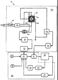
Referring to the drawing, there is illustrated an electronic circuit 10
comprising a
controller 20 for controlling the optical output of an array of light emitting
diodes (LED)
(not shown) housed within an LED module 30. The LED's are powered using a
power
unit 21 which receives as input a control signal from a control unit 22 and a
power supply
from a power modulation system 40.
The power modulation system 40 comprises a Graetz diode bridge 41 which
receives an
alternating current input from the mains 50, for example. The ac supply to the
diode
bridge 41 however, is first passed through a voltage suppression circuit 42
which is
arranged to remove any voltage spikes which appear from the mains 42 above a
threshold value, and a fuse 43, such as a self restoring fuse, which is
arranged to isolate
the power modulation system 40 from the mains 50 in the event that the mains
input
voltage far exceeds the average voltage.
The diode bridge 41 comprises four Schottky diodes 41a-d which are arranged to
minimize the voltage drop across the diode bridge 41, and thus minimize
electrical
power dissipation in the diode bridge 41.
The diode bridge 41 is arranged to generate a rectified voltage which is
subsequently
passed through a ripple filter 44 comprising a capacitor and resistor (not
shown)
arranged in a parallel configuration. The capacitors (not shown) of the filter
44 comprise
a low equivalent series resistance (ESR) to withstand any peaks in the
current, and
comprise a working temperature range which ensures a long filter lifetime. The
ripple
filter 44 is arranged to smooth the oscillating waveform from the diode bridge
41 and
CA 02794010 2012-08-20
WO 2011/101680 PCT/GB2011/050322
4
generate a substantially constant voltage, which is subsequently passed to a
buck
converter 45.
The buck converter is arranged to step-down the direct current voltage supply
from the
filter 44 to a useful voltage for powering the power unit 21 of the controller
20. The buck
converter 45 regulates the output voltage to the power unit 21 to produce a
stable,
constant voltage, and incorporates over-current protection, short-circuit
protection and
over-voltage protection circuitry to protect the power unit 21 from spurious
voltages from
the mains supply 50.
The power unit 21 is arranged to power the LED's of the LED module 30. The
power unit
21 is arranged to generate a low frequency pulse width modulation of the
voltage output
from the resonant converter 45, to modulate the energy to transfer to the LED
module
30. In order to minimise winding power losses associated with the converter
45, the
converter 45 operates without the mean value inductor-capacitor (L-C) filter
(not shown),
which is commonly used in buck converters, without affecting LED lifetime.
This is
because the LED's (not shown) of the module 30 are capable of withstanding the
peak
forward current surges.
The mean value of the voltage across the LED module 30 can be expressed as:
T
VM = T J V (t)dt
0
where V(t) is the impulse signal with variable duty cycle and with peak value
equal to the
output voltage of the buck converter 45.
The voltage output from the power unit 21 is controlled by a switch (not
shown), such as
a metal oxide semiconductor field effect transistor (MOSFET), which comprises
a low
drain-source resistance when arranged in the ON state. The switching frequency
of the
MOSFET (not shown) must be a maximum of 3-4 kHz to ensure a high efficiency
and to
reduce any voltage stresses on the LED's (not shown) of the module 30.
CA 02794010 2012-08-20
WO 2011/101680 PCT/GB2011/050322
The power modulation system 40 is also arranged to power the control unit 22.
The
output from the fuse 43 and the voltage suppression circuit 42 is passed
through a
current transformer 46 and then rectified and filtered using circuit 47 to
produce a
substantially stable uniform voltage. The output from the circuit 47 is
subsequently
5 passed to a voltage regulator 48 which further stabilizes the voltage supply
to the control
unit 22, such that the control unit 22 can maintain control of the entire
electronic circuit
and perform operations such as modifying the power supply to the buck
converter 45
and disabling a power factor correction of the buck converter 45 to increase
conversion
efficiency at low output current.
The control unit 22 comprises a microprocessor (not shown), or any other kind
of
programmable integrated circuit such as a field programmable gate array
(FPGA), which
is capable of controlling the power unit 21 in generating a pulse width
modulated (PWM)
signal. In this way the amount of power transferred to the LED module 30 is
proportional
to the duty cycle (D) of the PWM signal generated by the power unit 21. Upon
increasing
the duty cycle, more power will be delivered to the LED's (not shown) within
the module
30 per voltage period.
When the mean value of the output current is equal to the nominal value of LED
module
30 operating output current, the condition D < 1, must be satisfied. This is
because the
human eye is more sensitive to the peak of light intensity than the mean
value, while
power consumption is proportional to the mean value of the current absorbed.
In this
way, it is possible to obtain a better visual perception using less electrical
power.
The control unit 22 is arranged to set the duty cycle value following a
control algorithm
which has input values relating to the current within the LED's (not shown) of
the module
as determined by a current sensor 23, the temperature of the LED's (not shown)
as
determined by a temperature sensor 24, ambient light intensity as determined
by a light
sensor 25, and a time signal, such as the time of day and/or time of year, as
generated
30 by a clock 26.
The signal from the current sensor 23 is necessary for regulating the current
flow within
the LED's (not shown) and for short-circuit protection of the power unit 21.
The current
signal from the LED module 30, is further passed through a low pass filter 27
to generate
CA 02794010 2012-08-20
WO 2011/101680 PCT/GB2011/050322
6
an average current signal which is passed to the control unit 22. Accordingly,
when the
mean value of the current flowing in the LED module 30 deviates outside a pre-
defined
range, the control unit 22 is arranged to adjust the duty cycle applied to the
power unit
21 to vary the "ON" time during the voltage period and thus vary the current
which is
output therefrom.
When the mean value of the current flowing in the LED module 30 exceeds a
maximum
permitted current value for example, the control unit 22 is arranged to
generate a signal
which causes the power unit 21 to switch to the OFF state. The current sensor
23 is of
an electromagnetic inductive type to reduce losses associated with sensors
comprising
amperometric resistive shunts, thereby increasing the efficiency at which
electrical
power is converted to optical output from the LED's (not shown). The current
sensor 23
may comprise a transducer (not shown) comprising a wire winding formed on a
ferromagnetic ring (not shown), which must be crossed by one of the two wires
(not
shown) of the LED module 30.
The temperature sensor 24 which monitors the temperature of the LED's (not
shown), is
mounted on a circuit board (not shown) of the LED module 30 and is arranged to
generate a signal to the control unit 22 which is representative of the
temperature of the
circuit board (not shown), and thus the LED's (not shown). When the
temperature of the
LED module 30 deviates outside a pre-defined range, for example above 60 C,
the
control unit 22 decreases the duty cycle of the signal which is applied to the
power unit
21 in proportion to the deviation in the temperature of the LED's outside the
pre-defined
range, to vary the mean value of the current which is output from the power
unit 21, and
thus the temperature of the LED module 30. This kind of temperature control is
required
to extend LED lifetime and to make the LED's (not shown) operate near the
point of
maximum device efficiency. This is because LED luminous efficiency is
inversely
proportional to the temperature of the LED, and so by keeping this temperature
as low
as possible, the LED efficiency can be held at its maximum value.
When the temperature of the LED module 30 exceeds the maximum operating
temperature of the LED employed, the control unit 22 is arranged to generate a
signal
causing the power unit 21 to switch OFF the power supply to the module 30, and
thus
protect the LED's (not shown).
CA 02794010 2012-08-20
WO 2011/101680 PCT/GB2011/050322
7
The light sensor signal is required when, for example, there is a need to
lower the output
light intensity of the LED module 30, thereby saving an additional amount of
energy. The
output from the light sensor 25 may be sensitive to an external command, such
as a
remote control signal or a signal from a resistive potentiometer or a trimmer
(not shown),
for example. The signal from the light sensor 25 may be a binary serial signal
or an
analogue signal which is sampled by the control unit 22. The signal from the
light sensor
25 comprises information relating to the variation in duty cycle of the PWM
signal which
is required to realise the reduction in electrical power supply to the module
30.
The real time clock 26 is arranged to monitor the current time and is arranged
to deliver
time and day information to the control unit 22, so as to affect the light
output in
accordance with the time of day for example. The clock 26 is powered by a
battery (not
shown) and generates a serial signal with an interface protocol which is
recognized by
the control unit 22, such that the control unit 22 can provide for a gradual
or stepped
change in output light intensity.
The LED's (not shown) within the LED module 30 are arranged in an electrical
parallel
arrangement of rows of LED's (not shown), with the LED's (not shown) of each
row
being arranged in an electrical series configuration. The number of LED's (not
shown) in
series in each row must be more than ten, to reduce power losses due to
electrical
Ohmic conduction and to improve the efficiency of the buck converter 45. This
is
because the converter 45 provides an increased efficiency when the output
voltage is
higher and the output current is lower.
The LED module 30 comprises a further row comprising a series arrangement of a
resistor (not shown) and a Zener diode (not shown). The row comprising the
resistor
(not shown) and the Zener diode (not shown) is arranged in parallel to the
rows of LED's
(not shown) and must be connected such that the cathode of the Zener diode
(not
shown) is coupled to the anode of the LED (not shown). This scheme is helpful
as a
passive over-voltage LED protection circuit, but is essential, when one or
more LED's of
a series is interrupted or defectively soldered, for example.