Note: Descriptions are shown in the official language in which they were submitted.
CA 02795395 2012-10-02
- 1 -
Description
Production of monocrystalline semiconductor materials
[0001] The present invention relates to a method for
producing monocrystalline semiconductor materials, in
particular monocrystalline silicon. Furthermore, the
present invention relates to an installation for
producing such monocrystalline semiconductor materials.
[0002] Elemental silicon is used in different degrees
of purity inter alia in photovoltaics (solar cells) and
in microelectronics (semiconductors, computer chips).
Accordingly, it is customary to classify elemental
silicon on the basis of its degree of purity. A
distinction is made between, for example, "electronic
grade silicon" having a proportion of impurities in the
PPT range and "solar grade silicon", which is permitted
to have a somewhat higher proportion of impurities.
[0003] In the production of solar grade silicon and
electronic grade silicon, metallurgical silicon (in
general 98-99% purity) is always taken as a basis and
is purified by means of a multistage, complex method.
Thus, it is possible, for example, to convert the
metallurgical silicon to trichlorosilane in a fluidized
bed reactor using hydrogen chloride, said
trichlorosilane subsequently being disproportionated to
form silicon tetrachloride and monosilane. The latter
can be thermally decomposed into its elemental
constituents silicon and hydrogen. A corresponding
method sequence is described in WO 2009/121558, for
example.
[0004] The silicon obtained in this way quite
generally has at least a sufficiently high purity to be
classified as solar grade silicon. Even higher purities
can be obtained, if appropriate, by means of downstream
additional purification steps. At the same time, for
CA 02795395 2012-10-02
- 2 -
many applications it is favourable Or even
necessary for the silicon which emerges from the above
method and is generally obtained in polycrystalline
form to be converted into monocrystalline silicon.
Thus, solar cells composed of monocrystalline silicon
have a generally significantly higher efficiency than
solar cells composed of polycrystalline silicon.
[0005] The conversion of polycrystalline silicon into
monocrystalline silicon is generally effected by
melting of the polycrystalline silicon and subsequent
crystallization in a monocrystalline structure with the
aid of a seed crystal.
[0006] One technique for producing monocrystalline
silicon which makes it possible to produce silicon
single crystals having a particularly high degree of
purity is the so-called float zone method (FZ), which
was first proposed by Keck and Golay. An embodiment of
an FZ method and a device suitable for such a method
are presented e.g. in EP 1595006 Bl.
[0007] The FZ technique affords some significant
advantages over alternative methods such as the known
Czochralski method, for example, in particular as far
as the purity of the monocrystalline silicon obtained
is concerned. This is because in an FZ method the
silicon melt used for crystal growth is not held in a
crucible. Instead, the lower end of a rod composed of
polysilicon is lowered into the heating region of an
induction heating system and carefully melted. A melt
composed of molten silicon accumulates below the
silicon rod, a seed crystal composed of monocrystalline
silicon being dipped into said melt, generally from
below. As soon as the seed crystal is wetted with the
silicon melt, the crystal growth can be started by the
silicon melt being slowly lowered from the heating
zone. The silicon rod to be melted must be repositioned
from above at the same time, such that the volume of
- 3 -
the melt remains substantially constant. In the course
of the lowering of the melt, at the underside thereof a
solidification front forms along which the liquid
silicon crystallizes in the desired structure.
[0008] The production of monocrystalline silicon
proceeding from metallurgical silicon involves a very
high expenditure of energy. It is characterized by a
complex sequence of chemical processes and changes in
state of matter. In this connection, reference is made,
for example, to WO 2009/121558 already mentioned. The
silicon obtained in the multistage process described
therein is obtained in a pyrolysis reactor in the form
of solid rods which, if appropriate, have to he
comminuted and melted again for subsequent further
processing, for example in a Czochralski method or an
FZ method.
[0009] The present invention was based on the object
of providing a new technique for producing
monocrystalline silicon which is distinguished, in
particular, by a simplified method sequence and also by
energetic optimization relative to method sequences
known from the prior art.
[0010] In accordance with one embodiment of the
present invention, there is provided a method for
producing a monocrystalline semiconductor material
comprising the steps of: providing a starting material
composed of the semiconductor material, transferring
the starting material into a heating zone, in which a
melt composed of the semiconductor material is fed with
the starting material and lowering the melt from the
heating zone and/or raising the heating zone, such
that, at the lower end of the melt, a solidification
front forms along which the semiconductor material
crystallizes in the desired structure, wherein the
starting material composed of the semiconductor
material is provided in liquid form and fed into the
melt in liquid form, wherein for providing the liquid
starting material, particles of the semiconductor
material and/or a precursor compound of the
CA 2795395 2017-07-24
- 3a -
semiconductor material are fed into a gas flow, wherein
the gas flow has a sufficiently high temperature to
convert the particles of the semiconductor material
from the solid to the liquid and/or gaseous state
and/or to thermally decompose the precursor compound,
wherein the gas flow is conducted into a reactor
container, in which the liquid starting material is
condensed and/or separated from the gas flow, wherein
the reactor has a solid bottom region which at least
partly consists of the semiconductor material to be
produced, wherein the liquid starting material is fed
directly from the reactor container into the melt by
melting the bottom region in a controlled manner,
wherein the melting of the bottom region is controlled
by heating and/or cooling means which are arranged in
the bottom region or are assigned thereto, and wherein
the heating and/or cooling means comprise at least one
induction heating system and/or a focusable light beam
and/or beam of matter.
[0010a] In accordance with another embodiment of the
present invention, there is provided an installation
for producing a monocrystalline semiconductor material
comprising a source of a liquid semiconductor material
serving as starting material for the semiconductor
material, a reactor container comprising a heating
and/or cooling means for producing and/or maintaining a
melt composed of the semiconductor material in a bottom
region of the reactor container, and feeding means for
the liquid semiconductor material from the source to
the reactor container, the heating and/or cooling means
for at least partly melting the semi-conductor material
in the bottom region in a controlled manner, wherein
the heating and/or cooling means are arranged in the
bottom region of the reactor container or are at least
assigned thereto and comprise at least one induction
heating system and/or at least a focusable light beam
and/or a beam of matter.
CA 2795395 2017-07-24
- 4 -
[0011] By means of a method according to the
invention, it is possible, in principle, to obtain a
wide variety of semiconductor materials in
monocrystalline form. In particular, a method according
to the invention is suitable for producing
monocrystalline silicon. In this case, it always
comprises at least the following steps:
[0012] 1. In one step, a semiconductor material is
provided as starting material. The semiconductor
material is preferably silicon.
[0013] 2. In a further step, the starting material is
transferred into a heating zone. A melt composed of the
semiconductor material is situated in said heating
zone, said melt being fed with starting material. The
melt is a "freely floating melt" as in traditional FZ
methods, e.g. the method described in EP 1595006 Bl.
This should be understood to mean a melt which is not
in contact with the walls of a vessel such as a
crucible. Instead, its stability is maintained in a
contactless manner, which will be discussed in greater
detail below.
[0014] 3. By lowering the melt from the heating zone
or alternatively by raising the heating zone, it is
possible to bring about the formation of a
solidification front at the lower end of the melt,
along which the semiconductor material solidifies in
the desired monocrystalline structure. In principle,
the lowering of the melt from the heating zone and the
abovementioned raising of the heating zone can also be
effected simultaneously.
[0015] The method according to the invention is
particularly distinguished by the fact that the
starting material composed of the semiconductor
material is provided in liquid form and is also fed
into the melt in liquid form.
CA 2795395 2017-07-24
- 5 -
[0016] The method according to the invention thus has
some commonalities with traditional FZ methods, in
particular the "freely floating melt" mentioned. The
maintenance and stabilization of the melt and also the
cooling of the melt, in particular by lowering the melt
from the heating region, can be effected, in principle,
in accordance with procedures known from the prior art,
as mentioned and described e.g. in EP 1595006 El. In
contrast to traditional FZ methods, however, the melt
is not fed by repositioning a solid semiconductor
material, in particular a solid silicon rod as
mentioned in the introduction. Instead, the melt is fed
with starting material which is not first melted
directly above the melt, but rather is already in
liquefied form.
[0017] In order to form the desired monocrystalline
structure, the melt is seeded preferably with a seed
composed of a monocrystalline semiconductor material,
in particular a seed composed of monocrystalline
silicon, which can be dipped into the melt, in
particular from below. The melt correspondingly
solidifies during cooling along the solidification
front at its lower end in a monocrystalline structure.
[0018] The as yet unpublished German patent
application in the name of the present applicant with
the file reference DE 102010011853.2 and the
international application published as WO 2010/060630
with the file reference PCT/EP2009/008457 each describe
methods for obtaining silicon wherein silicon is
obtained in liquid form. The invention described in the
present case is based on these methods.
[0019] For providing the liquid starting material, in
preferred embodiments, particles of the semiconductor
material and/or a precursor compound of the
CA 2795395 2017-07-24
ak 02795395 2012-10-02
- 6 -
semiconductor material are fed into a gas flow,
as described in the two patent applications cited. If
appropriate, both particles of the semiconductor
material and a precursor compound of the semiconductor
material can be fed into the gas flow. The gas flow has
a sufficiently high temperature to convert the
particles of the semiconductor material from the solid
to the liquid and/or gaseous state and/or to thermally
decompose the precursor compound.
[0020] The precursor compound of the semiconductor
material could, in principle, also be heated directly,
such that thermal decomposition of the precursor
compound occurs, for example by energy being fed
thereto by means of electrostatic or electromagnetic
fields in order to convert it into a plasma-like state.
Preferably, however, it is fed into a highly heated gas
flow for the purpose of decomposition.
[0021] The particles of the semiconductor material
are, in particular, metallic silicon particles such as
can be obtained in large amounts for example when
silicon blocks are sawn to form thin wafer slices
composed of silicon. Under certain circumstances, the
particles can be at least slightly oxidized
superficially.
[0022] The precursor compound of the semiconductor
material is preferably a silicon-hydrogen compound,
particularly preferably monosilane (SiHj. However, the
use of other silicon-containing compounds, in
particular chlorosilanes such as, for example,
trichlorosilane (S1HC13), in particular, is also
possible by way of example.
[0023] The gas flow into which the particles of the
semiconductor material and/or the precursor compound of
the semiconductor material are fed generally comprises
at least one carrier gas. In preferred embodiments, it
ak 02795395 2012-10-02
- 7 -
consists of such a carrier gas. The
proportion made up by the precursor compound of the
semiconductor material in the mixture with the at least
one carrier gas is particularly preferably between 5%
by weight and 99% by weight, in particular between 5%
by weight and 50% by weight, particularly preferably
between 5% by weight and 20% by weight. An appropriate
carrier gas is hydrogen, in particular, which is
advantageous particularly when the precursor compound
is a silicon-hydrogen compound. In further preferred
embodiments, the carrier gas can also be a carrier gas
mixture, for example composed of hydrogen and a noble
gas, in particular argon. The noble gas is then
contained in the carrier gas mixture preferably in a
proportion of between 1% and 50%.
[0024] The gas flow preferably has a temperature of
between 500 C and 5000 C, particularly preferably
between 1000 C and 5000 C, in particular between 2000 C
and 4000 C. At such a temperature, firstly e.g.
particles of silicon can be liquefied or even at least
partly evaporated in the gas flow. Silicon-hydrogen
compounds and other conceivable precursor compounds of
the semiconductor material are also generally readily
decomposed into their elemental constituents at such
temperatures.
[0025] Particularly preferably, the gas flow is a
plasma, in particular a hydrogen plasma. As is known, a
plasma is a partly ionized gas containing an
appreciable proportion of free charge carriers such as
ions or electrons. A plasma is always obtained by
external energy supply, which can be effected, in
particular, by thermal excitation, irradiation
excitation or by excitation by means of electrostatic
or electromagnetic fields. The latter excitation
method, in particular, is preferred in the present
case. Corresponding plasma generators are commercially
ak 02795395 2012-10-02
- 8 -
available and need not be explained in greater
detail in the context of the present application.
[0026] After the process of feeding the particles of
the semiconductor material and/or the precursor
compound of the semiconductor material into the gas
flow, it is necessary to condense out (if necessary)
resulting gaseous semiconductor material from the gas
flow and also to separate the resulting gaseous and/or
liquid semiconductor material, if appropriate, from the
carrier gas component. For this purpose, in preferred
embodiments, use is made of a reactor container into
which the gas flow with the particles of the
semiconductor material and/or the precursor compound of
the semiconductor material or with corresponding
gaseous and/or liquid subsequent products composed
thereof is introduced. Such a reactor container serves
for collecting and, if appropriate, for condensing the
liquid and/or gaseous semiconductor material. In
particular, it is provided for separating the mixture
of carrier gas, semiconductor material (liquid and/or
gaseous) and, if appropriate, gaseous decomposition
products, said mixture arising in preferred embodiments
of the method according to the invention.
[0027] In the context of a method according to the
invention, the liquid starting material thus obtained
is preferably fed into the melt composed of the
semiconductor material directly from the reactor
container. Alternatively, however, the liquid starting
material can also be transferred into a collecting
container having high thermal stability after the
condensation or separation from the gas flow, in which
collecting container said material can be temporarily
stored. The melt composed of the semiconductor material
can also be fed from said collecting container.
[0028] As already mentioned in the introduction, a
major advantage of the FZ technique is that for example
ak 02795395 2012-10-02
- 9 -
liquid silicon, during crystallization, does not
come into contact with the walls of a crucible, as is
the case in the Czochralski method, for example. Even
if the crucible walls are produced from material having
very high thermal stability, such as e.g. quartz,
impurity elements such as oxygen can diffuse from the
reactor walls into the liquid silicon and influence the
properties thereof, at least if there is contact with
the liquid silicon over a relatively long period of
time. In principle, diffusion of impurity atoms into
liquid semiconductor materials such as liquid silicon
would, of course, also be possible proceeding from
walls of the abovementioned reactor container and/or of
the abovementioned collecting container. It would be
correspondingly desirable if the liquid semiconductor
material also did not come directly into contact with
said walls, or at least not over a relatively long
time.
[0029] In preferred embodiments, the reactor container
and/or the collecting container are therefore coated
internally with a solid layer (also designated as
"skull") composed of the solidified semiconductor
material. This holds true, in particular, for the
regions of the inner walls which can come directly into
contact with the liquid semiconductor material, that is
to say for example for the bottom regions of the
container in which, if appropriate, e.g. liquid silicon
that has condensed out accumulates. The solid layer
composed of the solidified semiconductor material
shields the container walls from liquid semiconductor
material (or vice versa), and permanent diffusion of
impurities into the liquid semiconductor material is
thereby prevented.
[0030] The thickness of the layer composed of the
solidified semiconductor material is preferably
monitored by means of a sensor. This can be very
important since the layer should ideally have a certain
ak 02795395 2012-10-02
- 10 -
minimum thickness, but at the same time not
grow in an uncontrolled manner. It is correspondingly
necessary to maintain a thermal equilibrium within the
container, in particular in the region of the container
walls. For this purpose it is possible to provide, in
particular within the walls, heating and/or cooling
media, which are ideally coupled to the abovementioned
sensor by means of a controller in order to be able to
counteract possible fluctuations in the thickness by
means of corresponding measures. Ultrasonic sensors, in
particular, are suitable as the sensor. It is also
conceivable to carry out conductivity measurements.
[0031] In preferred embodiments, the reactor container
and/or the collecting container have a bottom region
which at least partly consists of the semiconductor
material to be produced, in particular high-purity
silicon. In particular, it is also possible for the
reactor container and/or the collecting container to
have in the bottom region an outlet for liquid
semiconductor material, said outlet being blocked by a
plug composed of the solidified semiconductor material.
In preferred embodiments, for feeding the liquid
semiconductor material into the melt, the bottom region
which at least partly consists of the semiconductor
material to be produced, in particular the "plug"
composed of the solidified semiconductor material which
blocks the abovementioned outlet, is melted in a
controlled manner. In this way, it is possible to
control the amount of liquid semiconductor material
which is fed into the melt.
[0032] In order to keep the melt itself stable, it is
necessary not to feed too much liquid semiconductor
material to the melt. Therefore, control of the amount
of semiconductor material fed into the melt is very
important. This is because the hydrostatic pressure in
the melt is directly proportional to the height
thereof. The latter should therefore always be kept in
ak 02795395 2012-10-02
=
- 11 -
a certain, very narrowly stipulated range. The
volume of the melt should therefore remain
substantially constant. The amount of liquid
semiconductor material fed should be no more than
simultaneously solidifies at the lower end of the melt.
[0033] Alternatively or additionally, the amount of
liquid semiconductor material fed into the melt can, of
course, also be controlled by correspondingly metering
the amount of particles of the semiconductor material
and/or the precursor compound of the semiconductor
material which are fed into the abovementioned highly
heated gas flow. The amount e.g. of the precursor
compound which is fed into the gas flow can be metered
very finely. It is thus possible to produce
continuously precisely definable amounts of liquid
semiconductor material. For maintaining the melting
zone stability, this procedure can be highly
advantageous and, moreover, complex control of the
outflow of the liquid semiconductor material from the
reactor container is thus not absolutely necessary.
[0034] The melting of the bottom region which at least
partly consists of high-purity semiconductor material
is preferably controlled by means of heating and/or
cooling media which are arranged in the bottom region
of the reactor container or at least assigned thereto.
In this case, the heating and/or cooling media
preferably comprise at least one induction heating
system by means of which the bottom region of the
reactor container and/or of the collecting container
can be heated. In preferred embodiments, the cooling
media are integrated into the bottom region of the
reactor container and/or of the collecting container,
in particular arranged around the abovementioned outlet
for liquid semiconductor material.
[0035] Furthermore, in particularly preferred
embodiments, the heating and/or cooling media can also
ak 02795395 2012-10-02
- 12 -
comprise at least one focusable light beam
and/or beam of matter, in particular in addition, but
if appropriate also as an alternative to the at least
one induction heating system mentioned. Such a
focusable light beam and/or beam of matter can be, in
particular, a laser or an electron beam. By means of
this - in a locally delimited manner - e.g. partial
regions of the bottom region of the reactor container
and/or of the collecting container which consist of the
semiconductor material to be produced or the blocking
plug composed of solidified semiconductor material can
be liquefied in a targeted manner, such that an outlet
is opened, via which liquid semiconductor material can
exit. By varying the intensity and focusing of the
light beam and/or beam of matter, it is possible to
influence the size of the liquefied region. An
uncontrolled exit of liquid silicon can thus be
avoided.
[0036] The heating zone in which the melt composed of
the semiconductor material is arranged also comprises
preferably at least one heating medium, which can be,
in particular, an induction heating system and/or a
focusable light beam and/or beam of matter. In
preferred embodiments, one and the same heating medium,
in particular one and the same induction heating
system, can serve both for maintaining the melt in the
heating zone and for heating the bottom region of the
reactor container and/or of the collecting container.
[0037] The method according to the invention can be
carried out, in principle, in all installations
comprising a source of a liquid semiconductor material
serving as starting material, a heating medium for
producing and/or maintaining a freely floating melt
composed of a semiconductor material, said melt being
arranged in a heating region, media for lowering the
melt from the heating region and/or media for raising
the heating region and preferably also media for the
ak 02795395 2012-10-02
- 13 -
controlled feeding of the liquid semiconductor
material serving as starting material into the melt.
Such an installation is also part of the subject matter
of the present invention.
[0038] The source of the liquid semiconductor material
serving as starting material is preferably the
abovementioned reactor container and/or the
abovementioned collecting container for liquid silicon.
These generally comprise a heat-resistant interior. In
order that the latter (in particular in the case of the
reactor container) is not destroyed by the above-
described highly heated gas flow, it is generally lined
with corresponding materials having high thermal
stability. By way of example, linings based on graphite
or silicon nitride are suitable. Suitable materials
resistant to high temperatures are known to the person
skilled in the art.
[0039] Within the reactor container, in particular the
question of the transition of vapours formed, if
appropriate, such as silicon vapours, into the liquid
phase is of great importance. Of course, the
temperature of the inner walls of the reactor is an
important factor for this. It is preferably in the
region of the melting point of silicon, but in any case
below the boiling point of silicon. Preferably, the
temperature of the walls is kept at a relatively low
level, in particular just below the melting point of
silicon. This holds true in particular when a layer
composed of solidified semiconductor material, in
particular composed of solidified silicon, is intended
to be formed on the inside of the reactor container, as
described above. In order to set the temperatures
required for this purpose, the reactor container can
have suitable insulating, heating and/or cooling media.
[0040] Liquid semiconductor material should be able to
accumulate at the bottom of the reactor. For this
ak 02795395 2012-10-02
- 14 -
purpose, the bottom of the interior of the
reactor can be embodied in a conical fashion with an
outflow at the deepest point in order to facilitate the
discharge of the liquid semiconductor material. The
reactor container has, for the controlled discharge of
the liquid semiconductor material, for example the
already described bottom region which at least partly
consists of the semiconductor material to be produced,
in particular the outlet for liquid semiconductor
material which is blocked by a plug composed of the
solidified semiconductor material. Said outlet or the
bottom region can be assigned an additional blocking
medium, by means of which it is possible to prevent
liquid semiconductor material from flowing out of the
reactor in an uncontrolled manner. Said blocking medium
preferably consists of a material which cannot be
heated by high-frequency induction or is heated thereby
at least not as successfully as silicon. Preference is
given, in particular, to materials having a higher
melting point than silicon. The blocking medium can be
embodied, for example, as a plate or as a slide which
can be used to close off e.g. the outlet for the liquid
semiconductor material.
[0041] Furthermore, of course, the gas introduced into
the reactor container or the gas formed there, if
appropriate, by decomposition also has to be discharged
again. Besides a supply line for the gas flow, a
corresponding gas discharge line is generally provided
for this purpose.
[0042] The gas flow is preferably introduced into the
reactor container at relatively high speeds in order to
ensure good swirling within the reactor container.
Preferably, a pressure slightly above standard
pressure, in particular between 1013 and 2000 Millibar
(mbar), prevails in the reactor container.
ak 02795395 2012-10-02
- 15 -
[0043] In preferred embodiments, at least
one section of the interior of the reactor is embodied
in substantially cylindrical fashion. The gas flow can
be introduced via a channel leading into the interior.
The opening of this channel is arranged particularly in
the upper region of the interior, preferably at the
upper end of the substantially cylindrical section.
[0044] The media for the controlled feeding of the
liquid semiconductor material serving as starting
material into the melt are preferably grooves and/or
pipes. By means of these, the liquid semiconductor
material can be transferred from the reactor container
into the heating region, if appropriate on a detour via
a collecting container. The grooves and/or pipes can be
produced from quartz, from graphite or from silicon
nitride, for example. If appropriate, heating units can
be assigned to these media in order to prevent the
liquid semiconductor material from solidifying during
transport. In preferred embodiments, the media can also
be coated with a solid layer composed of the solidified
semiconductor material in the regions which come into
contact with the liquid semiconductor material, as is
also the case in the reactor container described above.
For this purpose, too, the installation according to
the invention can comprise suitable heating and/or
cooling media.
[0045] Furthermore, the media for the controlled
feeding of the liquid semiconductor material serving as
starting material into the melt can also comprise the
heating and/or cooling media already described above,
by means of which the melting of the bottom region
which at least partly consists of high-purity
semiconductor material is controlled. In particular,
they can comprise in combination an induction heating
system serving for maintaining the freely floating melt
and also for heating the bottom region of the reactor
container and simultaneously at least one focusable
CA 02795395 2012-10-02
- 16 -
light beam and/or beam of matter with the aid
of which - in a locally delimited manner - partial
regions of the bottom region of the reactor container
and/or of the collecting container which consist of the
semiconductor material can be liquefied in a targeted
manner.
[0046] As already mentioned above, liquid
semiconductor material can be produced as required in
the reactor container by corresponding variation of the
amount of particles of the semiconductor material
and/or the precursor compound of the semiconductor
material which is fed into the highly heated gas flow.
In particular in this case the coupling of the transfer
means to the reactor container in which the liquid
semiconductor material is condensed out and/or
separated from the gas flow can be effected, for
example, by means of a siphon-like pipe connection. The
resulting liquid semiconductor material accumulates in
the reactor container and produces a corresponding
hydrostatic pressure. Via the siphon-like pipe
connection it is possible, in a manner governed by said
pressure, for liquid semiconductor material, in a
controlled manner, to be discharged from the reactor
container or fed to the melt, in which the transition
of the liquid semiconductor material to the solid state
with formation of monocrystalline crystal structures
then takes place.
[0047] The method according to the invention affords
clear advantages over traditional techniques for
obtaining monocrystalline semiconductor materials. From
an energetic standpoint it is highly advantageous for
semiconductor materials arising in liquid form to be
converted directly into a monocrystalline form, without
the detour via polycrystalline semiconductor material.
Furthermore, the semiconductor material, owing to the
greatly shortened method sequence, passes through only
very few potential sources of contamination.
- 17 -
Consequently, it is possible to produce semiconductor
material with very high purity.
[0048] Further features of the invention will become
apparent from the following description of a preferred
embodiment of an installation according to the
invention for producing a monocrystalline semiconductor
material in conjunction with the present description.
In this case, individual features can respectively be
realized by themselves or as a plurality in combination
with one another. The preferred embodiment described
serves merely for elucidation and for a better
understanding of the invention and should in no way be
understood to be restrictive.
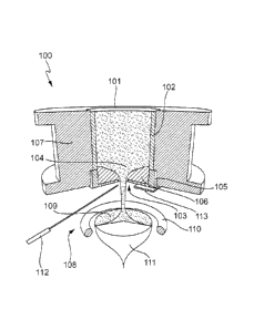
[0049] Figure 1 shows the schematic illustration of a
preferred embodiment of an installation 100 according
to the invention, which serves for producing a
monocrystalline semiconductor material.
[0050] As a source of a liquid semiconductor material
serving as starting material, the installation has the
reactor container 101. The reactor container,
illustrated in sectional view, comprises a cylindrical
section that is laterally delimited by the reactor
inner wall 102. The part of the reactor above the
cylindrical section is not illustrated; it comprises,
inter alia, an inlet for a silicon-containing plasma
and also an outlet for gases to be discharged from the
reactor. The plasma is generated from a carrier gas in
a device disposed upstream of the reactor container 101
and is admixed with particles of the semiconductor
material and/or a precursor compound of the
semiconductor material. Below the cylindrical section,
the interior of the reactor tapers towards the outlet
103, via which liquid semiconductor material 104 can
exit from the reactor container 101. The configuration
of this part of the interior of the reactor is given,
in particular, by the L-shaped cooled wall/bottom
CA 2795395 2017-07-24
ak 02795395 2012-10-02
- 18 -
elements 105 that are adjacent to the
underside of the reactor inner wall 102. These are kept
at a temperature below the melting point of the
semiconductor material contained in the reactor
container 101. Said material correspondingly forms a
solidified covering layer 106, which, if appropriate,
can also extend over the outlet 103 and thus block the
outlet. The reactor container 101 thus has a bottom
region which at least partly consists of the
semiconductor material to be produced. The reactor
outer wall 107 is arranged around the reactor inner
wall 102 and L-shaped cooled wall/bottom elements 105.
Said reactor outer wall can comprise heating,
insulating and/or cooling media.
[0051] The heating zone 108 is arranged below the
reactor container 101, a melt 109 composed of the
semiconductor material being situated in said heating
zone. The heating zone 108 comprises, as heating
medium, the induction heating system 110, which is
arranged around the melt 109 in a ring-shaped manner.
For said melt, the seed crystal 111 serves as a
substrate. It can be lowered together with the melt 109
from the heating zone 108 by means of suitable media,
such that, at the lower end of the melt 109, a
solidification front forms along which the
semiconductor material crystallizes in the
monocrystalline structure of the end cone 111.
[0052] The induction heating system 110 serves, in
particular, for maintaining the melt 109 in the heating
zone 108. Furthermore, however, it also heats the
bottom region of the reactor container 101. By turning
on the laser 112, which is arranged as a medium for the
controlled feeding of the liquid semiconductor material
serving as starting material into the melt 109 in such
a way that it can be focused onto the outlet 103, it is
possible to melt semiconductor material blocking the
outlet 103, if appropriate, such that the melt 109 can
ak 02795395 2012-10-02
=
- 19 -
be fed with liquid semiconductor material
in a controlled manner.
[0053] In order to prevent an uncontrolled discharge
from the reactor container 101, the installation 100
according to the invention comprises as a safeguard the
blocking means 113, which is a slide, by means of which
the outlet 103 can be closed off. The slide preferably
consists of a material which cannot be heated or can
scarcely be heated by high-frequency induction.