Note: Descriptions are shown in the official language in which they were submitted.
CA 02795737 2012-11-14
1
REGENERATIVE VARIABLE FREQUENCY DRIVE
[0001] This application claims the benefit under 35
U.S.C. 119(e) of the U.S. provisional patent application
no. 61/561,313 filed November 18, 2011.
Technical Field
[0002] The present invention relates to variable
frequency drives and more particularly to a regenerative
variable frequency drive with an active converter that
converts single-phase AC input to three-phase variable
frequency AC output.
Background Art
[0003] A variable frequency drive controls the speed and
torque of an alternating current (AC) motor by varying the
input frequency and voltage. Three-phase motors provide
higher mechanical efficiency, higher power factor and less
torque ripple than single-phase motors and are therefore a
more desirable choice. Variable frequency drives in the
past have generally included a diode rectifier, that
converts AC power to direct current (DC) power, connected
through a DC bus to an inverter that supplies three phase,
variable frequency AC power to a three-phase motor.
[0004] When a motor turns faster than the speed
designated by the variable frequency drive, the motor acts
as a generator, generating power that is returned to the DC
bus. In a variable frequency drive with a diode rectifier,
the rectification of the AC power to the DC bus is a one-
CA 02795737 2012-11-14
2
way street and the generated power causes the voltage on
the DC bus to rise.
[0005] One known method of handling the generated power
is to add a dynamic braking resistor to the variable
frequency drive. When the voltage on the DC bus rises due
to the generated power, the generated power is shunted to
the dynamic braking resistor that converts the generated
power to heat. Dynamic braking resistors add complexity and
expense to a variable frequency drive installation.
[0006] The generated power can alternatively be handled
with a regenerative variable frequency drive that has an
active converter instead of the one-way diode rectifier. An
active converter allows power to flow from the AC source to
the DC bus and from the DC bus back to the AC source. A
regenerative variable frequency drive puts the generated
power back onto the line, and thereby reduces the total
power consumption of the load.
[0007] Regenerative variable frequency drives with
three-phase active converters are known. A conventional
diode rectifier drive can convert AC power from a single-
phase source to charge the DC bus. The known three-phase
active converters cannot convert the power from a single-
phase AC source to charge the DC bus.
[0008] Three-phase AC power is generally supplied to
industrial areas. However, only single phase AC power is
available to most residential and rural areas. The single
phase AC power available in most residential and rural
CA 02795737 2012-11-14
3
areas is provided by a step down transformer connected to a
high voltage line and, in the United States, is normally
supplied as about 240 volts at 60 Hz between the first and
second input lines. Many three-phase induction motors are
operated at high voltage such as about 460 volts to reduce
the current passing between the inverter of the variable
frequency drive and the motor, and thereby reducing the
required size of the connecting cables. Diode rectifier
converters cannot directly boost the incoming 240 volts to
460 volts.
[0009] Diode rectifiers distort the current drawn from
the power grid. This distortion creates harmonic
distortions that may affect other users on the grid. The
distortion also reduces the power factor. A variable
frequency drive with a diode rectifier therefore requires
additional circuitry for power factor correction and
harmonic filtering.
Disclosure of the Invention
[00010] A regenerative variable frequency drive for
converting single phase AC power to variable frequency
three phase AC power includes an active converter that
converts single phase AC power to DC power and DC power to
single phase AC power and an inverter that converts DC
power to variable frequency, three phase AC power, and
variable frequency, three phase AC power to DC power. The
converter includes first and second input lines that
connect to a single phase AC power source, first and second
inductors, a filter capacitor, active half bridge first and
CA 02795737 2012-11-14
4
second modules, a positive bus bar, a negative bus bar,
first and second bus capacitors and a controller. The
inductors each have two coils and are connected in series
with the filter capacitor connecting between the coils,
between the inductors. The input lines connect to the
coils, with one coil connecting to the first module and the
other coil connecting to the second module, opposite the
terminals. The modules each have a pair of switches and a
pair of diodes, and each connect to the positive and
negative bus bars. The bus capacitors connect together in
series and connect between the positive and negative bus
bars. The bus bars connect to the inverter. The controller
monitors voltages and input current, and drives the
switches with a pulse width modulated signal having a
modulation index. The controller adjusts the modulation
index to maintain a selected voltage between the bus bars,
to provide correctly phased sinusoidal current from and to
the power grid and to boost the single phase AC input
voltage.
Brief Description of the Drawings
[00011] Details of this invention are described in
connection with the accompanying drawings that bear similar
reference numerals in which:
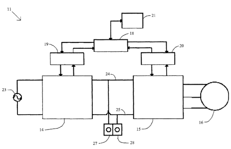
[00012] Figure 1 is a block diagram of a variable
frequency drive embodying the features of the present
invention.
CA 02795737 2012-11-14
5
[00013] Figure 2 is a schematic diagram of the active
converter of Figure 1 with an LC filter.
[00014] Figure 3 is a schematic diagram of the active
converter of Figure 1 with an LCL filter.
Detailed Description Of The Invention
[00015] Referring to Figure 1, a regenerative variable
frequency drive 11, embodying the features of the present
invention, includes an active converter 14 connected to an
inverter 15. The inverter 15 connects to and drives a load
16, such as a motor. A master controller 18 controls the
drive 11. The master controller connects to an input
controller 19, an output controller 20 and a human
interface device 21.
[00016] The input controller 19 connects to and controls
the converter 14. The converter 14 connects to a single
phase AC power source 23. Generally, the source 23 will be
a utility power grid. In the United States, the source 23
will typically provide power at 240V at 60 Hz.
[00017] The converter 14 converts single phase AC power
to DC power and DC power to single phase AC power. The
converter 14 connects to and provides DC power to the
inverter 15 through a positive bus bar 24 and a negative
bus bar 25. The drive 11 includes a positive terminal 27
that connects to the positive bus bar 24 and a negative
terminal 28 that connects to the negative bus bar 25, so
that the drive 11 can provide DC power to a DC load.
CA 02795737 2012-11-14
6
[00018] The output controller 20 connects to and controls
the inverter 15. The inverter 15 draws DC power from the
positive and negative bus bars 24 and 25, and provides
variable frequency, three phase AC power to the load 16.
When the load 16 supplies power back to the inverter 15, as
with a motor overrunning, the inverter 15 converts the AC
power generated by the load 16 to DC power, and supplies
that DC power to the positive and negative bus bars 24 and
25. The human interface device 21 allows a user to set the
speed and direction of the load 16.
[00019] As shown in Figures 2 and 3, the converter 14
includes first and second input lines 31 and 32, a
precharging circuit 33, a filter 35, first and second
modules 36 and 37, first and second bus capacitors 39 and
40, first and second resistors 42 and 43, the positive and
negative bus bars 24 and 25, and the input controller 19.
The first and second input lines 31 and 32 connect to the
source 23. The precharging circuit 33 connects along the
second input line 32 and includes a fuse 46, two diodes 47
and a resistor 48 in connected in series circuit, and a
switch 49 connected in parallel to the series circuit.
[00020] The filter 35 in Figure 2 is an LC filter with a
first inductor 51 and a filter capacitor 52. The first
inductor 51 has a first coil 53 that connects to the first
input line 31 opposite the source 23 and a second coil 54
that connects to the precharging circuit 33 opposite the
source 23. The filter capacitor 52 connects from the first
coil 53 to the second coil 54, between the first inductor
51 and the source 23. The filter 35 in Figure 3 is an LCL
CA 02795737 2012-11-14
7
filter that additionally includes a second inductor 56
between the source 23 and the filter capacitor 52. The
second inductor 56 has a first coil 57 that connects to the
first input line 31 at one end and to the first coil 53 of
the first inductor 51 at the other end, and a second coil
58 that connects from the precharging circuit 33 to the
second coil 54 of the first inductor 51.
[00021] The first and second modules 36 and 37 are each
active half bridges. The first module 36 has an input 61, a
positive output 62, a negative output 63, first and second
switches 65 and 66, and first and second diodes 67 and 68.
The input 61 connects to the first coil 53 of the first
inductor 51 opposite the source 23. The first and second
switches 65 and 66 are preferably solid state switches and
more preferably Insulated Gate Bipolar Transistors (IGBT).
Other switches such as bipolar junction transistors or
devices developed in the future might also be used.
[00022] The first switch 65 has a collector 70, a base
71 and an emitter 72. The second switch 66 has a collector
74, a base 75 and an emitter 76. The first diode 67 has an
anode 78 and a cathode 79, and the second diode 68 has an
anode 81 and a cathode 82. The input 61 connects to the
emitter 72 of the first switch 65, the collector 74 of the
second switch 66, the anode 78 of the first diode 67 and
the cathode 82 of the second diode 68. The collector 70 of
the first switch 65 and the cathode 79 of the first diode
67 connect to the positive output 62. The emitter 76 of the
second switch 66 and the anode 81 of the second diode 68
connect to the negative output 63. The positive output 62
CA 02795737 2012-11-14
8
connects to the positive bus bar 24 and the negative output
63 connects to the negative bus bar 25.
[00023] The second module 37 has an input 85, a positive
output 86, a negative output 87, first and second switches
89 and 90, and first and second diodes 91 and 92. The input
85 connects to the second coil 54 of the first inductor 51
opposite the source 23. The first and second switches 91
and 92 are preferably solid state switches and more
preferably Insulated Gate Bipolar Transistors (IGBT). Other
switches such as bipolar junction transistors or devices
developed in the future might also be used.
[00024] The first switch 89 has a collector 94, a base
95 and an emitter 96. The second switch 90 has a collector
98, a base 99 and an emitter 100. The first diode 91 has an
anode 102 and a cathode 103, and the second diode 92 has an
anode 105 and a cathode 106. The input 85 connects to the
emitter 96 of the first switch 89, the collector 98 of the
second switch 90, the anode 102 of the first diode 91 and
the cathode 106 of the second diode 92. The collector 94 of
the first switch 89 and the cathode 103 of the first diode
91 connect to the positive output 86. The emitter 100 of
the second switch 90 and the anode 105 of the second diode
92 connect to the negative output 87. The positive output
86 connects to the positive bus bar 24 and the negative
output 87 connects to the negative bus bar 25.
[00025] The first and second bus capacitors 39 and 40 are
connected together in series at connection node 108. The
first bus capacitor 39 connects to the positive bus bar 24
CA 02795737 2012-11-14
9
opposite connection node 108, and the second bus capacitor
40 connects to the negative bus bar 25 opposite the
connection node 108. One end of first resistor 42 connects
to the positive bus bar 24 and the other end of first
resistor 42 connects to the connection node 108. One end of
second resistor 43 connects to the negative bus bar 25 and
the other end of second resistor 43 connects to the
connection node 108. The first and second resistors 42 and
43 are balancing resistors that insure that the voltage
between the positive bus bar 24 and the connection node 108
equals the voltage between the connection node 108 and the
negative bus bar 25.
[00026] The input controller 19 connects to the bases 71,
75, 95 and 99 of the first switches 65 and 89 and the
second switches 66 and 90 of the first and second modules
36 and 37, and drives the first switches 65 and 89 and the
second switches 66 and 90 of the first and second modules
36 and 37. The input controller 19 connects to the first
and second input lines 31 and 32, to opposite ends of the
filter capacitor 52, and to the positive and negative bus
bars 24 and 25 to monitor input current and voltage,
voltage across the filter capacitor 52, and the voltage
between the positive and negative bus bars 24 and 25.
[00027] To avoid excessively high input current when
power is applied to the converter 14, switch 49 is
initially open and pre-charging current is supplied through
the diodes 47 and the current-limiting resistor 48 in the
precharging circuit 33. After the first and second bus
CA 02795737 2012-11-14
10
capacitors 39 and 40 are charged, the switch 49 is closed
to bypass resistor 48.
[00028] The input voltage is V12=V1-V2, the voltage across
the filter capacitor 52 is vab=Va-Vb, the voltage at the
connection node 108 is V, and the voltage between the
positive and negative bus bars 24 and 25 is 2Vd0=(Vpus-
Vz)+ (Vz-VNEG)= The first module 36 is driven to produce a
pulse width modulated signal at input 61 that has an
average value given by:
[00029] vaz=VdcMcos((oot),
[00030] The second module 37 is driven to produce a pulse
width modulated signal at input 85 that has an average
value given by:
[00031] Vbz = ¨VdcMCOS(C000 =
[00032] where M is the modulation index (0 <= M <= 1), co,
is the frequency of the input voltage, and cos(o)t) is the
cosine of the input voltage frequency (1 => cos(wot) => -1).
The difference in voltage between the input 61 of the first
module 36 and the input 85 of the second module 37 is given
by:
[00033] Vab = Vaz Vbz = 2 VdcMCOS(Wot).
[00034] As long as the value 2Vd, is greater than the peak
value of the input voltage V12, at any instant in time the
value of M can be adjusted to make vab at that instant
either less than, equal to, or greater than the input
voltage V12. The input voltage V12 is separated from the
CA 02795737 2012-11-14
11
voltage vat, by the first inductor 51 in Figure 2, and the
first and second inductors 51 and 56 in Figure 3, so that:
(1) if V12 and v,b are equal there will be no change in the
current through the inductors, (2) if V12 is greater than Vat)
the current through the inductors will increase, or (3) if
V12 is less than vab the current through the inductors will
decrease. The input controller 19 can make instantaneous
adjustments to the value of M to induce any desired value
of input current. The input current can be controlled so
that the average value of the voltage 2Vdc, remains constant
even though electrical charge is being removed from the
first and second bus capacitors 39 and 40 by the inverter
15. The value of M can also be adjusted so that the input
current is sinusoidal. If the converter 14 is delivering
power to the inverter 15 and subsequently to the load 16,
then the input current will need to be in phase with the
input voltage. If the load 16 is delivering power to the
converter then the input current will need to be 180
degrees out of phase with the input voltage.
[00035] The converter 14 can also boost the voltage of
the incoming power. As an example, and not as a limitation,
the converter can boost single phase 240 volt AC power to
460 volts. When V12 > 0, the second switch 66 of the first
module 36 is turned on, and current flows from the source
23 through the first coil 53 of the first inductor 51,
through the input 61 and second switch 66 of the first
module 36, through the negative bus bar 25, through the
second diode 92 and input 85 of the second module 37,
through the second coil 54 of the first inductor 51 and
CA 02795737 2012-11-14
=
12
back to the source 23. The current will be a steadily
increasing ramp which will stop increasing only when the
second switch 66 of the first module 36 is turned off. Thus
the maximum current is determined by the width of the
controller pulse to the second switch 66 of the first
module 36. The ramp rate is determined by the inductance
values, the value of V12, and the equation V12 = L dI/dt.
[00036] When the second switch 66 of the first module 36
turns off, the first inductor 51 will develop a voltage
which keeps the current constant during the transition.
Current now flows from the source 23 through the first coil
53 of the first inductor 51, through the input 61 and first
diode 67 of the first module 36, through the positive bus
bar 24, through the first and second bus capacitors 39 and
40, through the second diode 92 and input 85 of the second
module 37, through the second coil 54 of the first inductor
51 and back to the source 23. This current charges the
first and second bus capacitors 39 and 40. During the
charging cycle the current decays at a rate determined by
the inductance value of the first inductor 51, the voltage
(V12-Vpos+VNEG) and the equation (V12- Vpos+VNEG) = LdI/dt. The
amount of charging current can have any desired value,
determined only by the width of the pulses, and the first
and second bus capacitors 39 and 40 can be charged to any
desired value. The charging sequence could also have been
implemented by switching the first switch 89 of the second
module 37. When the voltage V12 < 0, charging can be
implemented by switching either the first switch 65 of the
CA 02795737 2012-11-14
13
first module 36 or the second switch 90 of the second
module 37.
[00037] Although the present invention has been described
with a certain degree of particularity, it is understood
that the present disclosure has been made by way of example
and that changes in details of structure may be made
without departing from the spirit thereof.