Note: Descriptions are shown in the official language in which they were submitted.
CA 02795742 2012-10-05
WO 2011/127186 PCT/US2011/031439
ENHANCED BULK HETEROJUNCTION DEVICES PREPARED
BY THERMAL AND SOLVENT VAPOR ANNEALING PROCESSES
Cross-Reference to Related Applications
[0001] This application claims priority to U.S. Provisional Application Nos.
61/322,039, filed on April 8, 2010, and 61/393,646, filed October 15, 2010,
which are
both incorporated herein by reference in their entirety.
Statement Regarding Federally Sponsored Research
[0002] The subject matter of this application was prepared with U.S.
Government support under Contract No. DE-FG36-08GO18022 awarded by U.S.
Department of Energy, National Renewable Energy Laboratory. The government
has certain rights in the subject matter of this application.
Joint Research Agreement
[0003] The subject matter of this application was made by, on behalf of,
and/or in connection with one or more of the following parties to a joint
university-
corporation research agreement: University of Michigan and Global Photonic
Energy
Corporation. The agreement was in effect on and before the date the claimed
invention was made, and the claimed invention was made as a result of
activities
undertaken within the scope of the agreement.
Field of the Disclosure
[0004] The present disclosure generally relates to methods of preparing bulk
heterojunction organic photovoltaic cells by thermal and solvent vapor
annealing
processes. More specifically, it is directed to increasing the mesoscopic
order and
crystallinity of organic thin films by exposing bulk heterojunctions to
vaporized
solvents, as well as combinations of thermal and solvent vapor annealing.
CA 02795742 2012-10-05
WO 2011/127186 PCT/US2011/031439
Background
[0005] Optoelectronic devices rely on the optical and electronic properties of
materials to either produce or detect electromagnetic radiation electronically
or to
generate electricity from ambient electromagnetic radiation.
[0006] Photosensitive optoelectronic devices convert electromagnetic
radiation into electricity. Solar cells, also called photovoltaic (PV)
devices, are a type
of photosensitive optoelectronic device that is specifically used to generate
electrical
power. PV devices, which may generate electrical energy from light sources
other
than sunlight, can be used to drive power consuming loads to provide, for
example,
lighting, heating, or to power electronic circuitry or devices such as
calculators,
radios, computers or remote monitoring or communications equipment. These
power generation applications also often involve the charging of batteries or
other
energy storage devices so that operation may continue when direct illumination
from
the sun or other light sources is not available, or to balance the power
output of the
PV device with a specific application's requirements. As used herein the term
"resistive load" refers to any power consuming or storing circuit, device,
equipment
or system.
[0007] Another type of photosensitive optoelectronic device is a
photoconductor cell. In this function, signal detection circuitry monitors the
resistance of the device to detect changes due to the absorption of light.
[0008] Another type of photosensitive optoelectronic device is a
photodetector. In operation, a photodetector is used in conjunction with a
current
detecting circuit which measures the current generated when the photodetector
is
exposed to electromagnetic radiation and may have an applied bias voltage. A
detecting circuit as described herein is capable of providing a bias voltage
to a
-2-
CA 02795742 2012-10-05
WO 2011/127186 PCT/US2011/031439
photodetector and measuring the electronic response of the photodetector to
electromagnetic radiation.
[0009] These three classes of photosensitive optoelectronic devices may be
characterized according to whether a rectifying junction as defined below is
present,
and also according to whether the device is operated with an external applied
voltage, also known as a bias or bias voltage. A photoconductor cell does not
have
a rectifying junction and is normally operated with a bias. A PV device has at
least
one rectifying junction and is operated with no bias. A photodetector has at
least
one rectifying junction and is usually but not always operated with a bias. As
a
general rule, a photovoltaic cell provides power to a circuit, device or
equipment, but
does not provide a signal or current to control detection circuitry, or the
output of
information from the detection circuitry. In contrast, a photodetector or
photoconductor provides a signal or current to control detection circuitry, or
the
output of information from the detection circuitry but does not provide power
to the
circuitry, device or equipment.
[0010] Traditionally, photosensitive optoelectronic devices have been
constructed of a number of inorganic semiconductors, e.g., crystalline,
polycrystalline
and amorphous silicon, gallium arsenide, cadmium telluride and others. Herein,
the
term "semiconductor" denotes materials which can conduct electricity when
charge
carriers are induced by thermal or electromagnetic excitation. The term
"photoconductive" generally relates to the process in which electromagnetic
radiant
energy is absorbed and thereby converted to excitation energy of electric
charge
carriers so that the carriers can conduct, i.e., transport, electric charge in
a material.
The terms "photoconductor" and "photoconductive material" are used herein to
refer
-3-
CA 02795742 2012-10-05
WO 2011/127186 PCT/US2011/031439
to semiconductor materials which are chosen for their property of absorbing
electromagnetic radiation to generate electric charge carriers.
[0011] PV devices may be characterized by the efficiency with which they can
convert incident solar power to useful electric power. Devices utilizing
crystalline or
amorphous silicon dominate commercial applications, and some have achieved
efficiencies of 23% or greater. However, efficient crystalline-based devices,
especially of large surface area, are difficult and expensive to produce due
to the
problems inherent in producing large crystals without significant efficiency-
degrading
defects. On the other hand, high efficiency amorphous silicon devices still
suffer
from problems with stability. Present commercially available amorphous silicon
cells
have stabilized efficiencies between 4 and 8%.
[0012] PV devices may be optimized for maximum electrical power generation
under standard illumination conditions (i.e., Standard Test Conditions which
are
1000 W/m2, AM1.5 spectral illumination), for the maximum product of
photocurrent
times photovoltage. The power conversion efficiency of such a cell under
standard
illumination conditions depends on the following three parameters: (1) the
current
under zero bias, i.e., the short-circuit current /sc, in Amperes, (2) the
photovoltage
under open circuit conditions, i.e., the open circuit voltage Voc, in Volts,
and (3) the
fill factor, if
[0013] PV devices produce a photo-generated current when they are
connected across a load and are irradiated by light. When irradiated under
infinite
load, a PV device generates its maximum possible voltage, V open-circuit, or
Voc.
When irradiated with its electrical contacts shorted, a PV device generates
its
maximum possible current, I short-circuit, or Isc. When actually used to
generate
power, a PV device is connected to a finite resistive load and the power
output is
-4-
CA 02795742 2012-10-05
WO 2011/127186 PCT/US2011/031439
given by the product of the current and voltage, I XV. The maximum total power
generated by a PV device is inherently incapable of exceeding the product, Isc
x
Voc. When the load value is optimized for maximum power extraction, the
current
and voltage have the values, Imax and Vmax, respectively.
[0014] A figure of merit for PV devices is the fill factor, if, defined as:
if = { Imax Vmax }/{ Isc Voc } (1)
where if is always less than 1, as Isc and Voc are never obtained
simultaneously in
actual use. Nonetheless, as if approaches 1, the device has less series or
internal
resistance and thus delivers a greater percentage of the product of Isc and
Voc to the
load under optimal conditions. Where Pinc is the power incident on a device,
the
power efficiency of the device, rip, may be calculated by:
11P = ff * (Isc * Voc) / Pinc
[0015] To produce internally generated electric fields that occupy a
substantial
volume of the semiconductor, the usual method is to juxtapose two layers of
material
with appropriately selected conductive properties, especially with respect to
their
distribution of molecular quantum energy states. The interface of these two
materials is called a photovoltaic junction. In traditional semiconductor
theory,
materials for forming PV junctions have been denoted as generally being of
either n
or p type. Here n-type denotes that the majority carrier type is the electron.
This
could be viewed as the material having many electrons in relatively free
energy
states. The p-type denotes that the majority carrier type is the hole. Such
material
has many holes in relatively free energy states. The type of the background,
i.e., not
photo-generated, majority carrier concentration depends primarily on
unintentional
doping by defects or impurities. The type and concentration of impurities
determine
the value of the Fermi energy, or level, within the gap between the conduction
band
-5-
CA 02795742 2012-10-05
WO 2011/127186 PCT/US2011/031439
minimum and valance band maximum energies. The Fermi energy characterizes the
statistical occupation of molecular quantum energy states denoted by the value
of
energy for which the probability of occupation is equal to '/. A Fermi energy
near
the conduction band minimum energy indicates that electrons are the
predominant
carrier. A Fermi energy near the valence band maximum energy indicates that
holes
are the predominant carrier. Accordingly, the Fermi energy is a primary
characterizing property of traditional semiconductors and the prototypical PV
junction
has traditionally been the p-n interface.
[0016] The term "rectifying" denotes, inter alia, that an interface has an
asymmetric conduction characteristic, i.e., the interface supports electronic
charge
transport preferably in one direction. Rectification is associated normally
with a built-
in electric field which occurs at the junction between appropriately selected
materials.
[0017] Conventional inorganic semiconductor PV cells employ a p-n junction
to establish an internal field. Early organic thin film cells, such as
reported by Tang,
App!. Phys Lett. 48, 183 (1986), contain a heterojunction analogous to that
employed
in a conventional inorganic PV cell. However, it is now recognized that in
addition to
the establishment of a p-n type junction, the energy level offset of the
heterojunction
also plays an important role.
[0018] The energy level offset at the organic D-A heterojunction is believed
to
be important to the operation of organic PV devices due to the fundamental
nature of
the photo-generation process in organic materials. Upon optical excitation of
an
organic material, localized Frenkel or charge-transfer excitons are generated.
For
electrical detection or current generation to occur, the bound excitons must
be
dissociated into their constituent electrons and holes. Such a process can be
-6-
CA 02795742 2012-10-05
WO 2011/127186 PCT/US2011/031439
induced by the built-in electric field, but the efficiency at the electric
fields typically
found in organic devices (F - 106 V/cm) is low. The most efficient exciton
dissociation in organic materials occurs at a donor-acceptor (D-A) interface.
At such
an interface, the donor material with a low ionization potential forms a
heterojunction
with an acceptor material with a high electron affinity. Depending on the
alignment
of the energy levels of the donor and acceptor materials, the dissociation of
the
exciton can become energetically favorable at such an interface, leading to a
free
electron polaron in the acceptor material and a free hole polaron in the donor
material.
[0019] Organic PV cells have many potential advantages when compared to
traditional silicon-based devices. Organic PV cells are light weight,
economical in
materials use, and can be deposited on low cost substrates, such as flexible
plastic
foils. However, organic PV devices typically have relatively low external
quantum
efficiency (electromagnetic radiation to electricity conversion efficiency),
being on the
order of 1 % or less. This is, in part, thought to be due to the second order
nature of
the intrinsic photoconductive process. That is, carrier generation requires
exciton
generation, diffusion and ionization or collection. There is an efficiency rl
associated
with each of these processes. Subscripts may be used as follows: P for power
efficiency, EXT for external quantum efficiency, A for photon absorption, ED
for
diffusion, CC for collection, and INT for internal quantum efficiency. Using
this
notation:
11P"'11EXT71A*TIED *1ICC
71EXT = '-IA * l INT
[0020] The diffusion length (LD) of an exciton is typically much less (LD -
50A)
than the optical absorption length (-500A), requiring a trade-off between
using a
-7-
CA 02795742 2012-10-05
WO 2011/127186 PCT/US2011/031439
thick, and therefore resistive, cell with multiple or highly folded
interfaces, or a thin
cell with a low optical absorption efficiency.
[0021] Several methods for making bulk heterojunction (BHJ) devices include
phase separation during spin-coating of polymers, phase segregation from a
donor-
acceptor mixture induced by high temperature annealing of small-molecular-
weight
organic layers, and controlled growth of small-molecular-weight organic layers
with
Organic Vapor Phase Deposition.
[0022] One challenge for efficient bulk heterojunction solar cells is to
generate
a maximized interface between donor and acceptor materials within the
photoactive
layer to ensure efficient dissociation of the excitons, while typical
dimensions of
phase separation are within the exciton diffusion range and continuous
pathways for
transport of charge carriers to the electrode. To realize an ideal material
system and
blend structure for efficient solar cells, it may be desirable to manipulate
the donor-
acceptor blend morphology and crystallinity through one or more annealing
processes, such as thermal and solvent vapor annealing.
[0023] While the spin-cast process provides a simple and convenient way to
prepare homogeneous thin films, the solvent may evaporate quickly during its
process and phase separation of intimately mixed donor and acceptor materials
may
be suppressed. Because organic materials may form amorphous, crystalline, or
semi-crystalline structures during casting from solution, different
evaporation times
for different solvents may affect the dynamic assembly process of the organic
molecules. This, in turn, may determine the microstructure and morphology of
active
layer, and the resulting variability in carrier transport properties and
device
performance. Thus, thin films obtained from spin coating are typically not in
their
thermodynamically equilibrium state, such that thermodynamic forces drive the
films
-8-
CA 02795742 2012-10-05
WO 2011/127186 PCT/US2011/031439
to reorganize toward the stable equilibrium state. This evolution may be
accelerated
at elevated temperature or solvent vapor pressure.
[0024] In organic semiconductive materials, post-annealing may enhance the
charge carrier transport by increasing the mesoscopic order and crystallinity,
which
can manifest itself in maximizing intermolecular 7T-7T stacking. In general,
the
performance of bulk solar cells can be optimized by controlling the nanometer
morphology of the active layer. For small molecule bulk solar cells, thermal
annealing processes have been explored in DPP(TBFu)2/PC70BM systems to
increase charge-carrier mobility and improve carrier collection.
[0025] Alternatively, solvent vapor annealing may be useful for active-layer
morphology control and optimizations. Here, the atmosphere saturates with
solvent
rapidly and allows the film-formation kinetics to be prolonged further. This
further
film formation, like thermal annealing, may lead to improved interpenetration
of the
donor/acceptor domains as well as the increased order within donor domains.
Accordingly, there remains a need to further develop active-layer morphology
control
and optimizations. Applicants describe herein solvent vapor annealing
processes
that not only meets this need, but which can be used to prepare bulk
heterojunction
devices with enhanced performance characteristics. Applicants also described
combinations of thermal and solvent vapor annealing that result in optimized
active-
layer morphologies and bulk heterojunction devices with enhanced performance
characteristics.
Summary
[0026] There are disclosed methods of preparing bulk heterojunction organic
photosensitive devices comprising exposure to certain thermal and/or solvent
vapor
-9-
CA 02795742 2012-10-05
WO 2011/127186 PCT/US2011/031439
annealing processes. In one embodiment, a method of preparing a photosensitive
device comprises:
providing a structure comprising at least one electrode and a bulk
heterojunction, wherein the bulk heterojunction comprises at least one first
photoactive material and at least one second photoactive material;
providing at least one solvent;
vaporizing at least a portion of the solvent; and
exposing at least a portion of the structure to the vaporized solvent, wherein
the exposure to the vaporized solvent increases the crystallinity of at least
one of the
first and second photoactive materials.
[0027] In some embodiments, the method further comprises thermally
annealing the structure. In some embodiments, the thermal annealing step takes
place after exposing at least a portion of the structure to the vaporized
solvent.
[0028] In another embodiment, there is described a method of enhancing the
crystallinity of a bulk heterojunction in a photosensitive device, the bulk
heterojunction comprising at least one first and at least one second organic
photoactive material. In one embodiment, the method comprises:
exposing at least a portion of the bulk heterojunction to a vaporized solvent,
wherein the photosensitive device exhibits one or more of the following
characteristics when compared to the device without exposure to the vaporized
solvent:
increased fill factor (FF);
increased external quantum efficiency (EQE); and
increased current density versus voltage (J-V).
-10-
CA 02795742 2012-10-05
WO 2011/127186 PCT/US2011/031439
[0029] In some embodiments, the method further comprises thermally
annealing the structure. In some embodiments, the thermal annealing step takes
place after exposing at least a portion of the structure to the vaporized
solvent.
Brief Description of the Drawings
[0030] The accompanying drawings, which are incorporated in and constitute
a part of this specification, illustrate several embodiments described herein
and,
together with the description, serve to explain the principles of this
application. The
figures are not necessarily drawn to scale.
[0031] FIG. 1A illustrates the XRD (x-ray diffraction data) for SQ:PC70BM
(1:6)
bulk solar cells cast from chloroform and thermally annealed at various
temperatures
for a period of 10 minutes, and SQ: PC7oBM (1:6) bulk solar cells cast from
chloroform and solvent annealed with dicloromethane for various exposure
periods.
[0032] FIG. 1B-1D illustrates the RMS (root-mean-square) roughness for
SQ:PC70BM (1:6) bulk solar cells as-cast from chloroform, thermally annealed
at
70 C for 10 minutes, and solvent annealed with dichloromethane for 12 minutes,
respectively.
[0033] FIG. 2A illustrates FF versus power intensity for SQ:PC70BM (1:6) bulk
solar cells cast from chloroform and thermally annealed at various
temperatures.
[0034] FIG. 2B illustrates FF versus power intensity for SQ:PC70BM (1:6) bulk
solar cells cast from chloroform and solvent annealed with dichloromethane for
various exposure periods.
[0035] FIG. 2C illustrates FF versus power intensity for SQ:PC70BM (1:6) bulk
solar cells cast from 1,2-dichlorobenzene and solvent annealed with
dichloromethane for various exposure periods.
-11-
CA 02795742 2012-10-05
WO 2011/127186 PCT/US2011/031439
[0036] FIG. 3A illustrates EQE for SQ:PC70BM (1:6) bulk solar cells cast from
1,2-dichlorobenzene and solvent annealed with dichloromethane for various
exposure periods.
[0037] FIG. 3B illustrates J-V for bulk heterojunction devices cast from 1,2-
dichlorobenzene and solvent annealed with dichloromethane for various exposure
periods.
[0038] FIG. 3C illustrates rip versus power intensity for bulk heterojunction
devices cast from 1,2-dichlorobenzene and solvent annealed with
dichloromethane
for various exposure periods.
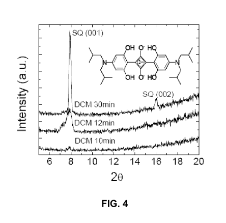
[0039] FIG. 4 illustrates the XRD for SQ:PC7oBM (1:6) bulk solar cells cast
from DCB and solvent annealed with dicloromethane for various exposure
periods.
[0040] FIG. 5A-5C illustrates the RMS of bulk heterojunction devices as-cast
from DCB, solvent annealed with dichloromethane for 12 minutes, and solvent
annealed with dichloromethane for 30 minutes, respectively.
[0041] FIG. 6A illustrates the absorption coefficients for SQ:PC70BM (1:6)
bulk
solar cells cast from DCB and solvent annealed with dichloromethane for
various
exposure periods.
[0042] FIG. 6B illustrates the PL (photoluminescence) intensity for
SQ:PC70BM (1:6) bulk solar cells cast from DCB and solvent annealed with
dichloromethane for various exposure periods (see FIG. 6A legend).
[0043] FIG. 6C illustrates the EQE for SQ:PC70BM (1:6) bulk solar cells cast
from DCB and solvent annealed with dichloromethane for various exposure
periods
(see FIG. 6A legend).
-12-
CA 02795742 2012-10-05
WO 2011/127186 PCT/US2011/031439
[0044] FIG. 6D illustrates the current density versus V (voltage) for
SQ:PC70BM (1:6) bulk solar cells cast from DCB and solvent annealed with
dichloromethane for various exposure periods (see FIG. 6A legend).
[0045] FIG. 7A illustrates ilp versus power intensity for SQ:PC70BM (1:6) bulk
solar cells cast from DCB and solvent annealed with dichloromethane for
various
exposure periods.
[0046] FIG. 7B illustrates FF versus power intensity for SQ:PC70BM (1:6) bulk
solar cells cast from DCB and solvent annealed with dichloromethane for
various
exposure periods.
[0047] FIG. 8A illustrates the XRD (x-ray diffraction) data for several SQ:C60
planar cells thermally annealed at various temperatures for a period of 20
minutes.
[0048] FIG. 8B illustrates EQE for the planar SQ:C60 devices tested in FIG.
8A.
[0049] FIG. 9A illustrates illustrates rip versus power intensity for the
planar
SQ:C60 devices tested in FIG. 8A.
[0050] FIG. 9B illustrates FF versus power intensity for the planar SQ:C60
devices tested in FIG. 8A.
[0051] FIG. 10A illustrates the XPS (x-ray photoelectron spectroscopy)
measurements for several SQ:PC70BM (1:6) bulk heterojunction devices cast from
DCB and thermally annealed at various temperatures for a period of 10 minutes.
[0052] FIG. 10B illustrates AFM (atomic force microscopy) measurements the
SQ:PC70BM (1:6) bulk heterojunction devices described in FIG. 10A.
[0053] FIG. 11A illustrates rlp versus power intensity for the SQ:PC70BM (1:6)
bulk heterojunction devices tested in FIG. 10A.
-13-
CA 02795742 2012-10-05
WO 2011/127186 PCT/US2011/031439
[0054] FIG. 11B illustrates FF versus power intensity for the SQ:PC7oBM (1:6)
bulk heterojunction devices tested in FIG. 10A.
[0055] FIG. 12A illustrates the RMS (roughness measurement system) of an
SQ:PC70BM (1:6) bulk heterojunction device as-cast from DCB.
[0056] FIG. 12B illustrates the RMS roughness of an SQ:PC70BM (1:6) bulk
heterojunction device cast from DCB, followed by thermal annealing at 70 C.
[0057] FIG. 12C illustrates the RMS roughness of an SQ:PC70BM (1:6) bulk
heterojunction cast from DCB, followed by solvent vapor annealing with
dichloromethane for 30 minutes and thermal annealing at 50 C.
[0058] FIG. 12D illustrates the RMS roughness of an SQ:PC70BM (1:6) bulk
heterojunction device cast from DCB, followed by thermal annealing at 110 C.
[0059] FIG. 12E illustrates XRD data for SQ:PC70BM (1:6) bulk heterojunction
devices cast from DCB, followed by solvent vapor annealing with
dichloromethane
for various time periods, and thermally annealed at 50 C.
[0060] FIG. 13A illustrates rip versus power intensity for the SQ:PC70BM (1:6)
bulk heterojunction devices cast from DCB, followed by solvent vapor annealing
with
dichloromethane for various time periods and thermal annealing at 50 C.
[0061] FIG. 13B illustrates FF versus power intensity for the SQ:PC7oBM (1:6)
bulk heterojunction devices tested in FIG. 13A.
[0062] FIG. 14 illustrates EQE for the SQ:PC70BM (1:6) bulk heterojunction
devices tested in FIG. 13A.
[0063] FIG. 15 illustrates rlpsummary of SQ/C60 planar cells as-cast and
thermally annealed at various temperatures, SQ:PC7oBM (1:6) bulk cells as-cast
and
-14-
CA 02795742 2012-10-05
WO 2011/127186 PCT/US2011/031439
thermally annealed at various temperatures, and SQ:PC70BM (1:6) bulk cells as-
cast
and DCM solvent annealed for 2 min, 6 min, 8 min and 12 min at I sun
illumination.
Detailed Description of the Invention
Definitions
[0064] As used herein, the term "organic" includes polymeric materials as well
as small molecule organic materials that may be used to fabricate organic
optoelectronic devices. "Small molecule" refers to any organic material that
is not a
polymer, and "small molecules" may actually be quite large. Small molecules
may
include repeat units in some circumstances. For example, using a long chain
alkyl
group as a substituent does not remove a molecule from the "small molecule"
class.
Small molecules may also be incorporated into polymers, for example as a
pendent
group on a polymer backbone or as a part of the backbone. Small molecules may
also serve as the core moiety of a dendrimer, which consists of a series of
chemical
shells built on the core moiety. The core moiety of a dendrimer may be a
fluorescent
or phosphorescent small molecule emitter. A dendrimer may be a "small
molecule."
In general, a small molecule has a defined chemical formula with a molecular
weight
that is the same from molecule to molecule, whereas a polymer has a defined
chemical formula with a molecular weight that may vary from molecule to
molecule.
As used herein, "organic" includes, but is not limited to, metal complexes of
hydrocarbyl and heteroatom-substituted hydrocarbyl ligands.
[0065] Methods and processes are described herein for using solvent
annealing, and specifically solvent vapor annealing, and thermal annealing
during
the preparation bulk heterojunction organic photovoltaic cells. The morphology
and
phase separation of the organic materials may be important in that they enable
both
-15-
CA 02795742 2012-10-05
WO 2011/127186 PCT/US2011/031439
charge separation and collection. The solvent vapor annealing process
described
herein may be useful in having a templating effect on one or more of the
organic
photoactive materials comprising the bulk heterojunction, which results in the
self-
assembling of the organic material to form ordered aggregates. Nanomorphology
and crystallinity of the organic materials may be dependent on solvent type
and
duration. In some embodiments, the solvent vapor annealing and/or thermal
annealing processes described herein may be capable of increasing the
crystalline
features of one or more of the organic materials comprising a bulk
heterojunction
blend that is largely amorphous in nature as cast.
[0066] In one embodiment, there is described a method of preparing a
photosensitive device which comprises:
providing a structure comprising at least one electrode and a bulk
heterojunction, wherein the bulk heterojunction comprises at least one first
organic
photoactive material and at least one second organic photoactive material;
providing at least one solvent;
vaporizing at least a portion of the solvent; and
exposing at least a portion of the structure to the vaporized solvent, wherein
the exposure increases the crystallinity of at least one of the first or
second organic
photoactive materials.
[0067] In some embodiments, the method further comprises thermally
annealing the structure. In some embodiments, the thermal annealing step takes
place after exposing at least a portion of the structure to the vaporized
solvent.
[0068] In some embodiments, the structure may be prepared by depositing
the at least one first and the at least one second organic photoactive
materials over
-16-
CA 02795742 2012-10-05
WO 2011/127186 PCT/US2011/031439
the first electrode. After the annealing process is complete, a second
electrode may
be patterned over the bulk heterojunction.
[0069] Electrodes, such as anodes and cathodes, may be composed of
metals or "metal substitutes." Herein the term "metal" is used to embrace both
materials composed of an elementally pure metal, and also metal alloys which
are
materials composed of two or more elementally pure metals. The term "metal
substitute" refers to a material that is not a metal within the normal
definition, but
which has the metal-like properties such as conductivity. Metal substitutes
include,
for example, doped wide-bandgap semiconductors, degenerate semiconductors,
conducting oxides, and conductive polymers.
[0070] The term "cathode" is used in the following manner. In a non-stacked
PV device or a single unit of a stacked PV device under ambient irradiation
and
connected with a resistive load and with no externally applied voltage, e.g.,
a PV
device, electrons move to the cathode from the photo-conducting material.
Similarly,
the term "anode" is used herein such that in a PV device under illumination,
holes
move to the anode from the photoconducting material, which is equivalent to
electrons moving in the opposite manner. It will be noted that as the terms
are used
herein, anodes and cathodes may be electrodes or charge transfer layers.
[0071] Electrodes may comprise a single layer or multiple layers (a
"compound" electrode), and may be transparent, semi-transparent, or opaque.
Examples of electrodes and electrode materials include, but are not limited
to, those
disclosed in U.S. Patent No. 6,352,777 to Bulovic et al., and U.S. Patent No.
6,420,031, to Parthasarathy, et al., each incorporated herein by reference for
disclosure of these respective features. As used herein, a layer is said to be
-17-
CA 02795742 2012-10-05
WO 2011/127186 PCT/US2011/031439
"transparent" if it transmits at least 50% of the ambient electromagnetic
radiation in a
relevant wavelength.
[0072] In one embodiment, the first electrode may comprise an interfacial
layer comprising molybdenum oxide (MoOx). MoOx is an exemplary interfacial
layer
in organic PV cells, which is believed to serve to reduce dark current and
increase
open circuit voltage (Li, N. et al,. Open circuit voltage enhancement due to
reduced
dark current in small molecule photovoltaic cells, Appl. Phys. Left., 94,
023307, Jan.
2009).
[0073] In some embodiments, the first organic photoactive material may
comprise a donor-type material. Non-limiting examples of the first organic
photoactive material that may be used herein include subphthalocyanine
(SubPc),
copper pthalocyanine (CuPc), chloroaluminium phthalocyanine (CIAIPc), tin
phthalocyanine (SnPc), pentacene, tetracene, diindenoperylene (DIP), and
squaraine (SQ).
[0074] In some embodiments, the second organic photoactive material may
comprise an acceptor-type material. Non-limiting examples of second organic
photoactive materials that may be used herein include C60, C70, [6,6]-phenyl
C70
butyric acid methyl ester (PC70BM), 3,4,9,10-perylenetetracarboxylicbis-
benzimidazole (PTCBI), and hexadecafluorophthalocyanine (F16CuPc).
[0075] In another embodiment, a blocking layer may be included, such as
between the bulk heterojunction and the second electrode. Examples of exciton
blocking layers (EBLs) are described in U.S. Patent No. 6,451,415 and
7,230,269 to
Forrest et al., which are incorporated herein by reference for their
disclosures related
to EBLs. Additional background explanation of EBLs may also be found in
Peumans
et al., "Efficient photon harvesting at high optical intensities in ultrathin
organic
-18-
CA 02795742 2012-10-05
WO 2011/127186 PCT/US2011/031439
double-heterostructure photovoltaic diodes," Applied Physics Letters 76, 2650-
52
(2000), which is also incorporated herein by reference. EBLs are believed to
reduce
quenching by preventing excitons from migrating out of the donor and/or
acceptor
materials. Non-limiting examples of the exciton blocking layer that may be
used
herein include bathocuproine (BCP), bathophenanthroline (BPhen), 3,4,9,10-
perylenetetracarboxylicbis-benzimidazole (PTCBI), 1,3,5-tris(N-
phenylbenzimidazol-
2-yl)benzene (TPBi), tris(acetylacetonato) ruthenium(III) (RuAcaca3), and
aluminum(III)phenolate (Alq2 OPH).
[0076] Examples of the second electrode that may be used herein include a
metal substitute, a non-metallic material or a metallic material chosen from,
for
example, Ag, Au, and Al.
[0077] It is appreciated that the first electrode may comprise a conducting
oxide, such as one chosen from indium tin oxide (ITO), tin oxide (TO), gallium
indium
tin oxide (GITO), zinc oxide (ZO), and zinc indium tin oxide (ZITO), and the
transparent conductive polymers comprises polyanaline (PANT). In one
embodiment,
the bulk heterojunction organic photovoltaic cell comprises:
ITO/Mo03/SQ:PC70BM/LiF/AI; and
ITO/Mo03/SQ: PC70BM/C60/BCP/LiF/Al.
[0078] The organic layers described herein may have thicknesses ranging
from 25-1200 A, such as 50-950 A, or even 100-700 A.
[0079] In some embodiments, a bulk heterojunction may be made, for
example, by vacuum thermal evaporation (VTE), spin coating, or organic vapor
phase deposition (OVPD). OVPD is different from vacuum thermal evaporation
(VTE) in that OVPD uses a carrier gas to transport vapors into a deposition
chamber.
Spatially separating the functions of evaporation and transport leads to
precise
-19-
CA 02795742 2012-10-05
WO 2011/127186 PCT/US2011/031439
control over the deposition process, and enabling control over the organic
surface
morphology, e.g., flat with smooth surface or layers with protrusions.
[0080] In one embodiment, the bulk heterojunction is prepared by spin
coating. The use of different solvent systems when preparing bulk
heterojunctions
via spin coating may have an effect on the ultimate efficiency of the
photosensitive
device upon completion. For example, devices may be made with solvents having
a
lower boiling point temperature, or those with a higher boiling point. Because
low
boiling-point solvents evaporate quickly, it may be desirable to use higher
boiling-
point solvents to further control morphology. In some embodiments, the use of
solvents like 1,2-dichlorobenzene (DCB) in the initial preparation of the bulk
heterojunction may ultimately result in PV devices exhibiting improved
performance
properties after solvent vapor annealing when compared to those prepared with
lower boiling-point solvents.
[0081] In some embodiments, the at least one first and the at least one
second organic photoactive materials are cast from a casting solvent having a
boiling
point no greater than about 70 C at 1 atm. Exemplary solvents may include
chloroform. In another embodiment, the at least one first and the at least one
second organic photoactive materials are cast from a casting solvent having a
boiling
point greater than about 130 C at 1 atm. In another embodiment, the at least
one
first and the at least one second organic photoactive materials are cast from
a
casting solvent having a boiling point greater than about 175 C at 1 atm.
Exemplary
solvents may include DCB.
[0082] To improve the characteristics of bulk heterojunction PV cells, the
film
morphology of the deposited organic layers may be further optimized by
exposing
one or more of the organic photoactive materials to solvent vapor annealing.
In
-20-
CA 02795742 2012-10-05
WO 2011/127186 PCT/US2011/031439
some embodiments, one or more solvents may be employed to achieve optimal
annealing. Exposure times may also affect the ultimate morphology of the
organic
materials.
[0083] An exemplary vaporizing solvent includes dichloromethane. In some
embodiments, it may be desirable to expose the structure to the vaporized
solvent in
a closed container. In some embodiments, the structure may be exposed to the
vaporized solvent for a period of about 5 minutes to about 30 minutes or more,
such
as from 6 minutes to about 15 minutes, or even about 10 minutes to about 12
minutes.
[0084] In some embodiments, it may also be desirable to further expose the
heterojunction to thermal annealing. A thermal annealing step may help to
further
control the morphology, crystallinity, and/or enhanced performance of the
prepared
devices. For example, it may be desirable to thermally anneal the structure
after the
as-cast device has been exposed to solvent vapor annealing. Thermal annealing
may take place at a temperature that is sufficient to drive off any remaining
solvent
from the vapor annealing step. For example, after exposing a structure to
solvent
vapor annealing with dichloromethane, it may be desirable to thermally anneal
the
device by applying heat directly to the structure. This may be accomplished by
placing the structure on a hotplate heated to 50 C under a N2 atmosphere.
[0085] Also described herein are methods of enhancing the crystallinity of a
bulk heterojunction in a photosensitive device, wherein the bulk
heterojunction
comprising at least one first and at least one second organic photoactive
materials.
In this embodiment, the method comprises:
exposing at least a portion of the bulk heterojunction to a vaporized solvent,
wherein the photosensitive device exhibits one or more of the following
-21-
CA 02795742 2012-10-05
WO 2011/127186 PCT/US2011/031439
characteristics when compared to the device without exposure to the vaporized
solvent:
increased fill factor (FF);
increased external quantum efficiency (EQE); and
increased current density versus voltage (J-V).
[0086] In some embodiments, the method further comprises thermally
annealing the structure. In some embodiments, the thermal annealing step takes
place after exposing at least a portion of the structure to the vaporized
solvent.
[0087] Suitable methods and materials include, but are not limited to, those
discussed in detail below.
EXAMPLES
(0088] The present disclosure may be understood more readily by reference
to the following detailed description of exemplary embodiments and the working
examples. It is understood that other embodiments will become apparent to
those
skilled in the art in view of the description and examples disclosed in this
specification.
Example 1
[0089] X-ray-diffraction (XRD) patterns of the SQ:PC70BM (in weight
concentrations of 1:6) thin films that were spin-coated on indium tin oxide
(ITO)
substrates precoated with 80 A MoO3 at a rate of 6000 RPM (revolutions per
minute)
were obtained using a Rigaku diffractometer in the 0-2e geometry using a 40 kV
Cu
Ka radiation source. The thicknesses of the SQ:PC70BM (1:6) blend cast from 20
mg/ml solutions in chloroform, as determined by using Woolam VASE
ellipsometer,
were
680 A. Atomic force microscopy (AFM) images were collected in a Nanoscope III
-22-
CA 02795742 2012-10-05
WO 2011/127186 PCT/US2011/031439
AFM in a tapping mode. For solvent annealing samples, SQ:PC7oBM (1:6) bulk
films
were post annealed in a closed glass vial filled with 1 ml dichloromethane
(DCM) for
times varying from 6 min to 30 min. For thermal annealing samples, SQ:PC70BM
(1:6) films were annealed on a hotplate in N2 glovebox at 50 C, 70 C, 110 C
and
130 C for 10 min.
[0090] Next DCM solvent annealing of as-cast SQ:PC70BM(1:6) films (from
chloroform solvent) was performed on solar cells having the following
structure:
ITO/Mo03 (80 A) /SQ:PC7oBM(1:6 680 A)/LiF (8A)/Al (1000 A). Devices were then
capped with thermally evaporated C60 layer have the structure of ITO/MoO3 (80
A)
/SQ:PC70BM(1:6 680 A)/C60(40 A)/BCP(10 A) /LiF (8 A)/AI (1000 A). MoO3 was
then
thermally evaporated onto the ITO surface in a vacuum system with a base
pressure
of 10-7 torr. The devices were completed by thermally evaporating a 8 A LiF
and
1000 A thick Al cathode through a shadow mask resulting in a device area of
7.9
x10-3cm2. The current density-voltage (J-1) characteristics and rlp of the
devices
were measured using an Oriel 150 W solar simulator irradiation from a Xe arc
lamp
with AM1.5G filters and an NREL calibrated standard Si detector. Measurements
and solar spectral correction were made using standard methods. The EQE was
measured using monochromated light from a Xe-lamp chopped at 400 Hz and
focused to the device active area.
[0091] As shown in FIG. 1A, there does not appear to be any XRD peaks for
SQ:PC70BM (1:6) bulk solar cells thermally annealed at 50 C, 70 C, 110 C and
130 C for 10 min, indicating amorphous features. In contrast, there appear to
be two
XRD peaks of SQ which can be well indexed to (001) and (002) peaks after DCM
solvent annealing longer than 12 min. Without being bound to any particular
theory,
because SQ peaks in SQ:PC70BM (1:6) mixture after solvent annealing appear
-23-
CA 02795742 2012-10-05
WO 2011/127186 PCT/US2011/031439
relatively weak, it is believed that SQ forms aligned/crystalline domains,
between
which are amorphous segments of SQ and PC70BM. The roughnesses of AFM
images for the as-cast (FIG. 1 B) and four thermally annealed samples were
averaged to be about 0.58 0.12 nm and there was no obvious phase separation
contrast of SQ and PC70BM phases, which appeared consistent with the
measurement of XRD results. It is believed that the PC7oBM may disrupt the
aggregation of SQ molecules and damages its crystallinity for as-cast
SQ:PC7oBM
films (FIG. 1A). In contrast, the roughness of SQ:PC70BM films after solvent
annealing appeared to increase with one order of magnitude from about 0.58
0.12
nm (as-cast) to about 5.6 1.2 nm (DCM for 8 min - FIG. 1 C). The longer DCM
annealing time of 12 min appeared to double the roughness of the SQ:PC7oBM
(1:6)
blends (FIG. 1 D), suggesting stronger phase separation occurred when more SQ
clusters started to grow into polycrystals. Thus, it is believed that DCM
annealing of
amorphous as-cast SQ:PC70BM (1:6) films provided a nanocrystalline morphology
of
the SQ phase.
[0092] The fill factor of the SQ:PC70BM (1:6) bulk cells as-cast from
chloroform solvent was by thermal annealing at temperatures ranging from 50 C
to
130 C is shown in FIG. 2A. The thermal annealing process did not appear to
improve the fill factor, which was consistent with the XRD data of FIG. 1A and
suggested that the thermal annealing does yield an appreciable crystallinity
evolution. The results for the SQ:PC70BM (1:6) devices cast from chloroform
solvent
after DCM solvent annealing process are shown in FIG. 2B. As shown, there
appears to be an improvement of fill factor with DCM annealing time of 6 min
at 1
sun illumination. In the SQ:PC70BM (1:6) devices (FIG. 2C) cast from DCB
solvent,
the fill factor appears to fall off quickly. In contrast, the fill factor of
the DCM
-24-
CA 02795742 2012-10-05
WO 2011/127186 PCT/US2011/031439
annealed devices with duration of 10 min appears to increases gradually at 1
sun
illumination. As shown in FIG. 1A, it appears that the longer duration of DCM
solvent
annealing time increases the crystallinity of SQ phase in the blends, and the
elongated DCM annealing time in the SQ:PC70BM (1:6) blends does improve the
fill
factor, which is believed to be due at least in part to the increased
aggregated/crystalline content of SQ phase.
[0093] External quantum efficiencies (EQE) of the as-cast and solvent
annealed SQ:PC70BM (1:6) bulk cells cast from DCB solvent in FIG. 3A suggest
broad and good spectral responses from 300 nm to 750 nm. The EQE peak at about
A=690 nm is believed to be due to SQ absorption, where the peaks centered at
about
A=350 nm and 500 nm, appear to result from PC70BM absorption. With the DCM
solvent annealing time of 10 min, the resulting EQE peak increases and curve
shift
suggest a more balanced exciton dissociation and charge collection after post
DCM
solvent annealing process.
[0094] The J-V characteristics of the SQ:PC70BM (1:6) bulk cells cast from
DCB solvent are shown in FIG. 3B illuminated at 1 sun. Subsequent DCM solvent
annealing appears to increase the short circuit current density, and change
the
shape of the J-V curves, suggesting the devices become more conductive. The FF
of the SQ:PC70BM (1:6) bulk devices with 10 min DCM annealing appear to have
relatively higher values at higher power intensities compared with as-cast
devices,
suggesting better carrier charge transport interior of bulk films. FIG. 3C
shows that
the DCM solvent annealed devices also exhibit an obvious enhancement in r1P
versus power intensity. These results appears to be consistent with the
behavior of
the thermal and solvent annealed devices shown in FIGS. 2A and 2B.
-25-
CA 02795742 2012-10-05
WO 2011/127186 PCT/US2011/031439
Example 2
[0095] X-ray-diffraction (XRD) patterns of the SQ:PC70BM (in relative weight
concentrations of 1:6) thin films spin-coated 1000 rpm for 30 sec on indium
tin oxide
(ITO)-coated glass substrates precoated with 80 A MoO3 at a low rate of 1000
RPM
(revolutions per minute) were obtained using a Rigaku diffractometer in the 8-
28
geometry using a 40 kV Cu Ka radiation source. The thicknesses of the
SQ:PC70BM
(1:6) blend cast from 42 mg/ml solutions in 1,2 dichlorobenzene (DCB) heated
on a
hotplate for 12 h, as determined by using Woolam VASE ellipsometer, were 780
A.
[0096] Atomic force microscopy (AFM) images were collected in a
Nanoscope III AFM in the tapping mode. Solvent annealing of SQ:PC70BM (1:6)
deposited films was done in a closed glass vial filled with 1 ml
dichloromethane
(DCM) for a time varying from 6 min to 30 min. For transmission electron
microscopy (TEM) studies, the SQ:PC70BM (1:6) films on ITO substrate coated
with
80 A MoO3 were immersed in deionized (DI) water for 1 hour. Next, the MoO3 was
dissolved in water, and the organic layers were floated on the surface of the
DI
water. Then the as-cast and solvent annealed SQ:PC70BM (1:6) films were
transferred onto holy carbon film coated Cu grids. The TEM images were taken
using a 200 kV JEOL 201 OF analytical electron microscope.
[0097] The absorption spectra of the as-cast and four DCM annealed films on
quartz substrates were measured using a Perkin-Elmer Lambda 1500 UV-NIR
spectrometer. Photoluminescence (PL) was measured with an excitation
wavelength of A=600nm. Solar cell structures employed the following structure:
ITO/MoO3 (80 A) /SQ:PC70BM (1:6 780 A)/C60 (40 A)/BCP (10 A)/Al (1000 A).
Here,
MoO3 is thermally evaporated onto the ITO surface in a vacuum system with a
base
pressure of 10-7 torr. Following spin cast deposition at and solvent
annealing,
-26-
CA 02795742 2012-10-05
WO 2011/127186 PCT/US2011/031439
devices were completed by thermally evaporating a 8 A LIE and 1000 A thick Al
cathode through a shadow mask resulting in a device area of 8 x10⁻³ cm2. The
current density-voltage (J-V) characteristics and power conversion efficiency
(rip) of
the devices were measured using an Oriel 150 W solar simulator irradiation
from a
Xe arc lamp with AM1.5G filters and an NREL-calibrated standard Si detector.
Measurements and solar spectral correction were made using standard methods.
The EQE was measured using monochromatic light from a Xe-lamp was chopped at
200 Hz and focused to the device active area.
[0098] Post annealing of SQ:PC70BM (1:6) blends entailed the 6 min to 30 min
exposure of the films to DCM vapors in a closed glass vial enclosed in an
ultrahigh
purity nitrogen filled glove box at room temperature. As shown in FIG. 4, the
lack of
X-ray diffraction (XRD) peak for as-deposited SQ:PC70BM films suggests an
amorphous structure. In contrast, after annealing for 10 min, a peak appears
at
about 20=7.80 0.08 that increases in intensity when the annealing time is
extended to 30 min. This peak is the (001) reflection of SQ, corresponding to
an
intermolecular spacing of about 11.26 0.16 A. After a 30 min exposure to
DCM, a
second peak corresponding to the (002) reflection appears, suggesting a
continued
increase in order. The mean crystal sizes of SQ in the blends annealed for 12
min
and 30 min are estimated to be 2.0 0.2 nm and 51 4 nm, respectively,
inferred
from the XRD peak broadening using the Scherrer method.
[0099] The root-mean-square roughness obtained from the AFM images (FIG.
5A) of the as-cast film is about 0.8 0.1 nm. In contrast, the roughness of
the blend
after 12 min solvent annealing increases to about 8.4 1.2 nm (FIG. 5B),
suggesting
substantial roughening due to the polycrystalline growth of SQ in the mixture.
With
even longer annealing of 30 min, the phase separation of SQ and PC70BM
-27
CA 02795742 2012-10-05
WO 2011/127186 PCT/US2011/031439
continues, as suggested by further roughening to 12.0 1.4 nm (FIG. 5C). The
roughening, which is believed to be due in part to phase separation, has also
been
observed in transmission electron microscope (TEM) image (FIG. 5C) and surface
phase image measured by AFM (the inset in FIG. 5C). The average crystal domain
size also appears to increase concomitant with the roughening, as noted above
from
the XRD line broadening.
[00100] The spectra in the visible for the as-cast, and four DCM solvent-
annealed SQ:PC70BM blended films on quartz substrates are shown in FIG. 6A.
The
absorption coefficient of SQ throughout the entire observed spectral range
increases
with annealing time of up to 8 min, but as time is further increased, the
change
appears to become saturated. It also appears that the crystalline blend film
(DCM 12
min) has a less pronounced absorption peak at,\=680 nm than in the amorphous
films.
[00101] The photoluminescence (PL) intensity of a film is quenched in the
presence of charge transfer from photogenerated donor excitons to acceptor
molecules (FIG. 6B). Therefore, efficient PL quenching in the SQ:PC70BM blends
suggests efficient exciton dissociation due to photogeneration within a
distance, LD,
of an interface. As above, the relevant length scales are 1.6 nm for SQ, and
20 nm
to 40 nm for PC7OBM. A 10 min appears to yield a maximum PL intensity
quenching,
followed by a reduction in quenching as the annealing time is further
increased.
Without being bound to any particular theory, this may be understood in terms
of our
values of LD and mean crystallite size, 6. The PL quenching appears strongest
when Lo- 6 -2 nm after approximately 10 -12 min annealing. Additional
annealing
appears to lead to initiation of further phase segregation as the crystals, at
which
-28-
CA 02795742 2012-10-05
WO 2011/127186 PCT/US2011/031439
point 5 >>La, and hence the excitons are no longer efficiently transported to
a
dissociating heterointerface.
[00102] The EQE of the as-cast and solvent annealed solar cells in FIG. 6C
suggest a similarly broad spectral response as the absorption spectrum,
extending
from a wavelength of 2=300 nm to 2=750 nm. The EQE peak of SQ increases from
about 26 2 % (as-cast) to about 60 1 % (annealed for 10 min). After a 12
min
anneal, the peak EQE is reduced to < 40% across the entire wavelength range.
These results, analogous to those obtained in absorption, further suggest that
the
cell efficiency depends strongly on crystallite size, with the optimum size
comparable
to Lo, thereby leading to maximum exciton diffusion to the dissociating
donor/acceptor interface between SQ and PC7oBM.
[00103] The J-V characteristics in FIG. 6D measured under 1 sun, AM1.5G
simulated solar emission, suggest that the short circuit current density (JS,)
is
enhanced from about 6.9 mA/cm2 (as-cast) to about 12.0 mA/cm2 (10 min solvent
anneal), and then decreases to about 8.3 mA/cm2 after 12 min exposure to DCM.
The FF results exhibit a similar dependence on annealing time, suggesting that
the
extended order decreases the series resistance, as anticipated for crystalline
organic
materials with improved molecular packing. Fitting the forward J-V curves
using the
modified diode equation yields the specific series resistance, RSA. The as-
cast cell
has RSA of about 35.2 1.0 f2.cm2, then gradually reduces to about 5.0 0.5
S2.cm2
when the annealing time is 12 min. However, it is believed that a further
increase of
DCM annealing time may increase the density of pinholes between active layer
and
the contacts, leading to shorted diodes.
[00104] The optical and electrical changes on annealing appear to lead to an
increase in rip, as shown in FIG. 7A. Here, the as-cast cell r1p appears to
increase
-29-
CA 02795742 2012-10-05
WO 2011/127186 PCT/US2011/031439
slightly with power intensity, then appears to tail off to about 2.4 0.1 %
at 1 sun,
along with a concomitant decrease in FF from about 0.40 0.02 (at 0.002 sun)
to
about 0.36 0.01 (1 sun) (see FIG. 7B). In contrast, for the 10 min annealed
cell the
FF increases from about 0.42 0.01 (0.002 sun) to about 0.50 0.01 (1 sun),
while
np appears to correspondingly increase from 1.5 0.1 % to 5.2 t 0.3 % (1
sun), with
a peak measured value for a cell in this population of 5.5 % (Jsc=12.0 mA/cm2,
FF=0.5 and V,,=0.92 V). Finally, the 12 min annealed cell shows a roll off in
17p of
about 3.2 0.1 %, which may be attributed to the reduced EQE and FF.
Example 3
[00105] SQ/C60 planar cells were fabricated as control cells to compare the
bilayer structure with bulk solar cells. The as-cast SQ thin layers are
annealed from
50'C to 130*C to investigate the effect of crystallinity to device
performance. As
shown in FIG. 8A, the SQ films annealed at 110 C and 130'C shows (001) and
(002)
peaks, suggesting crystal features. The EQE of the planar cells (FIG. 8B)
suggest
an improvement of photoresponse with annealing temperature increased to 110C.
At annealing temperature of 130C, there are two peaks of about 650 nm and
about
760 nm which belong to SQ films, suggesting that monomer SQ has experienced a
dimerization process with increased annealed temperature. The cells annealed
at
110C peaks efficiency (np) of about 4.6% with FF=0.59, Vo,=0.76 V and
Jsc=10.05
mA/cm2 at 1 sun illumination and FF goes up close to about 0.70 at lower
intensities.
With annealing temperature increased to about 130*C, i7p appears to drop off
to 2.9%
because V00 drops off to 0.46 V (see FIGS. 9A-B). It is believed that
increased
crystallinity with annealing temperature at 130C as shown in FIG. 8A, the FF
goes
up to 0.67 at higher power intensities.
-30-
CA 02795742 2012-10-05
WO 2011/127186 PCT/US2011/031439
[00106] SQ:PC70BM (1:6) bulk heterojunctions were prepared in a manner
similar to the one described in Example 2. There is no XRD peaks for SQ:PC70BM
(1:6) bulk solar cells annealed at 50*C, 70*C, 110'C and 130*C for 10min,
indicating
amorphous feature. Without being bound to any particular theory, it is
believed that
PC70BM disrupts the aggregation of SQ molecules and damages its crystallinity.
The
roughnesses of AFM images for the as-cast and four thermally annealed samples
are averaged to be about 0.579 0.06 nm and there is no obvious phase
separation
contrast of SQ and PC70BM phases, which is consistent with the measurement of
XRD results. The component reorganization of SQ and PC70BM through thermal
annealing is also investigated by XPS (FIG. 10). The N 1s peak with binding
energy
of 402 eV suggests the existence of SQ (C32H44N206) aggregation on the top
surface
of SQ:PC70BM films since there is no N atom in the PC70BM molecules
(C82H1402).
There are strong peaks of C Is and 0 1s which appear to belong to SQ and
PC70BM. The composition of SQ and PC70BM on the surface for the five samples
is
evaluated using O/C atomic ratios obtained from the XPS measurement (FIG.
10A).
The N peak is too weak, so C/N or ON atomic ratio is not applied to determine
the
composition. As shown in FIG. 10B, the concentrations obtained from various
SQ:PC70BM sample surface are consistent with AFM measurements and there are
no obvious weight ratio change after thermal annealing. Thus, from XRD, AFM
and
XPS measurements, there do not appear to be morphology or crystallinity
changes
in spin-cast samples through thermal processing only.
[00107] The device performance for the five devices is shown in FIG. 11. The
efficiency of the SQ:PC70BM (1:6) bulk cells annealed at 70C drops from about
5.3
% with FF =0.48 at 0.02 sun (2 mW/cm2) AM 1.5 G illumination, to about 4.0 %
with
FF=0.37 at 1 sun. The roll-off of FFsuggests these bulk solar cells remain
resistive
-31-
CA 02795742 2012-10-05
WO 2011/127186 PCT/US2011/031439
and exhibit a lack of bi-continuous charge transport pathways to respective
electrodes which, in turn, may inhibit the extraction of free carriers.
[00108] To further control the morphology change and crystallinity of SQ and
PC70BM in the as-cast films, combinations solvent and thermal annealing were
explored. Solvent annealing time is controlled by keeping films inside a
covered
glass jar immediately after spin-coating in air. The jar is filled with 1 ml
Dichloromethane (DCM). The jar is covered with a lid in order to prevent rapid
evaporation of the solvent. Then as-cast and four annealed films were put on a
hotplate in N2 glovebox to anneal at 50C to remove remaining DCM solvent. As
shown in FIG. 12, the roughness of SQ:PC70BM films increases with one order of
magnitude from about 0.83 nm (FIG. 12A - as-cast without solvent or thermal
annealing) to about 8.4 nm (FIG. 12C - DCM for solvent annealing for 30 min,
followed by thermal annealing at 50C). The results for FIGS. 12B and 12D
exhibit
results for thermal annealing only. XRD data (FIG. 12E - films exposed to
various
solvent annealing times, followed by thermal annealing at 50C) clearly shows
that
there is a (001) SQ peak for SQ:PC70BM films annealed at longer time,
suggesting
DCM vapor phase does promote nanoscale phase separation of SQ:PC70BM mixture
by the solubility and volatility of DCM annealing solvent. The results suggest
that the
morphology and molecular ordering of SQ:PC70BM bulk solar cells may be
controlled
by the solubility and vapor pressure of annealing solvent.
[00109] The performance of the devices exposed to solvent annealing with
DCM for various periods, and then thermally annealed at 50 C, are set forth in
FIG.
13. The highest efficiency of about 5.3 % is achieved for samples annealed for
6 min
with FF=0.47 at 0.02 sun AM 1.5 G illumination, then it slowly drops to about
4.4 %
with FF=0.39 at 1 sun. The FF of the SQ:PC70BM bulk devices with 6 min DCM
-32-
CA 02795742 2012-10-05
WO 2011/127186 PCT/US2011/031439
annealing appears to have higher values at higher power intensities compared
with
as-cast devices, suggesting better carrier charge transport interior of bulk
films. The
crystallinity feature of SQ in the mixture suggests SQ molecules aggregate in
order
which can enhance the hole charge transport. At some extent, the DCM solvent
annealing appears to reduce the charge imbalance which deteriorates the device
performance from thermal annealing only. Since FF is still lower than 0.50 for
DCM
annealed devices, well-controlled phase separation of SQ and PC70BM mixture in
nanoscale may be explored further through various solvent and annealing time.
FIG.
14 shows the EQE response of as-prepared devices described in FIG. 13, which
exhibit spectral response from about 300 nm to about 750 nm.
[00110] Other than in the examples, or where otherwise indicated, all numbers
expressing quantities of ingredients, reaction conditions, analytical
measurements,
and so forth used in the specification and claims are to be understood as
being
modified in all instances by the term "about." Accordingly, unless indicated
to the
contrary, the numerical parameters set forth in the specification and attached
claims
are approximations that may vary depending upon the desired properties sought
to
be obtained by the present disclosure. At the very least, and not as an
attempt to
limit the application of the doctrine of equivalents to the scope of the
claims, each
numerical parameter should be construed in light of the number of significant
digits
and ordinary rounding approaches.
[00111] Notwithstanding that the numerical ranges and parameters setting forth
the broad scope of the disclosure are approximations, unless otherwise
indicated the
numerical values set forth in the specific examples are reported as precisely
as
possible. Any numerical value, however, inherently contains certain errors
-33-
CA 02795742 2012-10-05
WO 2011/127186 PCT/US2011/031439
necessarily resulting from the standard deviation found in their respective
testing
measurements.
[00112] As used herein the terms "the," "a," or "an" mean "at least one," and
should not be limited to "only one" unless explicitly indicated to the
contrary. Thus,
for example, "a layer" should be construed to mean "at least one layer."
-34-