Note: Descriptions are shown in the official language in which they were submitted.
CA 02796552 2012-10-16
WO 2011/128446 PCT/EP2011/056054
1
Method for Manufacturing a Hermetically Sealed Structure
The invention relates to a method for manufacturing a hermetically sealed
micro-electromechanical system (MEMS) structure for a high-precision, high-
stability MEMS device.
There is a considerable need for high-precision and high-stability MEMS
devices, such as angular rate sensors, accelerometers and the like, which are
used for a variety of electronic measuring systems. These devices typically
contain moving or vibrating components and are generally constructed in metal,
quartz or silicon. Silicon-based MEMS devices are preferred because they can
be miniaturised and manufactured relatively cheaply in large production runs
by
batch manufacture.
Composite silicon-insulator wafers, such as the silicon-glass composite
wafer described in US 2004/0180517, are often used for the manufacture of
MEMS structures because they provide vertical electrical conductors through
the
wafer.
Creating a composite wafer generally involves a "melt and mould"
shaping technique, whereby recesses are etched into a silicon wafer to form a
"mould" and an insulator material, typically a dielectric material such as
glass, is
then melted to fill the recesses. US 2004/0180517 discloses a method for
structuring a flat substrate comprising silicon-dielectric composite wafers
and
EP-A-1436582 discloses a fabrication method for silicon-silicon oxide
composite
wafers.
The quality of the seal between the silicon-insulator interfaces in the
composite wafer in the above-mentioned methods is, however, dependent on
the "mechanical fit" of the insulator material against the interface at the
silicon
recess wall, which does not necessarily provide a hermetic seal. This can pose
a
risk for gas leaks along the silicon-insulator interface.
The dielectric areas of a silicon-dielectric composite wafer are, in
principle, excellent for anodic bonding to silicon wafers to create a hermetic
seal.
However, when using an anodic bonding process to join a composite wafer to a
silicon wafer, it is essential that any contact electrode being attached to
the
dielectric parts of the composite wafer only contacts dielectric and similarly
any
CA 02796552 2012-10-16
WO 2011/128446 PCT/EP2011/056054
2
contact electrode being attached to silicon parts of the composite wafer only
contacts silicon, otherwise a short circuit will occur. This situation is not
uncommon because one of the main reasons for using a composite wafer is to
provide electrical connections through a wafer. However, it does create a
problem in that the anodic bonding process cannot be performed using standard
anodic bonding equipment because there is no easy way of aligning standard
contacting electrodes of the anodic bonding tooling to the non-uniform wafer
pattern without using tailored, device-specific solutions.
US-B-4875134 teaches a method for fabricating a pressure sensor,
wherein a hermetic seal is created between silicon-glass interfaces in a
composite wafer. However, as explained above, specialist tooling is required
for
anodic bonding in order to avoid short circuiting due to each bonding surface
comprising both silicon and glass.
According to the present invention there is provided a method for
providing hermetic sealing within a silicon-insulator composite wafer for
manufacturing a hermetically sealed structure, comprising the steps of:
patterning a first silicon wafer to have one or more recesses that extend at
least
partially through the first silicon wafer; filling said recesses with an
insulator
material able to be anodically bonded to silicon to form a first composite
wafer
having a plurality of silicon-insulator interfaces and a first contacting
surface
consisting of insulator material; and using an anodic bonding technique on the
first contacting surface and an opposing second contacting surface to create
hermetic sealing between the silicon-insulator interfaces, wherein the second
contacting surface consists of silicon.
By providing the composite wafer with a silicon-only surface and an
insulator-only surface, the silicon-insulator interfaces within the composite
wafer
can be hermetically sealed by an intermediate anodic bonding step during the
process of manufacturing the composite wafer using a standard bonding tool,
without needing to specifically align the contacting electrodes. Once the
silicon-
insulator interfaces have been hermetically sealed, the silicon and insulator
surfaces of the composite wafer may be thinned and polished, as required. In
existing solutions, the composite wafer is typically formed before the step of
CA 02796552 2012-10-16
WO 2011/128446 PCT/EP2011/056054
3
anodic bonding, which then requires specially designed tooling to perform the
anodic bonding step, to avoid short circuiting.
Advantageously, when performing anodic bonding using the method of
the present invention, an electrostatic field is applied across the silicon-
insulator
interfaces within the composite wafer, which ensures an atomic-level,
hermetically-sealed join along the silicon-insulator interfaces to the same
level
as for the industrially well established wafer level anodic bonding used by
the
MEMS industry.
The silicon parts of the composite wafer can form vertical through-
conductors and fixed electrodes for capacitors, while the recesses filled with
insulator material provide electrical isolation between the electrodes.
The anodic bonding is, preferably, performed during wafer bonding of the
composite wafer to a structured silicon substrate to create a hermetically
sealed
join between the composite wafer and the structured silicon substrate at the
same time as the hermetic seal is created between the silicon-insulator
interfaces within the composite wafer, although this requires proper design
and
layout of the composite wafer in relation to the silicon substrate in order to
ensure correct electrical connections and polarities to each part of the
composite
wafer and the structured silicon substrate.
Preferably, the planar silicon substrate is structured within the device
layer of an SOl wafer, which allows the structured silicon substrate to have
very
accurate dimensions. Alternatively, the planar silicon substrate is structured
within a silicon wafer. Advantageously, with the method of the present
invention,
the planar silicon substrate can be structured to define a plurality of
components
arranged to move in a MEMS device, including seismic masses, driving beams,
bending spring, pedestals, contacts and capacitor recesses.
Preferably, the present invention provides a method for manufacturing a
MEMS structure comprising a structured silicon substrate hermetically sealed
between two capping silicon-insulator composite wafers in a vacuum or
controlled gas atmosphere, the structured silicon substrate having double-
sided
excitation means and detection means to provide a device that can achieve
considerably better accuracy and stability compared to existing arrangements.
According to the present invention there is also provided a MEMS device
CA 02796552 2012-10-16
WO 2011/128446 PCT/EP2011/056054
4
manufactured using any of the above-described methods of the present
invention. The MEMS device is, preferably, a gyroscope or an accelerometer.
An example of the present invention will now be provided, with reference
to the attached figures, in which:
Figure 1 shows a fabrication sequence for forming a first composite wafer
of a sensor structure;
Figure 2 shows a fabrication sequence for forming a second composite
wafer of the sensor structure;
Figure 3 shows a fabrication sequence to structure the upper surface of a
SO! wafer;
Figure 4 shows the machined SOl wafer and the first composite wafer
sealed by means of anodic bonding to form a double stack wafer;
Figure 5 shows an enlarged partial view of the double-stack wafer of
Figure 4, illustrating an example of a top side capacitor, a top side
(internal)
electrical contact and a top side stopper;
Figure 6 shows a fabrication sequence that removes excess materials
from the double-stack wafer;
Figure 7 shows a fabrication sequence to structure the lower surface of
the double-stack wafer;
Figure 8 shows the machined double-stack wafer and second composite
wafer sealed by means of anodic bonding to form a triple stack wafer;
Figure 9 shows an enlarged partial view of the triple-stack wafer of Figure
8, illustrating an example of a bottom side capacitor, a bottom side
(internal)
electrical contact and a bottom side stopper;
Figure 10 shows a fabrication sequence that removes excess materials
from the triple-stack wafer; and
Figure 11 shows a fabrication sequence that creates external
metallisation on the triple-stack wafer.
Figures 1 and 2 illustrate the fabrication sequence for structuring the first
(top) composite wafer 2 and second (bottom) composite wafer 3, respectively.
The first processing step consists in defining a pattern of recesses 41, 42 in
a
CA 02796552 2012-10-16
WO 2011/128446 PCT/EP2011/056054
silicon wafer, preferably by dry etching, wet etching, or any other suitable
methods.
The second processing step consists of providing insulator material in the
recesses 41, 42. In this example, the insulator material is a dielectric
material,
5 although it will be appreciated that any suitable insulator material may
alternatively be used. Hence, the recesses 41, 42 are filled with dielectric
material, preferably by reflowing borosilicate glass, to form dielectric
inserts 14,
which isolate portions of the silicon to form individual silicon parts 15, 16,
which
may be used as electrodes, feed-throughs, or similar. Sufficient dielectric
material is provided to completely cover the surface of the silicon wafer that
the
recesses 41, 42 were etched into.
The third processing step consists of removal of any excess silicon from a
second surface of the composite wafer 2, 3, which opposes the surface
consisting of dielectric, to expose the dielectric inserts, by mechanical
grinding
and chemical-mechanical polishing (CMP), for example. The surface completely
covered with a layer of dielectric material can also be thinned and polished
if
necessary, although a contiguous layer of dielectric 43, 44 needs to be left
on
this surface to provide a first contacting surface 43, 44 for the anodic
bonding
electrodes. Alternatively, the contiguous layer of dielectric 43, 44 may be
removed and silicon parts 15, 16 may be partially removed, or recessed, such
that part of each of the dielectric inserts 14 is exposed. Essentially, the
composite wafer 2, 3 should be configured such that, when anodic bonding
electrodes are attached, they contact only the dielectric layer 43, 44 or
dielectric
inserts 14 to prevent any short-circuiting.
To prevent the possibility of subsequent stiction between the moveable
parts positioned inside of the final device, the fourth processing step
consists of
locally etching the dielectric inserts 14 to form shallow recesses 45, 46 on a
surface which is to be subsequently bonded, referred to herein as the second
bonding surface.
The fifth processing step consists in depositing and patterning portions of
a thin metal layer 47, 48, such as titanium or aluminium, on the silicon parts
15,
16 on the second bonding surface of the composite wafer 2, 3. These thin metal
layers 47, 48 will eventually form parts of internal electrical contacts,
which will
CA 02796552 2012-10-16
WO 2011/128446 PCT/EP2011/056054
6
be described further on. Depending on the chosen sealing technique, additional
thin metal layers may be deposited and patterned to serve as parts of the top
side sealing elements.
Ideally, the thin metal layers 47, 48 should also serve as getter for the
various gases that may affect in long term the damping of the various motions.
Alternatively, a distinct, patterned getter material 49 can be applied to the
second bonding surface of either or both first and second composite wafers 2,
3
in addition to the metal layers 47, 48.
It can be seen from the figures that, in this example of the present
invention, the corresponding elements of the first and second composite wafers
2, 3 have identical pattern and thickness, thus conferring full symmetry to
the
final structure, with reference to perpendicular axes.
Figure 3 shows a silicon-on-insulator (SOI) wafer 50, consisting of a
silicon device layer 1, in which moveable parts of, for example, an angular
rate
sensor are to be structured, and a handle wafer 51, separated by a buried
oxide
(insulator) layer 52, which serves as an etch stop layer for a subsequent dry
etching step. The fabrication sequence that structures an upper surface of the
SOI wafer 50 is typically achieved by patterning the silicon device layer 1,
as
follows.
The first processing step of the SOI wafer 50 consists in defining a first,
shallow, recess 25 within the silicon device layer 1 of the SOI wafer 50, to
serve
as requisite spacing for top side internal electrical contacts. The second
processing step consists in defining a second, deeper, recess 27 within the
silicon device layer 1 of the SOI wafer 50, serving as gap for a number of
subsequent top side capacitors. The combination of the first recess 25 and
second recess 27 enables the creation of silicon stoppers 23, at dedicated
locations within the second recess 27, the stoppers 23 being employed to
prevent stiction and accidental electrical short-circuiting.
The third processing step consists in depositing and patterning a thin
metal layer 53, such as titanium or aluminium, to form a part of the top side
internal electrical contacts.
CA 02796552 2012-10-16
WO 2011/128446 PCT/EP2011/056054
7
The fourth processing step consists in defining the upper-half profile of
the beams by dry etching a third, deeper, recess 55 within the silicon device
layer 1 of the SOI wafer 50.
Although in this example of the present invention, the device layer of a
SOI wafer is structured to form the moving parts of a MEMS device, such as a
gyroscope or accelerometer, these parts could alternatively be structured
within
a second, preferably mono-crystalline, silicon wafer. However, although using
a
SOI wafer 50 can be slightly more complex, it is preferred over a mono-
crystalline silicon wafer because it allows for better thickness control.
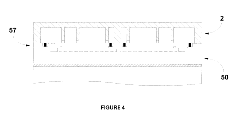
Figure 4 illustrates the structured SOI wafer 50 and the first composite
wafer 2 brought together to form a double-stack wafer 57, which can be
achieved by using anodic bonding to seal a first internal bond interface
between
the second bonding surface of the composite wafer 2 and the patterned surface
of the silicon device layer 1. In the example shown, anodic bonding is
performed
using the contiguous layer of dielectric material 43 provided on the first
composite wafer 2 as the first contacting surface and the handle wafer 51 of
the
SOI wafer 50 as the second contacting surface.
As described above, however, an alternative would be to remove the
contiguous layer of dielectric material 43 and then also partially remove, or
recess, silicon parts 15, 16 to expose part of each dielectric insert 14,
which
would collectively provide the first contacting surface consisting of
dielectric
material. Furthermore, if a single, silicon wafer was being used instead of an
SOI
wafer 50, the second contacting surface could be either the surface of the
second silicon wafer which opposes the first contacting surface of the first
composite wafer, or indeed it could be a side of the second silicon wafer 1
being
attached to the first composite wafer 2.
Figure 5 shows a detailed view of the double-stack bonded wafer 57 after
the first composite wafer 2 and structured SOI wafer 50 have been joined,
illustrating an example of a top side capacitor 59, a top side internal
electrical
contact 21 and a top side stopper 23. The internal electrical contact 21 is
formed
by the thin metal layer 47 provided on the first composite wafer 2 and the
thin
metal layer 53 provided on the structured SOI wafer 50 being squeezed together
during the joining process. To achieve a reliable internal electrical contact,
the
CA 02796552 2012-10-16
WO 2011/128446 PCT/EP2011/056054
8
depth of the first recess 25 and the thickness of the metal layers 47 and 53
must
be chosen with care and optimised to take into account the effect of the
processing tolerances.
Figure 6 illustrates the next step of the fabrication sequence that removes
the excess materials from the double-stack bonded wafer 57 once bonding has
taken place. For example, grinding, followed by CMP, can be used to remove
the contiguous layer of dielectric 43, which acted as the first contacting
surface
for the previous anodic bonding sealing step, thus exposing the silicon
pattern of
the composite wafer 2. Alternatively, the contiguous layer of dielectric 43
may be
left on the first composite wafer 2.
The handle layer 51 of the SOI wafer 50 can also be removed by
grinding, for example, followed by reactive ion etching with etch stop on the
buried oxide layer 52, with etching being used to remove the buried oxide
layer
52 to expose the lower surface of the released silicon device layer 1. An
alternative option, but which is more expensive and time consuming, would be
to
remove the handle wafer 51 by etching only, with etch stop on the buried oxide
layer 52.
Figure 7 illustrates the fabrication sequence that structures the lower
surface of the silicon device layer 1. In this example, a protective metal
layer 61,
such as aluminium, is shown deposited on the upper surface of the double-stack
wafer 57 before the first processing step. The protective metal layer 61 is,
however, optional at this stage and is sometimes used to enhance the gripping
force holding the wafer to electrostatic chucks during subsequent processing.
The first processing step of the double-stack bonded wafer 57 consists in
defining a first, shallow recess 26 serving as requisite spacing for bottom
side
internal electrical contacts, explained further on.
The second processing step consists in defining a second, deeper recess
28 to serve as a capacitance gap for a number of subsequent bottom side
capacitors.
In this example, the first and second recesses 26, 28 provided on the
lower surface of the silicon device layer 1 have the same pattern and depth as
the first and second recesses 25, 27 formed previously on an upper surface of
CA 02796552 2012-10-16
WO 2011/128446 PCT/EP2011/056054
9
the silicon device layer 1, such that the two surfaces are substantially
symmetrical.
The combination of first, shallow recess 26 and second, deeper recess 28
enables the creation of bottom side silicon stoppers 24, at dedicated
locations
within the second recess 28, the stoppers 23 being employed to prevent
stiction
and accidental electrical short-circuiting.
The third processing step consists in depositing and patterning a thin
metal layer 54, such as titanium or aluminium, to form a part of bottom side
internal electrical contacts. The metal layer 54 on the back surface of the
silicon
device layer 1 preferably has the same composition, pattern and thickness as
the metal layer 53 on the upper surface of the silicon device layer 1.
The fourth processing step, in this example, consists of releasing a
portion of the silicon device layer 1 forming the masses and beams by deep
reactive ion etching 56 to provide a double-sided sensor upon which excitation
and detection means may be symmetrically arranged.
Figure 8 shows the double-stack bonded wafer 57 and the second
composite wafer 3 sealed together to form a triple-stack bonded wafer 58,
which
can be achieved using anodic bonding to seal a second internal bond interface
between the second bonding surface of the second composite wafer 3 and the
silicon device layer 1 of the SOI wafer 50. As will be understood from the
preceding description, a preferably, contiguous conductive layer is required
to
provide a first contacting surface on the first and/or second composite wafer
2, 3
for securing a bonding electrode during subsequent anodic bonding. If the
contiguous layer of dielectric 43 is left on the double-stack bonded wafer,
this
can be used as the first contacting surface.
Alternatively, a, preferably, contiguous metal layer 61 may be deposited
on the wafer, as shown in this example of the present invention, wherein
anodic
bonding is achieved using the first contacting surface provided on the first
composite wafer 2 as described above, and the contiguous layer of dielectric
44
provided on the second composite wafer 3 as the second contacting surface.
Alternatively, the contiguous layer of dielectric material 44 may be removed
from
the second composite wafer 3, similar to as described above for the first
composite wafer 2, and the silicon parts 16 may be partially removed, or
CA 02796552 2012-10-16
WO 2011/128446 PCT/EP2011/056054
recessed, to expose part of each dielectric insert 14, which would
collectively
provide the second contacting surface.
Furthermore, it will be recognised that, in the event that the silicon device
layer 1 is a continuous piece of silicon that extends the width of the
composite
5 wafer 2, 3, a bonding electrode may be attached to a side of the silicon
device
layer 1 acting as the first contacting surface instead of the first contacting
surface being provided on the first composite wafer 2, with the second
contacting surface being provided on the second composite wafer 3.
Figure 9 shows a detailed view of the triple-stack bonded wafer 58 after
10 the double-stack bonded wafer 57 and second composite wafer 3 have been
joined together, illustrating an example of a bottom side capacitor 60, a
bottom
side internal electrical contact 22 and a bottom side stopper 24. As with the
top
side electrical contact 21, the bottom side internal electrical contact 22 is
formed
by the thin metal layer 48 provided on the second composite wafer 3 and the
thin
metal layer 54 provided on the silicon device layer 1 being squeezed together
during the joining process. To achieve a reliable internal electrical contact,
the
depth of the lower side shallow recess 26 and the thickness of the metal
layers
48 and 54 must be chosen with care and optimised to take into account the
effect of the processing tolerances.
Figure 10 illustrates the next step of the fabrication sequence that
removes the excess materials from the triple-stack bonded wafer 58. For
instance, grinding, followed by CMP, can be used to remove the contiguous
layer of dielectric 44, which was required in combination with the previous
anodic
bonding sealing technique, thus exposing the silicon pattern of the composite
wafer 3. Dry etching, wet etching, or any other suitable method can be used to
remove the protective metal layer 61, if present.
Figure 11 illustrates the fabrication sequence that creates the external
metallisation on the triple-stack bonded wafer 58. Metal layers, suitable for
forming an electrical contact, are deposited and subsequently patterned on the
upper and lower outer surfaces of the triple-stack bonded wafer 58, to form
the
top side pads 29 and bottom side pads 30. Patterns in the same metal layers
allow direct electrical connection between the pads and the corresponding
CA 02796552 2012-10-16
WO 2011/128446 PCT/EP2011/056054
11
silicon 15, 16 of the composite wafers 2, 3. A suitable singulation method can
then be used to separate the individual chips.
Although other suitable bonding processes, such as, for example, direct
bonding, eutectic bonding, plasma activated and thermo-compression bonding
may be used to join the composite wafer to the structured silicon substrate,
only
anodic bonding creates a hermetic seal at the silicon-dielectric interface in
the
composite wafer. With other bonding methods, the hermeticity inherent between
the silicon-dielectric interfaces in the composite wafer will depend solely on
the
"mechanical fit" provided by the "melt and mould" procedure.
Furthermore, getter material may be applied to any surface inside the
sealed cavity that is formed by the method of the present invention. For
example, getter material may be applied to the first and/or second internal
bonding surfaces of the second silicon wafer and/or the second bonding surface
of either or both the first and second composite wafers 2, 3.
In the above-described example of the present invention, the MEMS
structure comprises both a first composite wafer 2 and a second composite
wafer 3. A skilled person will, of course, recognise that a MEMS structure
having
any number of composite wafers may be produced using the method of the
present invention. For example, if only a single composite wafer is used then
the
lower surface of the silicon wafer 1 may not need to be processed as described
in the above example.