Note: Descriptions are shown in the official language in which they were submitted.
CA 02797486 2012-10-24
WO 2011/139548 PCT/US2011/033015
FLEXIBLE ELECTRICAL CONNECTION OF AN LED-BASED ILLUMINATION
DEVICE TO A LIGHT FIXTURE
Gerard Harbers
Gregory W. Eng
Christopher R. Reed
Peter K. Tseng
John Yriberri
CROSS REFERENCE TO RELATED APPLICATIONS
This application claims priority to Provisional
Application No. 61/331,225, filed May 4, 2010, and US Serial No.
13/089,316, filed April 19, 2011, and US Serial No. 13/089,317,
filed April 19, 2011, all of which are incorporated by reference
herein in their entirety.
TECHNICAL FIELD
The described embodiments relate to illumination devices
that include Light Emitting Diodes (LEDs).
BACKGROUND INFORMATION
The use of LEDs in general lighting is becoming more
desirable and more prevalent. Illumination devices that include
LEDs typically require large amounts of heat sinking and
specific power requirements. Consequently, many such
illumination devices must be mounted to light fixtures that
include heat sinks and provide the necessary power. The
typically electrical connection of such an LED illumination
device to a light fixture, unfortunately, is not user friendly.
Consequently, improvements are desired.
Summary
In accordance with one embodiment, an electrical
interface module is provided between an LED illumination device
and a light fixture. The electrical interface module includes
1
CA 02797486 2012-10-24
WO 2011/139548 PCT/US2011/033015
an arrangement of electrical contact surfaces that are adapted
to be coupled to an LED illumination device and a second
arrangement of electrical contact surfaces that are adapted to
be coupled to the light fixture. The electrical contact
surfaces may be adapted to be electrically coupleable to
different configurations of contact surfaces on different LED
illumination devices. The electrical interface module may
include a power converter that is coupled to the LED
illumination device through the electrical contact surfaces.
Additionally, an LED selection module that uses switching
elements to selectively turn on or off LEDs in the LED
illumination device. A communication port that is controlled by
a processor may be included to transmit information associated
with the LED illumination device, such as identification,
indication of lifetime, flux, etc. The lifetime of the LED
illumination device may be measured by accumulating the number
of cycles generated by an electronic circuit and communicated,
e.g., by an RF signal, IR signal, wired signal or by controlling
the light output of the LED illumination device. Additionally,
an optic that is replaceably mounted to the LED illumination
device may include, e.g., a flux sensor that is connected to the
electrical interface.
BRIEF DESCRIPTION OF THE DRAWINGS
Figs. 1-2 illustrate two exemplary luminaires, including
an illumination device, reflector, and light fixture.
Fig. 3A shows an exploded view illustrating components of
LED based illumination device as depicted in Fig. 1.
Fig. 3B illustrates a perspective, cross-sectional view
of LED based illumination device as depicted in Fig. 1.
Fig. 4 illustrates a cut-away view of luminaire as
depicted in Fig. 2, with an electrical interface module coupled
between the LED illumination device and the light fixture.
Figs. 5A-5B illustrate two different configurations of
the electrical interface module.
2
CA 02797486 2012-10-24
WO 2011/139548 PCT/US2011/033015
Figs. 6A-6B illustrate selectively masking and exposing
terminal locations on the electrical interface module.
Fig. 7 illustrates a lead frame that may be used to
position a plurality of spring pins for contact with the
electrical interface module.
Fig. 8 illustrates an embodiment of the spring pins that
may be used to contact the electrical interface module.
Figs. 9A-9C illustrate a plurality of radially spaced
electrical contacts that may be used with the electrical
interface module.
Fig. 10 is a schematic diagram illustrative of the
electrical interface module in greater detail.
Fig. 11 is a schematic illustrative of an LED selection
module.
Fig. 12 is a graph illustrative of selecting LEDs to
change the amount of flux emitted by powered LEDs.
Fig. 13 is a flow chart illustrating a process of
externally communicating LED illumination device information.
Fig. 14 illustrates an optic in the form of a reflector
that includes at least one sensor that is in electrical contact
with the electrical interface module.
Fig. 15 is illustrative of locations on the reflector
sensors may be positioned.
DETAILED DESCRIPTION
Reference will now be made in detail to background
examples and some embodiments of the invention, examples of
which are illustrated in the accompanying drawings.
Figs. 1-2 illustrate two exemplary luminaires. The
luminaire illustrated in Fig. 1 includes an illumination device
100 with a rectangular form factor. The luminaire illustrated
in Fig. 2 includes an illumination device 100 with a circular
form factor. These examples are for illustrative purposes.
Examples of illumination devices of general polygonal and
elliptical shapes may also be contemplated. Luminaire 150
3
CA 02797486 2012-10-24
WO 2011/139548 PCT/US2011/033015
includes illumination device 100, reflector 140, and light
fixture 130. As depicted, light fixture 130 is a heat sink, and
thus, may sometimes be referred as heat sink 130. However,
light fixture 130 may include other structural and decorative
elements (not shown). Reflector 140 is mounted to illumination
device 100 to collimate or deflect light emitted from
illumination device 100. The reflector 140 may be made from a
thermally conductive material, such as a material that includes
aluminum or copper and may be thermally coupled to illumination
device 100. Heat flows by conduction through illumination
device 100 and the thermally conductive reflector 140. Heat
also flows via thermal convection over the reflector 140.
Reflector 140 may be a compound parabolic concentrator, where
the concentrator is constructed of or coated with a highly
reflecting material. Compound parabolic concentrators tend to
be tall, but they often are used in a reduced length form, which
increases the beam angle. An advantage of this configuration is
that no additional diffusers are required to homogenize the
light, which increases the throughput efficiency. Optical
elements, such as a diffuser or reflector 140 may be removably
coupled to illumination device 100, e.g., by means of threads, a
clamp, a twist-lock mechanism, or other appropriate arrangement.
Illumination device 100 is mounted to light fixture 130.
As depicted in Figs. 1 and 2, illumination device 100 is mounted
to heat sink 130. Heat sink 130 may be made from a thermally
conductive material, such as a material that includes aluminum
or copper and may be thermally coupled to illumination device
100. Heat flows by conduction through illumination device 100
and the thermally conductive heat sink 130. Heat also flows via
thermal convection over heat sink 130. Illumination device 100
may be attached to heat sink 130 by way of screw threads to
clamp the illumination device 100 to the heat sink 130. To
facilitate easy removal and replacement of illumination device
100, illumination device 100 may be removably coupled to heat
sink 130, e.g., by means of a clamp mechanism, a twist-lock
4
CA 02797486 2012-10-24
WO 2011/139548 PCT/US2011/033015
mechanism, or other appropriate arrangement. Illumination
device 100 includes at least one thermally conductive surface
that is thermally coupled to heat sink 130, e.g., directly or
using thermal grease, thermal tape, thermal pads, or thermal
epoxy. For adequate cooling of the LEDs, a thermal contact area
of at least 50 square millimeters, but preferably 100 square
millimeters should be used per one watt of electrical energy
flow into the LEDs on the board. For example, in the case when
20 LEDs are used, a 1000 to 2000 square millimeter heatsink
contact area should be used. Using a larger heat sink 130 may
permit the LEDs 102 to be driven at higher power, and also
allows for different heat sink designs. For example, some
designs may exhibit a cooling capacity that is less dependent on
the orientation of the heat sink. In addition, fans or other
solutions for forced cooling may be used to remove the heat from
the device. The bottom heat sink may include an aperture so
that electrical connections can be made to the illumination
device 100.
Fig. 3A shows an exploded view illustrating components
of LED illumination device 100 as depicted in Fig. 1. It should
be understood that as defined herein an LED illumination device
is not an LED, but is an LED light source or fixture or
component part of an LED light source or fixture. LED
illumination device 100 includes one or more LED die or packaged
LEDs and a mounting board to which LED die or packaged LEDs are
attached. Fig. 3B illustrates a perspective, cross-sectional
view of LED illumination device 100 as depicted in Fig. 1. LED
illumination device 100 includes one or more solid state light
emitting elements, such as light emitting diodes (LEDs) 102,
mounted on mounting board 104. Mounting board 104 is attached
to mounting base 101 and secured in position by mounting board
retaining ring 103. Together, mounting board 104 populated by
LEDs 102 and mounting board retaining ring 103 comprise light
source sub-assembly 115. Light source sub-assembly 115 is
operable to convert electrical energy into light using LEDs 102.
5
CA 02797486 2012-10-24
WO 2011/139548 PCT/US2011/033015
The light emitted from light source sub-assembly 115 is directed
to light conversion sub-assembly 116 for color mixing and color
conversion. Light conversion sub-assembly 116 includes cavity
body 105 and output window 108, and optionally includes either
or both bottom reflector insert 106 and sidewall insert 107.
Output window 108 is fixed to the top of cavity body 105.
Cavity body 105 includes interior sidewalls such that the
interior sidewalls direct light from the LEDs 102 to the output
window 108 when cavity body 105 is mounted over light source
sub-assembly 115. Bottom reflector insert 106 may optionally be
placed over mounting board 104. Bottom reflector insert 106
includes holes such that the light emitting portion of each LED
102 is not blocked by bottom reflector insert 106. Sidewall
insert 107 may optionally be placed inside cavity body 105 such
that the interior surfaces of sidewall insert 107 direct light
from the LEDs 102 to the output window when cavity body 105 is
mounted over light source sub-assembly 115. Although as
depicted, the interior sidewalls of cavity body 105 are
rectangular in shape as viewed from the top of illumination
device 100, other shapes may be contemplated (e.g. clover shaped
or polygonal). In addition, the interior sidewalls of cavity
body 105 may taper outward from mounting board 104 to output
window 108, rather than perpendicular to output window 108 as
depicted.
In this embodiment, the sidewall insert 107, output
window 108, and bottom reflector insert 106 disposed on mounting
board 104 define a light mixing cavity 109 in the LED
illumination device 100 in which a portion of light from the
LEDs 102 is reflected until it exits through output window 108.
Reflecting the light within the cavity 109 prior to exiting the
output window 108 has the effect of mixing the light and
providing a more uniform distribution of the light that is
emitted from the LED illumination device 100. Portions of
sidewall insert 107 may be coated with a wavelength converting
material. Furthermore, portions of output window 108 may be
6
CA 02797486 2012-10-24
WO 2011/139548 PCT/US2011/033015
coated with the same or a different wavelength converting
material. In addition, portions of bottom reflector insert 106
may be coated with the same or a different wavelength converting
material. The photo converting properties of these materials in
combination with the mixing of light within cavity 109 results
in a color converted light output by output window 108. By
tuning the chemical properties of the wavelength converting
materials and the geometric properties of the coatings on the
interior surfaces of cavity 109, specific color properties of
light output by output window 108 may be specified, e.g. color
point, color temperature, and color rendering index (CRI).
For purposes of this patent document, a wavelength
converting material is any single chemical compound or mixture
of different chemical compounds that performs a color conversion
function, e.g. absorbs light of one peak wavelength and emits
light at another peak wavelength.
Cavity 109 may be filled with a non-solid material, such
as air or an inert gas, so that the LEDs 102 emit light into the
non-solid material. By way of example, the cavity may be
hermetically sealed and Argon gas used to fill the cavity.
Alternatively, Nitrogen may be used. In other embodiments,
cavity 109 may be filled with a solid encapsulent material. By
way of example, silicone may be used to fill the cavity.
The LEDs 102 can emit different or the same colors,
either by direct emission or by phosphor conversion, e.g., where
phosphor layers are applied to the LEDs as part of the LED
package. Thus, the illumination device 100 may use any
combination of colored LEDs 102, such as red, green, blue,
amber, or cyan, or the LEDs 102 may all produce the same color
light or may all produce white light. For example, the LEDs 102
may all emit either blue or UV light. When used in combination
with phosphors (or other wavelength conversion means), which may
be, e.g., in or on the output window 108, applied to the
sidewalls of cavity body 105, or applied to other components
7
CA 02797486 2012-10-24
WO 2011/139548 PCT/US2011/033015
placed inside the cavity (not shown), such that the output light
of the illumination device 100 has the color as desired.
The mounting board 104 provides electrical connections
to the attached LEDs 102 to a power supply (not shown). In one
embodiment, the LEDs 102 are packaged LEDs, such as the Luxeon
Rebel manufactured by Philips Lumileds Lighting. Other types of
packaged LEDs may also be used, such as those manufactured by
OSRAM (Ostar package), Luminus Devices (USA), Cree (USA), Nichia
(Japan), or Tridonic (Austria). As defined herein, a packaged
LED is an assembly of one or more LED die that contains
electrical connections, such as wire bond connections or stud
bumps, and possibly includes an optical element and thermal,
mechanical, and electrical interfaces. The LEDs 102 may include
a lens over the LED chips. Alternatively, LEDs without a lens
may be used. LEDs without lenses may include protective layers,
which may include phosphors. The phosphors can be applied as a
dispersion in a binder, or applied as a separate plate. Each
LED 102 includes at least one LED chip or die, which may be
mounted on a submount. The LED chip typically has a size about
lmm by lmm by 0.5mm, but these dimensions may vary. In some
embodiments, the LEDs 102 may include multiple chips. The
multiple chips can emit light similar or different colors, e.g.,
red, green, and blue. The LEDs 102 may emit polarized light or
non-polarized light and LED based illumination device 100 may
use any combination of polarized or non-polarized LEDs. In some
embodiments, LEDs 102 emit either blue or UV light because of
the efficiency of LEDs emitting in these wavelength ranges. In
addition, different phosphor layers may be applied on different
chips on the same submount. The submount may be ceramic or
other appropriate material. The submount typically includes
electrical contact pads on a bottom surface that are coupled to
contacts on the mounting board 104. Alternatively, electrical
bond wires may be used to electrically connect the chips to a
mounting board. Along with electrical contact pads, the LEDs
102 may include thermal contact areas on the bottom surface of
8
CA 02797486 2012-10-24
WO 2011/139548 PCT/US2011/033015
the submount through which heat generated by the LED chips can
be extracted. The thermal contact areas are coupled to heat
spreading layers on the mounting board 104. Heat spreading
layers may be disposed on any of the top, bottom, or
intermediate layers of mounting board 104. Heat spreading
layers may be connected by vias that connect any of the top,
bottom, and intermediate heat spreading layers.
In some embodiments, the mounting board 104 conducts
heat generated by the LEDs 102 to the sides of the board 104 and
the bottom of the board 104. In one example, the bottom of
mounting board 104 may be thermally coupled to a heat sink 130
(shown in Figs. 1 and 2) via mounting base 101. In other
examples, mounting board 104 may be directly coupled to a heat
sink, or a lighting fixture and/or other mechanisms to dissipate
the heat, such as a fan. In some embodiments, the mounting
board 104 conducts heat to a heat sink thermally coupled to the
top of the board 104. For example, mounting board retaining
ring 103 and cavity body 105 may conduct heat away from the top
surface of mounting board 104. Mounting board 104 may be an FR4
board, e.g., that is 0.5mm thick, with relatively thick copper
layers, e.g., 30 m to 100 m, on the top and bottom surfaces that
serve as thermal contact areas. In other examples, the board
104 may be a metal core printed circuit board (PCB) or a ceramic
submount with appropriate electrical connections. Other types
of boards may be used, such as those made of alumina (aluminum
oxide in ceramic form), or aluminum nitride (also in ceramic
form).
Mounting board 104 includes electrical pads to which the
electrical pads on the LEDs 102 are connected. The electrical
pads are electrically connected by a metal, e.g., copper, trace
to a contact, to which a wire, bridge or other external
electrical source is connected. In some embodiments, the
electrical pads may be vias through the board 104 and the
electrical connection is made on the opposite side, i.e., the
bottom, of the board. Mounting board 104, as illustrated, is
9
CA 02797486 2012-10-24
WO 2011/139548 PCT/US2011/033015
rectangular in dimension. LEDs 102 mounted to mounting board
104 may be arranged in different configurations on rectangular
mounting board 104. In one example LEDs 102 are aligned in rows
extending in the length dimension and in columns extending in
the width dimension of mounting board 104. In another example,
LEDs 102 are arranged in a hexagonally closely packed structure.
In such an arrangement each LED is equidistant from each of its
immediate neighbors. Such an arrangement is desirable to
increase the uniformity and efficiency of light emitted from the
light source sub-assembly 115.
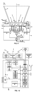
Fig. 4 illustrates a cut-away view of luminaire 150 as
depicted in Fig. 2. Reflector 140 is removably coupled to
illumination device 100. Reflector 140 is coupled to
illumination device 100 by a twist-lock mechanism. Reflector
140 is aligned with illumination device 100 by bringing
reflector 140 into contact with illumination device 100 through
openings in reflector retaining ring 110. Reflector 140 is
coupled to illumination device 100 by rotating reflector 140
about optical axis (OA) to an engaged position. In the engaged
position, the reflector 140 is captured between mounting board
retaining ring 103 and reflector retaining ring 110. In the
engaged position, an interface pressure may be generated between
mating thermal interface surface 140surface of reflector 140 and
mounting board retaining ring 103. In this manner, heat
generated by LEDs 102 may be conducted via mounting board 104,
through mounting board retaining ring 103, through interface
140surface. and into reflector 140. In addition, a plurality of
electrical connections may be formed between reflector 140 and
retaining ring 103.
Illumination device 100 includes an electrical interface
module (EIM) 120. As illustrated, EIM 120 may be removably
attached to illumination device 100 by retaining clips 137. In
other embodiments, EIM 120 may be removably attached to
illumination device 100 by an electrical connector coupling EIM
120 to mounting board 104. EIM 120 may also be coupled to
CA 02797486 2012-10-24
WO 2011/139548 PCT/US2011/033015
illumination device 100 by other fastening means, e.g. screw
fasteners, rivets, or snap-fit connectors. As depicted EIM 120
is positioned within a cavity of illumination device 100. In
this manner, EIM 120 is contained within illumination device 100
and is accessible from the bottom side of illumination device
100. In other embodiments, EIM 120 may be at least partially
positioned within light fixture 130. The EIM 120 communicates
electrical signals from light fixture 130 to illumination device
100. Electrical conductors 132 are coupled to light fixture 130
at electrical connector 133. By way of example, electrical
connector 133 may be a registered jack (RJ) connector commonly
used in network communications applications. In other examples,
electrical conductors 132 may be coupled to light fixture 130 by
screws or clamps. In other examples, electrical conductors 132
may be coupled to light fixture 130 by a removable slip-fit
electrical connector. Connector 133 is coupled to conductors
134. Conductors 134 are removably coupled to electrical
connector 121 mounted to EIM 120. Similarly, electrical
connector 121 may be a RJ connector or any suitable removable
electrical connector. Connector 121 is fixedly coupled to EIM
120. Electrical signals 135 are communicated over conductors
132 through electrical connector 133, over conductors 134,
through electrical connector 121 to EIM 120. Electrical signals
135 may include power signals and data signals. EIM 120 routes
electrical signals 135 from electrical connector 121 to
appropriate electrical contact pads on EIM 120. For example,
conductor 139 within EIM 120 may couple connector 121 to
electrical contact pad 170 on the top surface of EIM 120.
Alternatively, connector 121 may be mounted on the same side of
EIM 120 as the electrical contact pads 170, and thus, a surface
conductor may couple connector 121 to the electrical contact
pads 170. As illustrated, spring pin 122 removably couples
electrical contact pad 170 to mounting board 104 through an
aperture 138 in mounting base 101. Spring pins couple contact
pads disposed on the top surface of EIM 120 to contact pads of
11
CA 02797486 2012-10-24
WO 2011/139548 PCT/US2011/033015
mounting board 104. In this manner, electrical signals are
communicated from EIM 120 to mounting board 104. Mounting board
104 includes conductors to appropriately couple LEDs 102 to the
contact pads of mounting board 104. In this manner, electrical
signals are communicated from mounting board 104 to appropriate
LEDs 102 to generate light. EIM 120 may be constructed from a
printed circuit board (PCB), a metal core PCB, a ceramic
substrate, or a semiconductor substrate. Other types of boards
may be used, such as those made of alumina (aluminum oxide in
ceramic form), or aluminum nitride (also in ceramic form). EIM
120 may be a constructed as a plastic part including a plurality
of insert molded metal conductors.
Mounting base 101 is replaceably coupled to light
fixture 130. In the illustrated example, light fixture 130 acts
as a heat sink. Mounting base 101 and light fixture 130 are
coupled together at a thermal interface 136. At the thermal
interface 136, a portion of mounting base 101 and a portion of
light fixture 130 are brought into contact as illumination
device 100 is coupled to light fixture 130. In this manner,
heat generated by LEDs 102 may be conducted via mounting board
104, through mounting base 101, through interface 136, and into
light fixture 130.
To remove and replace illumination device 100,
illumination device 100 is decoupled from light fixture 130 and
electrical connector 121 is disconnected. In one example,
conductors 134 includes sufficient length to allow sufficient
separation between illumination device 100 and light fixture 130
to allow an operator to reach between fixture 130 and
illumination device 100 to disconnect connector 121. In another
example, connector 121 may be arranged such that a displacement
between illumination device 100 from light fixture 130 operates
to disconnect connector 121. In another example, conductors 134
are wound around a spring-loaded reel. In this manner,
conductors 134 may be extended by unwinding from the reel to
allow for connection or disconnection of connector 121, and then
12
CA 02797486 2012-10-24
WO 2011/139548 PCT/US2011/033015
conductors 134 may be retracted by winding conductors 134 onto
the reel by action of spring-loaded reel.
Figs. 5A-B illustrate EIM 120 coupled to mounting board
104 in two different configurations. As illustrated in Fig. 5A,
mounting board 104 is coupled to EIM 120 by spring pin assembly
123 in a first configuration. EIM 120 includes conductors 124
and 125. Electrical signal 126 is communicated from connector
121, over conductor 124, over spring pin assembly 123 in a first
configuration to terminal 128 of mounting board 104. Electrical
signal 127 is communicated from terminal 129 of mounting board
104, over spring pin assembly 123 in a first configuration, over
conductor 125, to connector 121. As illustrated in Fig. 5B,
mounting board 104 is coupled to EIM 120 by spring pin assembly
123 in a second configuration. Electrical signal 126 is
communicated from connector 121, over conductor 124, over spring
pin assembly 123 in the second configuration to terminal 141 of
mounting board 104. Electrical signal 127 is communicated from
terminal 142 of mounting board 104, over spring pin assembly 123
in a second configuration, over conductor 125, to connector 121.
As illustrated in Figs. 5A-B, the same EIM 120 may communicate
electrical signals to mounting boards with different terminal
locations. Conductors 124 and 125 are configured such that the
same signal from connector 121 can be communicated between
multiple terminals at the interface between EIM 120 and spring
pin assembly 123. Different configurations of spring pin
assembly 123 can be utilized to communicate signals to different
terminal locations of mounting board 104. In this manner, the
same connector 121 and EIM 120 may be utilized to address a
variety of different terminal configurations of mounting boards
within illumination device 100.
In other embodiments, the same spring pin assembly 123,
connector 121, and EIM 120 may be utilized to address a variety
of different terminal configurations of mounting boards within
illumination device 100. As illustrated in Figs. 6A-B, by
selectively masking and exposing terminal locations on the
13
CA 02797486 2012-10-24
WO 2011/139548 PCT/US2011/033015
surface of mounting board 104, different terminals of mounting
board 104 may be coupled to spring pin assembly 123. As
discussed above with respect to Figs. 5A and 5B, EIM 120 may
supply electrical signals to mounting boards of different
physical configurations. Conductors 124 and 125 are configured
such that a signal from connector 121 can be communicated to
multiple terminals at the interface between EIM 120 and spring
pin assembly 123. In this manner, the same connector 121, EIM
120, and spring pin assembly 123 may be utilized to address a
variety of different terminal configurations of mounting boards
within illumination device 100 by selectively masking and
exposing terminal locations on the surface of mounting board
104, illustrated in Fig. 6A as masked terminal 142MASKED and
exposed terminal 129EXPOSED and illustrated in Fig. 6B exposed
terminal 142EXPOSED and masked terminal 129MAsKED-
As depicted in Figs. 4 and 6A, 6B, spring pin assembly
123 includes a plurality of spring pins. As depicted in Fig. 7,
the plurality of spring pins in the spring pin assembly 123 may
be positioned with respect to one another by a lead frame 143.
In other embodiments, the plurality of spring pins may be molded
in with frame 143 to generate molded-in lead frame 143. The
lead frame 143 may be connected to EIM 120 or to mounting base
101. Spring pin 122 may be shaped such that the spring pin 122
is compliant along the axis of the pin, as depicted in Fig. 4.
For example, pin 122 includes a hook shape at one end that
serves to make contact with a terminal, but also serves to
displace when a force is applied between the two ends of the
pin. The compliance of each pin of spring pin assembly 123
ensures that each pin makes contact with terminals on each end
of each pin when EIM 120 and mounting board 104 are brought into
electrical contact. In other embodiments, spring pin 122 may
include multiple parts to achieve compliance along the axial
direction of pin 122 as illustrated in Fig. 8. Electrical
contact between each spring pin and EIM 120 may be made at the
14
CA 02797486 2012-10-24
WO 2011/139548 PCT/US2011/033015
top surface of EIM 120, but may also be made at the bottom
surface.
Although, as depicted in Fig. 4, a RJ connector is
employed to couple light fixture 130 to EIM 120, other connector
configurations may be contemplated. In some embodiments, a slip
connector may be employed to electrically couple EIM 120 to
fixture 130. In other embodiments, a plurality of radially
spaced electrical contacts may be employed. For example, Figs.
9A-C illustrate an embodiment that employs a plurality of
radially spaced electrical contacts. Fig. 9A illustrates a side
view of light fixture 130 and EIM 120. Fig. 9B illustrates a
bottom view of EIM 120. EIM 120 includes a plurality of
radially spaced electrical contacts 152. As depicted,
electrical contacts 152 are circular shaped, but other
elliptical or polygonal shapes may be contemplated. When EIM
120 is coupled to light fixture 130, contacts 152 align and make
contact with spring contacts 151 of light fixture 130. Fig. 9C
illustrates a top view of light fixture 130 including spring
contacts 151. In the depicted configuration, EIM 120 may be
aligned with light fixture 130 and make electrical contact with
fixture 130 regardless of the orientation of EIM 120 with
respect to fixture 130. In other examples, an alignment feature
may be utilized to align EIM 120 with light fixture 130 in a
predetermined orientation.
Fig. 10 is a schematic diagram illustrative of EIM 120
in greater detail. In the depicted embodiment, EIM 120 includes
bus 21, powered device interface controller (PDIC) 34, processor
22, elapsed time counter module (ETCM) 27, an amount of non-
volatile memory 26 (e.g. EPROM), an amount of non-volatile
memory 23 (e.g. flash memory), infrared transceiver 25, RF
transceiver 24, sensor interface 28, power converter interface
29, power converter 30, and LED selection module 40. LED
mounting board 104 is coupled to EIM 120. LED mounting board
104 includes flux sensor 36, LED circuitry 33 including LEDs
102, and temperature sensor 31. EIM 120 is also coupled to flux
CA 02797486 2012-10-24
WO 2011/139548 PCT/US2011/033015
sensor 32 and occupancy sensor 35 mounted to light fixture 130.
In some embodiments, flux sensor 32 and occupancy sensor 35 may
be mounted to an optic, such as reflector 140 as discussed with
respect to Fig. 14. In some embodiments, an occupancy sensor
may also be mounted to mounting board 104. In some embodiments,
any of an accelerometer, a pressure sensor, and a humidity
sensor may be mounted to mounting board 104. For example, an
accelerometer may be added to detect the orientation of
illumination device 100 with respect to the gravitational field.
In another example, the accelerometer may provide a measure of
vibration present in the operating environment of illumination
device 100. In another example, a humidity sensor may be added
to provide a measure of the moisture content of the operating
environment of illumination device 100. For example, if
illumination device 100 is sealed to reliably operate in wet
conditions, the humidity sensor may be employed to detect a
failure of the seal and contamination of the illumination
device. In another example, a pressure sensor may be employed
to provide a measure of the pressure of the operating
environment of illumination device 100. For example, if
illumination device 100 is sealed and evacuated, or
alternatively, sealed and pressurized, the pressure sensor may
be employed to detect a failure of the seal.
PDIC 34 is coupled to connector 121 and receives
electrical signals 135 over conductors 134. In one example,
PDIC 34 is a device complying with the IEEE 802.3 protocol for
transmitting power and data signals over multi-conductor cabling
(e.g. category 5e cable). PDIC 34 separates incoming signals
135 into data signals 41 communicated to bus 21 and power
signals 42 communicated to power converter 30 in accordance with
the IEEE 802.3 protocol. Power converter 30 operates to perform
power conversion to generate electrical signals to drive one or
more LED circuits of circuitry 33. In some embodiments, power
converter 30 operates in a current control mode to supply a
controlled amount of current to LED circuits within a predefined
16
CA 02797486 2012-10-24
WO 2011/139548 PCT/US2011/033015
voltage range. In some embodiments, power converter 30 is a
direct current to direct current (DC-DC) power converter. In
these embodiments, power signals 42 may have a nominal voltage
of 48 volts in accordance with the IEEE 802.3 standard. Power
signals 42 are stepped down in voltage by DC-DC power converter
30 to voltage levels that meet the voltage requirements of each
LED circuit coupled to DC-DC converter 30.
In some other embodiments, power converter 30 is an
alternating current to direct current (AC-DC) power converter.
In yet other embodiments, power converter 30 is an alternating
current to alternating current (AC-AC) power converter. In
embodiments employing AC-AC power converter 30, LEDs 102 mounted
to mounting board 104 generate light from AC electrical signals.
Power converter 30 may be single channel or multi-channel. Each
channel of power converter 30 supplies electrical power to one
LED circuit of series connected LEDs. In one embodiment power
converter 30 operates in a constant current mode. This is
particularly useful where LEDs are electrically connected in
series. In some other embodiments, power converter 30 may
operate as a constant voltage source. This may be particularly
useful where LEDs are electrically connected in parallel.
As depicted, power converter 30 is coupled to power
converter interface 29. In this embodiment, power converter
interface 29 includes a digital to analog (D/A) capability.
Digital commands may be generated by operation of processor 22
and communicated to power converter interface 29 over bus 21.
Interface 29 converts the digital command signals to analog
signals and communicates the resulting analog signals to power
converter 30. Power converter 30 adjusts the current
communicated to coupled LED circuits in response to the received
analog signals. In some examples, power converter 30 may shut
down in response to the received signals. In other examples,
power converter 30 may pulse or modulate the current
communicated to coupled LED circuits in response to the received
analog signals. In some embodiments, power converter 30 is
17
CA 02797486 2012-10-24
WO 2011/139548 PCT/US2011/033015
operable to receive digital command signals directly. In these
embodiments, power converter interface 29 is not implemented.
In some embodiments, power converter 30 is operable to transmit
signals. For example, power converter 30 may transmit a signal
indicating a power failure condition or power out of regulation
condition through power converter interface 29 to bus 21.
EIM 120 includes several mechanisms for receiving data
from and transmitting data to devices communicatively linked to
illumination device 100. EIM 120 may receive and transmit data
over PDIC 34, RF transceiver 24, and IR transceiver 25. In
addition, EIM 120 may broadcast data by controlling the light
output from illumination device 100. For example, processor 22
may command the current supplied by power converter 30 to
periodically flash, or otherwise modulate in frequency or
amplitude, the light output of LED circuitry 33. The pulses may
be detectable by humans, e.g. flashing the light output by
illumination device 100 in a sequence of three, one second
pulses, every minute. The pulses may also be undetectable by
humans, but detectable by a flux detector, e.g. pulsing the
light output by illumination device 100 at one kilohertz. In
these embodiments, the light output of illumination device 100
can be modulated to indicate a code. Examples of information
transmitted by EIM 120 by any of the above-mentioned means
includes accumulated elapsed time of illumination device 100,
LED failure, serial number, occupancy sensed by occupancy sensor
35, flux sensed by on-board flux sensor 36, flux sensed by flux
sensor 32, and temperature sensed by temperature sensor 31, and
power failure condition. In addition, EIM 120 may receive
messages by sensing a modulation or cycling of electrical
signals supplying power to illumination device 100. For
example, power line voltage may be cycled three times in one
minute to indicate a request for illumination device 100 to
communicate its serial number.
Fig. 11 is a schematic illustrative of LED selection
module 40 in greater detail. As depicted, LED circuitry 33
18
CA 02797486 2012-10-24
WO 2011/139548 PCT/US2011/033015
includes LEDs 55-59 connected in series and coupled to LED
selection module 140. Although LED circuit 33 includes five
series connected LEDs, more or less LEDs may be contemplated.
In addition, LED board 104 may include more than one circuit of
series connected LEDs. As depicted, LED selection module 40
includes five series connected switching elements 44-48. Each
lead of a switching element is coupled to a corresponding lead
of an LED of LED circuit 33. For example, a first lead of
switching element 44 is coupled to the anode of LED 55 at
voltage node 49. In addition, a second lead of switching
element 44 is coupled to the cathode of LED 55 at voltage node
50. In a similar manner switching elements 45-48 are coupled to
LEDs 55-58 respectively. In addition, an output channel of
power converter 30 is coupled between voltage nodes 49 and 54
forming a current loop 61 conducting current 60. In some
embodiments, switching elements 44-48 may be transistors (e.g.
bipolar junction transistors or field effect transistors).
LED selection module 40 selectively powers LEDs of an
LED circuit 33 coupled to a channel of power converter 30. For
example, in an open position, switching element 44 conducts
substantially no current between voltage nodes 49 and 50. In
this manner, current 60 flowing from voltage node 49 to voltage
node 50 passes through LED 55. In this case, LED 55 offers a
conduction path of substantially lower resistance than switching
element 44, thus current passes through LED 55 and light is
generated. In this way switching element 44 acts to "switch on"
LED 55. By way of example, in a closed position, switching
element 47 is substantially conductive. Current 60 flows from
voltage node 52 to node 53 through switching element 47. In
this case, switching element 47 offers a conduction path of
substantially lower resistance than LED 57, thus current 60
passes through switching element 47, rather than LED 57, and LED
57 does not generate light. In this way switching element 47
acts to "switch off" LED 58. In the described manner, switching
elements 44-48 may selectively power LEDs 55-59.
19
CA 02797486 2012-10-24
WO 2011/139548 PCT/US2011/033015
A binary control signal SEL[5:1] is received onto LED
selection module 40. Control signal SEL[5:1] controls the state
of each of switching elements 44-48, and thus determines whether
each of LEDs 55-59 is "switched on" or "switched off." In one
embodiment, control signal, SEL, is generated by processor 22 in
response to a condition detected by EIM 120 (e.g. reduction in
flux sensed by flux sensor 36). In other embodiments, control
signal, SEL, is generated by processor 22 in response to a
command signal received onto EIM 120 (e.g. communication
received by RF transceiver 24, IR transceiver 25, or PDIC 34).
In another embodiment, the control signal, SEL, is communicated
from an on-board controller of the LED illumination device.
Fig. 12 is illustrative of how LEDs may be switched on
or off to change the amount of flux emitted by powered LEDs of
LED circuit 33. Current 60 is plotted against the luminous flux
emitted by powered LEDs of LED circuit 33. Due to physical
limitations of LEDs 55-59, current 60 is limited to a maximum
current level, Imax, above which lifetime becomes severely
limited. In one example, Imax, may be 0.7 Ampere. In general
LEDs 55-59 exhibit a linear relationship between luminous flux
and drive current. Fig. 12 illustrates luminous flux emitted as
a function of drive current for four cases: when one LED is
"switched on", when two LEDs are "switched on", when three LEDs
are "switched on", and when four LEDs are "switched on". In one
example, a luminous output, L3, may be achieved by switching on
three LEDs and driving them at Imax. Alternatively, luminous
output, L3, may be achieved by switching on four LEDs and driving
them with less current. When reduced amounts of light are
required for a period of time (e.g. dimming of restaurant
lighting), light selection module 40 may be used to selectively
"switch off" LEDs, rather than simply scaling back current.
This may be desirable to increase the lifetime of "switched off"
LEDs in light fixture by not operating them for selected
periods. The LEDs selected to be "switched off" may be
scheduled such that each LED is "switched off" for approximately
CA 02797486 2012-10-24
WO 2011/139548 PCT/US2011/033015
the same amount of time as the others. In this way, the
lifetime of illumination device 100 may be extended by extending
the life of each LED by approximately the same amount of time.
LEDs 55-59 may be selectively switched on or off to
respond to an LED failure. In one embodiment, illumination
device 100 includes extra LEDs that are "switched off."
However, when an LED failure occurs, one or more of the extra
LEDs are "switched on" to compensate for the failed LED. In
another example, extra LEDs may be "switched on" to provide
additional light output. This may be desirable when the
required luminous output of illumination device 100 is not known
prior to installation or when illumination requirements change
after installation.
Fig. 13 is a flow chart illustrating a process of
externally communicating LED illumination device information.
As illustrated, information associated with the LED illumination
device is stored locally, e.g., in non-volatile memory 23 and/or
26 (202). The information, by way of example, may be a LED
illumination device identifier such as a serial number, or
information related to parameters, such as lifetime, flux,
occupancy, LED or power failure conditions, temperature, or any
other desired parameter. In some instances, the information is
measured, such as lifetime, flux, or temperature, while in other
instances, the information need not be measured, such as an
illumination device identifier or configuration information. A
request for information is received (204), e.g., by RF
transceiver 24, IR transceiver, a wired connection, or cycling
the power line voltage. The LED illumination device information
is communicated (206), e.g., by RF transceiver 24, IR
transceiver, a wired connection, or by controlling the light
output from illumination device 100.
EIM 120 stores a serial number that individually
identifies the illumination device 100 to which EIM 120 is a
part. The serial number is stored in non-volatile memory 26 of
EIM 120. In one example, non-volatile memory 26 is an erasable
21
CA 02797486 2012-10-24
WO 2011/139548 PCT/US2011/033015
programmable read-only memory (EPROM). A serial number that
identifies illumination device 100 is programmed into EPROM 26
during manufacture. EIM 120 may communicate the serial number
in response to receiving a request to transmit the serial number
(e.g. communication received by RF transceiver 24, IR
transceiver 25, or PDIC 34). For example, a request for
communication of the illumination device serial number is
received onto EIM 120 (e.g. communication received by RF
transceiver 24, IR transceiver 25, or PDIC 34). In response,
processor 22 reads the serial number stored in memory 26, and
communicates the serial number to any of RF transceiver 24, IR
transceiver 25, or PDIC 34 for communication of the serial
number from EIM 120.
EIM 120 includes temperature measurement, recording, and
communication functionality. At power-up of illumination device
100, sensor interface 28 receives temperature measurements from
temperature sensor 31. Processor 22 periodically reads a
current temperature measurement from sensor interface 28 and
writes the current temperature measurement to memory 23 as TEMP.
In addition, processor 22 compares the measurement with a
maximum temperature measurement value (TMAX) and a minimum
temperature value (TMIN) stored in memory 23. If processor 22
determines that the current temperature measurement is greater
than TMAX, processor 22 overwrites TMAX with the current
temperature measurement. If processor 22 determines that the
current temperature measurement is less than TMIN, processor 22
overwrites TMIN with the current temperature measurement. In
some embodiments, processor 22 calculates a difference between
TMAX and TMIN and transmits this difference value. In some
embodiments, initial values for TMIN and TMAX are stored in
memory 26. In other embodiments, when the current temperature
measurement exceeds TMAX or falls below TMIN, EIM 120
communicates an alarm. For example, when processor 22 detects
that the current temperature measurement has reached or exceeded
TMAX, processor 22 communicates an alarm code over RF
22
CA 02797486 2012-10-24
WO 2011/139548 PCT/US2011/033015
transceiver 24, IR transceiver 25, or PDIC 34. In other
embodiments, EIM 120 may broadcast the alarm by controlling the
light output from illumination device 100. For example,
processor 22 may command the current supplied by power converter
30 to be periodically pulsed to indicate the alarm condition.
The pulses may be detectable by humans, e.g. flashing the light
output by illumination device 100 in a sequence of three, one
second pulses every five minutes. The pulses may also be
undetectable by humans, but detectable by a flux detector, e.g.
pulsing the light output by illumination device 100 at one
kilohertz. In these embodiments, the light output of
illumination device 100 could be modulated to indicate an alarm
code. In other embodiments, when the current temperature
measurement reaches TMAX, EIM 120 shuts down current supply to
LED circuitry 33. In other embodiments, EIM 120 communicates
the current temperature measurement in response to receiving a
request to transmit the current temperature.
EIM 120 includes elapsed time counter module 27. At
power-up of illumination device 100, an accumulated elapsed time
(AET) stored in memory 23 is communicated to ETCM 27 and ETCM 27
begins counting time and incrementing the elapsed time.
Periodically, a copy of the elapsed time is communicated and
stored in memory 23 such that a current AET is stored in non-
volatile memory at all times. In this manner, the current AET
will not be lost when illumination device 100 is powered down
unexpectedly. In some embodiments, processor 22 may include
ETCM functionality on-chip. In some embodiments, EIM 120 stores
a target lifetime value (TLV) that identifies the desired
lifetime of illumination device 100. The target lifetime value
is stored in non-volatile memory 26 of EIM 120. A target
lifetime value associated with a particular illumination device
100 is programmed into EPROM 26 during manufacture. In some
examples, the target lifetime value may be selected to be the
expected number of operating hours of illumination device 100
before a 30% degradation in luminous flux output of illumination
23
CA 02797486 2012-10-24
WO 2011/139548 PCT/US2011/033015
device 100 is expected to occur. In one example, the target
lifetime value may be 50,000 hours. In some embodiments,
processor 22 calculates a difference between the AET and the
TLV. In some embodiments, when the AET reaches the TLV, EIM 120
communicates an alarm. For example, when processor 22 detects
that the AET has reached or exceeded the TLV, processor 22
communicates an alarm code over RF transceiver 24, IR
transceiver 25, or PDIC 34. In other embodiments, EIM 120 may
broadcast the alarm by controlling the light output from
illumination device 100. For example, processor 22 may command
the current supplied by power converter 30 to be periodically
pulsed to indicate the alarm condition. The pulses may be
detectable by humans, e.g. flashing the light output by
illumination device 100 in a sequence of three, one second
pulses every five minutes. The pulses may also be undetectable
by humans, but detectable by a flux detector, e.g. pulsing the
light output by illumination device 100 at one kilohertz. In
these embodiments, the light output of illumination device 100
could be modulated to indicate an alarm code. In other
embodiments, when the AET reaches the TLV, EIM 120 shuts down
current supply to LED circuitry 33. In other embodiments, EIM
120 communicates the AET in response to receiving a request to
transmit the AET.
Fig. 14 illustrates an optic in the form of reflector
140 that includes at least one sensor and at least one
electrical conductor. Fig. 14 illustrates flux sensor 32
mounted on an interior surface of reflector 140. Sensor 32 is
positioned such that there is a direct line-of-sight between the
light sensing surfaces of sensor 32 and output window 108 of
illumination device 100. In one embodiment, sensor 32 is a
silicon diode sensor. Sensor 32 is coupled to electrical
conductor 62. Conductor 62 is a conductive trace molded into
reflector 140. In other embodiments, the conductive trace may
be printed onto reflector 140. Conductor 62 passes through the
base of reflector 140 and is coupled to a conductive via 65 of
24
CA 02797486 2012-10-24
WO 2011/139548 PCT/US2011/033015
mounting board retaining ring 103 when reflector 140 is mounted
to illumination device 100. Conductive via 65 is coupled to
conductor 64 of mounting board 104. Conductor 64 is coupled to
EIM 120 via spring pin 66. In this manner, flux sensor 32 is
electrically coupled to EIM 120. In other embodiments,
conductor 62 is coupled directly to conductor 64 of mounting
board 104. Similarly, occupancy detector 35 may be electrically
coupled to EIM 120. In some embodiments, sensors 32 and 35 may
be removably coupled to reflector 140 by means of a connector.
In other embodiments, sensors 32 and 35 may be fixedly coupled
to reflector 140.
Fig. 14 also illustrates flux sensor 36 and temperature
sensor 31 attached to mounting board 104 of illumination device
100. Sensors 31 and 36 provide information about the operating
condition of illumination device 100 at board level. Any of
sensors 31, 32, 35, and 36 may be one of a plurality of such
sensors placed at a variety of locations on mounting board 104,
reflector 140, light fixture 130, and illumination device 100.
In addition, a color sensor may be employed. Fig. 15 is
illustrative of locations where color, flux, and occupancy
sensors may be positioned on reflector 140 for exemplary
purposes. In one example, sensors may be located in locations
A, B, and C. Locations A-C are outwardly facing so that sensors
disposed at locations A-C may sense color, flux, or occupancy of
a scene illuminated by illumination device 100. Similarly,
sensors at locations F, G, and H are also outwardly facing and
may sense color, flux, or occupancy of a scene illuminated by
illumination device 100. Sensors may also be disposed at
locations D and E. Locations D and E are inwardly facing and
may detect flux or color of the illuminance of illumination
device 100. The locations of sensors D and E differ in their
angle sensitivity to light output by illumination device 100 and
differences may be used to characterize the properties of light
output by illumination device 100.
CA 02797486 2012-10-24
WO 2011/139548 PCT/US2011/033015
Although certain specific embodiments are described
above for instructional purposes, the teachings of this patent
document have general applicability and are not limited to the
specific embodiments described above. For example, illumination
device 100 is described as including mounting base 101.
However, in some embodiments, mounting base 101 may be excluded.
In another example, EIM 120 is described as including bus 21,
powered device interface controller (PDIC) 34, processor 22,
elapsed time counter module (ETCM) 27, an amount of non-volatile
memory 26 (e.g. EPROM), an amount of non-volatile memory 23
(e.g. flash memory), infrared transceiver 25, RF transceiver 24,
sensor interface 28, power converter interface 29, power
converter 30, and LED selection module 40. However, in other
embodiments, any of these elements may be excluded if their
functionality is not desired. In another example, PDIC 34 is
described as complying with the IEEE 802.3 standard for
communication. However, any manner of distinguishing power and
data signals for purposes of reception and transmission of data
and power may be employed. In another example, LED based
illumination module 100 is depicted in Figs. 1-2 as a part of a
luminaire 150. However, LED based illumination module 100 may
be a part of a replacement lamp or retrofit lamp or may be
shaped as a replacement lamp or retrofit lamp. Accordingly,
various modifications, adaptations, and combinations of various
features of the described embodiments can be practiced without
departing from the scope of the invention as set forth in the
claims.
26