Note: Descriptions are shown in the official language in which they were submitted.
CA 02797726 2012-10-29
WO 2011/134536 PCT/EP2010/056456
Passive optical networks
Technical Field
The invention relates to an optical network unit, a passive optical network
comprising the optical network unit, and a method of transmitting data in a
passive optical
network.
Background
Wavelength division multiplexing (WDM) in passive optical networks (PON)
dramatically increases the fibre link capacity compared with other fibre
access techniques,
especially if the same optical carrier is used for both downstream and the
upstream signals
propagating in the same fibre. WDM PON systems that reuse the same wavelength
for
both downlink and uplink transmission allow the system capacity and number of
users to
be doubled as compared to a WDM PON where a pair of wavelengths are used for
each
bidirectional channel. However, reusing the same wavelength for upstream
transmission
requires the downstream data modulation to be removed before applying the
upstream
data. This leads to an additional power penalty on the upstream signal, caused
by residual
downstream modulation and optical reflections along the optical link.
One solution uses a reflective semiconductor optical amplifier (RSOA) as a
colourless transmitter at the optical network unit (ONU). Part of the
downstream signal is
tapped and sent to the RSOA input. If the power of the tapped signal is
sufficiently high
(typically greater than -10 dBm) it saturates the RSOA, cleaning the
downstream
modulation so that the upstream data can be applied to the RSOA electrical
input. This
solution faces the problem that the high input optical power needed to
saturate the RSOA
limits the achievable span budget in practical systems, giving the PON a
typical reach of
less than 5 km.
In a second solution, the downstream traffic is FSK (Frequency Shift Key)
modulated by using a directly modulated laser diode, properly biased in order
to have
small residual amplitude modulation and a sharp chirp response, to maximize
the
frequency shift caused by any driving current variation. At the ONU, the
received signal is
split in two parts: one part is sent to an optical filter in front of the
downstream receiver
CA 02797726 2012-10-29
WO 2011/134536 PCT/EP2010/056456
2
while the other part is used as optical carrier by the upstream data, and is
remodulated with
upstream data by an RSOA. The function of the filter is to convert the FSK
modulation
format into an ASK (Amplitude Shift Keying) format. This is achieved by
positioning the
optical carrier frequency on one of slope edges of the optical filter. A
similar scheme
exploits DPSK (Differential Phase Shift Keying) modulation instead of FSK:
this requires
a phase modulator at the downstream transmitter and an interferometer in place
of the
optical filter for ASK conversion. The cost of the filter or interferometer in
these
arrangements is a disadvantage, and additional elements are required to
provide thermal
control of the filter or dedicated circuitry to track any drift of the
downstream optical
carrier.
A further solution, reported by Presi et al, "A 80km reach fully passive WDM-
PON
based on reflective ONUs", Optics Express, vol. 16, no. 23, pp19043-19048, 10
November
2008, uses RZ (Return to Zero) and IRZ (Inverse Return to Zero) modulation
formats for
upstream and downstream transmission, respectively. An RSOA at the ONU
remodulates
and amplifies a seed portion of a received downstream IRZ signal to generate
an RZ
upstream data signal. The RSOA is operated outside of the saturation regime,
which,
together with using the IRZ/RZ line coding pair, increases the power budget
and thus the
maximum achievable reach of the PON.
Summary
It is an object to provide an improved optical network unit. It is a further
object to
provide an improved passive optical network. It is a further object to provide
an improved
method of transmitting data in a passive optical network.
A first aspect of the invention provides an optical network unit comprising a
reflective semi-conductor optical amplifier and a driver. The reflective semi-
conductor
optical amplifier has a large optical confinement factor and is arranged to
receive a portion
of a downstream optical signal having a signal wavelength and a signal power.
The driver
is arranged to generate a drive signal to drive the reflective semi-conductor
optical
amplifier. The drive signal is arranged to cause the reflective semi-conductor
optical
amplifier to operate in saturation at the signal power. The drive signal is
further arranged to
cause the reflective semi-conductor optical amplifier to apply a return-to-
zero line code to
CA 02797726 2012-10-29
WO 2011/134536 PCT/EP2010/056456
3
said portion of the downstream optical signal to form an upstream optical
signal at the
signal wavelength. The drive signal is further arranged to cause the
reflective semi-
conductor optical amplifier to apply a phase modulation to the upstream
optical signal.
Driving the reflective semiconductor optical amplifier to apply a phase
modulation
to the upstream optical signal reduces the coherence time of the upstream
optical signal.
Any reflections, such as Rayleigh back-scattering, generated in an optical
link in which the
downstream and upstream optical signals propagate will therefore interfere
incoherently
with the downstream and upstream optical signals. This may mitigate the
optical reflection
penalty in the optical link and may increase the resilience of the optical
link to optical
cross-talk between the downstream and upstream optical signals.
In an embodiment, the drive signal is arranged to cause the reflective semi-
conductor optical amplifier additionally to amplify the upstream optical
signal.
In an embodiment, the phase modulation comprises a phase chirp applied to
light
pulses of the upstream optical signal. Applying a phase chirp to the upstream
optical signal
results in the upstream signal not being coherent with the downstream signal,
which may
mitigate the optical reflection penalty in an optical link in which the
signals propagate. At
low bit-rates, such as the 1.25Gb/s rate used in a PON, the chirp introduces
no significant
chromatic dispersion penalty on the upstream optical signal.
In an embodiment, the phase chirp is proportional to the derivative of an
optical
power of a respective light pulse of the upstream optical signal. Each logical
"1" in the
return-to-zero line coded upstream signal undergoes two optical power
transitions and
therefore a positive and negative phase chirp is applied to each "1" bit. The
upstream
optical signal may therefore be made to be highly chirped, with a
significantly reduced
coherence time.
In an embodiment, the reflective semi-conductor optical amplifier has an
optical
confinement factor of at least 4. A large optical confinement factor results
in the reflective
semiconductor optical amplifier applying a large phase chirp to the upstream
"1" bits.
In an embodiment, the downstream optical signal comprises one of a continuous
wave optical signal and an inverse-return-to-zero line coded optical signal.
The optical
network unit may therefore be remotely seeded by a CW optical signal or may be
used
with the RZ/IRZ remodulation technique reported by Presi et al (ibid to
greatly enhance
the performance of a WDM PON.
CA 02797726 2012-10-29
WO 2011/134536 PCT/EP2010/056456
4
In an embodiment, the downstream optical signal comprises an inverse-return-to-
zero line coded optical signal and the drive signal is arranged to cause the
reflective semi-
conductor optical amplifier to apply a return-to-zero line code to said
portion of the
downstream optical signal to remodulate it to form an upstream optical signal
at the signal
wavelength.
In an embodiment, the inverse-return-to-zero line coded optical signal
comprises
dark pulses having a duty cycle of approximately fifty percent.
In an embodiment, the reflective semiconductor optical amplifier is operable
on
receipt of a dark pulse having a pulse leading edge and a pulse tail to
suppress the dark
pulse tail to form a logical zero for the upstream optical signal or to
amplify the dark pulse
tail to form a logical one, and is operable on receipt of a light pulse to
suppress one-half of
the pulse to form a logical one or to suppress the whole pulse to form a
logical zero.
In an embodiment, the optical network unit further comprises signal
synchronization apparatus arranged to interleave the return-to-zero line coded
upstream
optical signal by one-half bit with respect to the inverse-return-to-zero line
coded
downstream optical signal. In an embodiment, the signal synchronization
apparatus
comprises a clock and data recovery apparatus arranged to receive a further
portion of the
downstream optical signal and to recover the clock signal from the downstream
optical
signal.
A second aspect of the invention provides a passive optical network comprising
an
optical line terminal, an optical network unit and an optical link. The
optical line terminal
comprises an optical transmitter arranged to generate a downstream optical
signal having a
signal wavelength. The optical network unit is as described above. The optical
link is
coupled between the optical line terminal and the optical network unit and is
arranged to
transmit downstream and upstream optical signals therebetween.
Applying a phase modulation to the upstream optical signal causes the
frequency of
the upstream optical signal to vary, resulting in the upstream optical signal
not being
coherent with the downstream optical signal. This may mitigate the optical
reflection
penalty in the optical link and may increase the resilience of the optical
link to optical
cross-talk between the downstream and upstream optical signals.
A third aspect of the invention provides a method of transmitting data in a
passive
optical network. The method comprises the steps of:
CA 02797726 2012-10-29
WO 2011/134536 PCT/EP2010/056456
receiving a portion of a downstream optical signal having a signal wavelength
at a
reflective semi-conductor optical amplifier having a large optical confinement
factor; and
driving the reflective semi-conductor optical amplifier to apply a return-to-
zero line code
to said portion of a downstream optical signal to form an upstream optical
signal at the
5 signal wavelength and to apply a phase modulation to the upstream optical
signal.
Driving the reflective semiconductor optical amplifier to apply a phase
modulation
to the upstream optical signal reduces the coherence time of the upstream
optical signal.
Any reflections, such as Rayleigh back-scattering, generated in an optical
link in which the
downstream and upstream optical signals propagate will therefore interfere
incoherently
with the downstream and upstream optical signals. This may mitigate the
optical reflection
penalty in the optical link and may increase the resilience of the optical
link to optical
cross-talk between the downstream and upstream optical signals.
In an embodiment, the downstream optical signal comprises one of a continuous
wave optical signal and an inverse-return-to-zero line coded optical signal.
Remote seeding
by a CW optical signal may be implemented or the method may be used with the
RZ/IRZ
remodulation technique reported by Presi et al (ibid to greatly enhance the
performance of
a WDM PON.
In an embodiment, the reflective semi-conductor optical amplifier is driven to
apply
a phase modulation comprising a phase chirp to light pulses of the upstream
optical signal.
In an embodiment, the phase chirp is proportional to the derivative of an
optical
power of a respective light pulse of the upstream optical signal. Each logical
"1" in the
return-to-zero line coded upstream signal undergoes two optical power
transitions and
therefore a positive and negative phase chirp is applied to each "1" bit. The
upstream
optical signal may therefore be made to be highly chirped, with a
significantly reduced
coherence time.
A fourth aspect of the invention provides a data carrier having computer
readable
instructions embodied therein for providing access to resources available on a
processor.
The computer readable instructions comprise instructions to cause the
processor to
generate a drive signal to drive a reflective semi-conductor optical
amplifier. The drive
signal is arranged to cause the reflective semi-conductor optical amplifier to
apply a return-
to-zero line code to said portion of a downstream optical signal to form an
upstream optical
signal at the signal wavelength and to apply a phase modulation to the
upstream optical
signal.
CA 02797726 2012-10-29
WO 2011/134536 PCT/EP2010/056456
6
The data carrier may comprise an electrical or optical signal, such that the
data may
be downloaded from a remote location, an electronic memory device or an
electronic data
storage medium.
In an embodiment, the computer readable instructions comprise instructions to
cause the processor to generate a drive signal to drive the reflective semi-
conductor optical
amplifier to apply a phase modulation comprising a phase chirp to light pulses
of the
upstream optical signal.
In an embodiment, the phase chirp is proportional to the derivative of an
optical
power of a respective light pulse of the upstream optical signal.
Brief description of the drawings
Figure 1 is a schematic representation of an optical network unit according to
a first
embodiment of the invention;
Figure 2 is a schematic representation of an optical network unit according to
a
second embodiment of the invention;
Figure 3 is a schematic representation of an optical network unit according to
a
third embodiment of the invention;
Figure 4 shows (a) the phase modulation (upper line) applied to a return-to-
zero
(RZ) line coded upstream data signal by the R-SOA of the optical network unit
of Figure 3,
and (b) the intensity modulation of the RZ line coded upstream data signal;
Figure 5 is a schematic representation of a passive optical network according
to a
fourth embodiment of the invention;
Figure 6 is a schematic representation of a passive optical network according
to a
fifth embodiment of the invention;
Figure 7 is a schematic representation of a passive optical network according
to a
sixth embodiment of the invention;
Figure 8 shows upstream receiver sensitivity (dBm) as a function of signal-to-
crosstalk ratio (dB) for the passive optical network of Figure 7;
Figure 9 shows power penalty (dB) as a function of synchronization delay (ps)
for
the passive optical network of Figure 7;
CA 02797726 2012-10-29
WO 2011/134536 PCT/EP2010/056456
7
Figure 10 shows the steps of a method of transmitting data in a passive
optical
network according to a seventh embodiment of the invention; and
Figure 11 shows the steps of a method of transmitting data in a passive
optical
network according to an eighth embodiment of the invention.
Detailed description
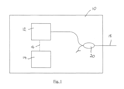
A first embodiment of the invention provides an optical network unit 10 as
shown
in Figure 1.
The optical network unit (ONU) 10 comprises a reflective semi-conductor
optical
amplifier (R-SOA) 12 and a driver 14 arranged to generate a drive signal 16 to
drive the R-
SOA 12.
The R-SOA 12 has a large optical confinement factor and is arranged to receive
a
portion of a downstream optical signal. In this example, the downstream
optical signal is
delivered to an optical input 18 of the ONU 10 and a portion of the downstream
optical
signal is routed to the R-SOA by an optical splitter 20. The downstream
optical signal has
a signal wavelength and a signal power.
The drive signal 16 is arranged to cause the R-SOA 12 to operate in saturation
at
the signal power. The driver 14 is arranged to generate the drive signal 16 to
cause the R-
SOA 12 to apply a return-to-zero (RZ) line code to the portion of the
downstream optical
signal received at the R-SOA 12 to form an upstream optical signal at the
signal
wavelength. The driver 14 is also arranged to generate the drive signal 16 to
cause the R-
SOA 12 to apply a phase modulation to the upstream optical signal.
An optical network unit 30 according to a second embodiment of the invention
is
shown in Figure 2.
The ONU 30 comprises an R-SOA 32 and a driver 34 arranged to generate a drive
signal 36. The R-SOA 32 has a large optical confinement factor, in this
example a
confinement factor of 4, and is arranged to receive a portion of a downstream
optical
signal. The downstream optical signal is received at an optical input 38 and a
portion of
the downstream optical signal is routed to the R-SOA 32 via an optical
splitter 40. The
downstream optical signal may comprise a continuous wave (CW) optical signal
or may
CA 02797726 2012-10-29
WO 2011/134536 PCT/EP2010/056456
8
comprise an inverse-return-to-zero (IRZ) line coded optical signal. The
downstream
optical signal has a signal wavelength and a signal power.
The driver 34 is arranged to generate a drive signal 36 to cause the R-SOA 32
to
operate in saturation at the signal power. The drive signal 36 is also
arranged to cause the
R-SOA 32 to apply an RZ line code to the portion of the downstream optical
signal to form
an upstream optical signal at the signal wavelength.
The driver is further arranged to generate a drive signal to drive the R-SOA
32 to
cause the R-SOA to apply a phase chirp to the logical "1" bits of the upstream
RZ optical
signal.
Due to gain-phase coupling in the R-SOA 32, a CW optical signal modulated by
the R-SOA 32 has a corresponding phase modulation applied to it, given by
0(t) - 2e ln(AG(t))
where - ae ff is the linewidth enhancement factor of the SOA.
As the gain of the R-SOA 32 is dependent upon the drive signal applied to the
R-
SOA, driving the R-SOA 32 with an RZ signal will result in two opposite phase
transitions
at each logical 1 bit, producing an upstream RZ line coded optical signal in
which each
logical 1 has a positive and a negative phase chirp applied to it, resulting
in a highly
chirped upstream optical signal. Since the amount of chirp is proportional to
the derivative
of the drive signal, driving with an RZ line code ensures that the upstream
optical signal is
continually phase chirped.
At low bit rates, such as the 1.25Gb/s bit rate typical of a passive optical
network,
the resulting chirp applied to the upstream optical signal introduces no
significant
chromatic dispersion penalty. An RZ line coded upstream optical signal is
thereby
produced which has a periodic phase variation, which effectively reduces the
coherence
time of the upstream optical signal. Applying a phase chirp to the upstream
optical signal
in this way significantly reduces the coherence time of the upstream optical
signal,
meaning that any reflections generated in an optical link, such as Rayleigh
back-scattering,
will interfere with the upstream optical signal incoherently, improving the
resilience of the
optical link to optical crosstalk.
CA 02797726 2012-10-29
WO 2011/134536 PCT/EP2010/056456
9
Figure 4 shows an RZ line coded upstream optical signal 60 and the
corresponding
phase modulation 62 applied to the RZ upstream optical signal.
An optical network unit 50 according to a third embodiment of the invention is
shown in Figure 3. The ONU 50 of this embodiment is substantially the same as
the ONU
of Figure 2, with the following modifications. The same reference numbers are
retained
for corresponding features.
In this embodiment, the downstream optical signal comprises an IRZ line coded
optical signal and the ONU 50 further comprises synchronisation apparatus 52.
The
synchronization apparatus 52 comprises an optical detector 54 and a clock and
data
recovery unit (CDR) 56.
A portion of the downstream optical signal is routed via the optical splitter
to the R-
SOA 32 and a further portion of the downstream optical signal is routed via
the optical
splitter 40 to the optical detector 54. The CDR 56 recovers the clock signal
from the
detected downstream optical signal and provides the clock signal 58 to the
driver 34.
The driver 34 is arranged to generate a drive signal to cause the R-SOA 32 to
apply
an RZ line code to the portion of the downstream optical signal to form an
upstream optical
signal which is interleaved by one half bit with respect to the IRZ downstream
optical
signal.
Figure 5 shows a passive optical network 70 according to a fourth embodiment
of
the invention. The passive optical network (PON) 70 comprises an optical line
terminal
(OLT) 72, an ONU 10 as shown in Figure 1, and an optical link 74.
The OLT 72 comprises an optical transmitter 76 arranged to generate a
downstream
optical signal having a signal wavelength and a signal power.
The optical link 74 is coupled between the OLT 72 and the ONU 10 and is
arranged
to transmit downstream and upstream optical signals between the OLT 72 and the
ONU
10.
A PON 80 according to a fifth embodiment of the invention is shown in Figure
6.
The PON 80 comprises an OLT 82, an ONU 50 as shown in Figure 3, and an optical
link
84.
The OLT 82 comprises an optical transmitter 86 and an optical receiver 88. The
optical transmitter 86 is arranged to generate an IRZ line coded downstream
optical signal
CA 02797726 2012-10-29
WO 2011/134536 PCT/EP2010/056456
which is coupled to the optical link 84 via an optical circulator 90. The
optical receiver 88
is arranged to receive an RZ line coded upstream optical signal and is coupled
to the
optical link 84 via the optical circulator 90.
The optical link 84 is coupled between the OLT 82 and the ONU 50 and is
arranged
5 to transmit downstream and upstream optical signals between the OLT 82 and
the ONU
50.
The construction and operation of the ONU 50 is as described in connection
with
Figure 3 above. It will be appreciated however that the ONU 30 of Figure 2 may
alternatively be used.
10 A PON 90 according to sixth embodiment of the invention is shown in Figure
7.
The PON 90 is substantially the same as the PON 80 of Figure 6, with the
following
modifications. The same reference numbers are retained for corresponding
features.
In this embodiment, the ONU 92 further comprises a bit error rate (BER) unit
94 to
analyse the received downstream optical signal and an optical delay line 96.
The driver 34
comprises a pulse pattern generator (PPG) 98 arranged to generate an RZ data
signal
comprising a pseudo random bit sequence (PRBS) having 8blOb line coding. The
driver
34 also comprises a 7 volt peak to peak electrical signal generator 100 which
generates the
drive signal for the R-SOA 32.
The optical link 84 is provided with a variable optical attenuator 102 and a
tunable
optical filter 104 having a 0.8 nm linewidth. The optical link 84 comprises 26
km of single
mode fibre (SMF).
In this embodiment the optical detector 88 in the OLT 94 is followed by a DC
signal block 106 and a low pass filter 108, and a BER unit 110 for analysis of
the detected
upstream optical signal.
The optical transmitter 86 comprises a pulse pattern generator (PPG) 112
arranged
to drive a DFB laser 114 with an IRZ line coded drive signal comprising a 1.25
Gb/s 8blOb
line coded PRBS. The resulting IRZ line coded downstream optical signal is
transmitted
via a polarisation scrambler (PS) 116 and a variable optical attenuator 118 to
the optical
circulator 90 for coupling into the optical link 84. The polarisation
scrambler 116 is
arranged to randomly rotate the signal polarization at a frequency of 6 kHz.
CA 02797726 2012-10-29
WO 2011/134536 PCT/EP2010/056456
11
A variable optical attenuator 120 is provided between the optical circulator
90 and
the optical detector 88.
The PON 90 of Figure 7 has been used to investigate the crosstalk mitigation
performance of the ONU 92, as follows.
At the OLT the DFB laser 114 was directly modulated by an IRZ sequence at 1.25
Gb/s, using an 8blOb line coded 2"-' PRBS, to emulate a GbE data stream. The
resulting
IRZ modulated optical signal was passed through the polarisation scrambler 116
which
randomly rotated the signal polarisation at a frequency of 6 kHz. The variable
optical
attenuators 102, 118 were used to set the signal-to-crosstalk ratio at the OLT
upstream
receiver 88. In this configuration the crosstalk contribution is provided
mainly by
Rayleigh back-scattered (RBS) light from the downstream optical signal. The
optical link
84 used here had an RBS return loss of approximately -34 dB. The variable
optical
attenuator 118 was used to set the RBS crosstalk power and the variable
optical attenuator
102 was used to set the upstream optical signal power.
At the ONU 92 the downstream optical signal was power split by the optical
splitter
40 and routed to the optical receiver 54 and the R-SOA 32. The ONU receiver
comprises
an avalanche photo detector (APD) 54 and a CDR unit 56. The recovered clock
signal was
used to assess the downstream optical signal performance and to provide
synchronization
for the upstream optical signal.
The upstream RZ signal was an inverted logic copy of the downstream IRZ
signal.
Figure 8 shows the optical penalty recorded at various crosstalk levels at the
upstream receiver 88. As can be seen, a 1 dB power penalty is recorded for a
signal to
crosstalk ratio of about 15dB. This is a significant result for a bi-
directional PON where a
significant outage should be expected at signal to crosstalk ratio levels of
about 25 dB.
The resilience of the PON 90 to synchronization errors between the downstream
and upstream optical signals was investigated and the measurement of the
penalty recorded
at the OLT receiver 88 for a synchronisation mismatch between the downstream
and
upstream signals is shown in Figure 9. As can be seen, 300 ps synchronisation
errors result
in less than 1 dB of optical power penalty at the OLT receiver.
A seventh embodiment of the invention provides a method 120 of transmitting
data
in a passive optical network. The steps of the method are shown in Figure 10.
CA 02797726 2012-10-29
WO 2011/134536 PCT/EP2010/056456
12
The method 120 comprises:
Receiving a portion of a downstream optical signal having a signal wavelength
at
an R-SOA having a large optical confinement factor 122; and
Driving the R-SOA to apply an RZ line code to the received portion of the
downstream optical signal to form an upstream optical signal at the signal
wavelength 124.
The R-SOA is driven to apply a phase modulation to the upstream optical signal
124.
The downstream optical signal may comprise a CW optical signal or an IRZ line
coded optical signal.
Figure 11 shows the steps of a method 130 of transmitting data in a passive
optical
network.
The method 130 comprises:
Receiving a portion of an IRZ line coded downstream optical signal having a
signal
wavelength at an R-SOA having a large optical confinement factor 132; and
Driving the R-SOA to apply an RZ line code to the portion of the downstream
optical signal to form an upstream optical signal at the signal wavelength
134. The method
further comprises driving the R-SOA to apply a phase chirp to light pulses of
the upstream
optical signal. The phase chirp is proportional to the derivative of the
optical power of a
respective light pulse of the upstream optical signal.