Language selection

Search

Patent 2797815 Summary

Third-party information liability

Some of the information on this Web page has been provided by external sources. The Government of Canada is not responsible for the accuracy, reliability or currency of the information supplied by external sources. Users wishing to rely upon this information should consult directly with the source of the information. Content provided by external sources is not subject to official languages, privacy and accessibility requirements.

Claims and Abstract availability

Any discrepancies in the text and image of the Claims and Abstract are due to differing posting times. Text of the Claims and Abstract are posted:

  • At the time the application is open to public inspection;
  • At the time of issue of the patent (grant).
(12) Patent: (11) CA 2797815
(54) English Title: SUPER CAPACITOR
(54) French Title: SUPER CONDENSATEUR
Status: Granted
Bibliographic Data
(51) International Patent Classification (IPC):
  • H05F 7/00 (2006.01)
  • H01G 4/005 (2006.01)
  • H01G 4/08 (2006.01)
  • H01G 4/38 (2006.01)
  • H02J 15/00 (2006.01)
(72) Inventors :
  • MELITO, CARL FRANK (United States of America)
(73) Owners :
  • MELITO INC (United States of America)
(71) Applicants :
  • MELITO INC (United States of America)
(74) Agent: OSLER, HOSKIN & HARCOURT LLP
(74) Associate agent:
(45) Issued: 2015-10-13
(86) PCT Filing Date: 2010-12-29
(87) Open to Public Inspection: 2011-11-10
Examination requested: 2012-10-29
Availability of licence: N/A
(25) Language of filing: English

Patent Cooperation Treaty (PCT): Yes
(86) PCT Filing Number: PCT/US2010/062389
(87) International Publication Number: WO2011/139315
(85) National Entry: 2012-10-29

(30) Application Priority Data:
Application No. Country/Territory Date
12/772,213 United States of America 2010-05-02

Abstracts

English Abstract

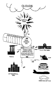
A super conducting super capacitor and method forming massive embedded capacitors connected in parallel over a very wide radius that can vary from a few square feet to hundreds or thousands of square miles, and more, is disclosed. The super conducting super capacitor is formed within a water proof vacuum housing to keep out water and humidity by depositing a plurality of alternating layers of dielectric material between each layer of conducting material, whereby one or more electrodes are situated on each dielectric layer, thus forming a super conducting super capacitor having at least one probe electrode exuding from said housing, and connected to the one or more electrodes, for receiving electric charge from a lightning source for example. One can contemplate many dielectric layers separating many conductor layers from a few layers to thousands, and possibly even millions or more layers delineated, for example, to define a multilayer capacitive structure capable of providing electric power to supplement or replace other sources of electric power that harm the environment.


French Abstract

La présente invention concerne un supercondensateur supraconducteur et un procédé de formation de condensateurs intégrés massifs reliés en parallèle sur un rayon très large qui peut varier de quelques pieds carrés à des centaines ou des milliers de miles carrés et plus. Le supercondensateur supraconducteur est formé dans un logement sous vide étanche pour éloigner l'eau et l'humidité par dépôt de plusieurs couches alternées de matériau diélectrique entre chaque couche de matériau conducteur, une ou plusieurs électrodes étant situées sur chaque couche diélectrique, formant ainsi un supercondensateur supraconducteur ayant au moins une électrode de sonde faisant saillie dudit logement et relié à la ou aux électrodes, pour recevoir une charge électrique d'une source de foudroiement, par exemple. On peut prévoir de nombreuses couches diélectriques séparant de nombreuses couches conductrices de quelques couches délinées, voire de milliers de couches délinées, et éventuellement de millions de couches délinées ou plus, par exemple, afin de définir une structure capacitive multicouche capable de fournir une énergie électrique afin de compléter ou de remplacer d'autres sources d'énergie électrique qui nuisent à l'environnement.

Claims

Note: Claims are shown in the official language in which they were submitted.


The embodiments of the present invention for which an exclusive property or
privilege is claimed are defined as follows:
1. A super capacitor comprising:
a plurality of embedded parallel capacitors having radii in excess of ten feet

enclosed in a water proof housing;
at least one metallic probe connected to said capacitors and exuding from said

housing for receiving electrical energy from a lightning source to charge said
super
capacitors.
2. The super capacitor of claim 1, wherein a massive battery is
electrically
connected to said super capacitor.
3. The super capacitor of claim 1, wherein said super capacitor is
electrically
connected to an electrical power grid.
4. The super capacitor of claim 2, wherein said massive battery is
electrically
connected to an electrical power grid.
5. The super capacitor of any one of claims 1 to 4, wherein said embedded
parallel capacitors have sand as a dielectric material.
6. The super capacitor of any one of claims 1 to 4, wherein said embedded
parallel capacitors have iron as a conductor material.
8

7. The super capacitor of any one of claims 1 to 4, wherein said embedded
parallel capacitors have silicon as a dielectric material.
8. The super capacitor of any one of claims 1 to 4, wherein said embedded
parallel capacitors have metallic sheets for conductor material.
9. A method of capturing electrical energy from lightning, comprising the
steps
of:
placing near a lightning source at least one probe electrode of a super
capacitor having alternating layers of conductors and dielectric material each
having
radii in excess of ten feet to form a multilayer parallel capacitive
structure, said
multilayer parallel capacitive structure being formed of embedded massive
parallel
capacitors within a water proof housing;
receiving electrical energy from a lightning strike using said at least one
probe
electrode connected to said embedded massive parallel capacitors, said at
least one
probe electrode exuding from said housing.
10. The method of claim 9, wherein said conductors comprise metallic sheets
and
said dielectric material is silicon.
11. The method of claim 9, comprising the additional step of electrically
connecting a massive battery to said super capacitor.
9

12. The method of claim 9, comprising the additional step of electrically
connecting said super capacitor to an electrical power grid to function as an
alternative
energy source.
13. A method of generating electricity, comprising the steps of:
generating lightning by ionizing the atmosphere near at least one probe
electrode of a super capacitor, said super capacitor having alternating layers
of
conductors and dielectric material each having any shape with radii at a
shortest side
in excess of ten feet to form a multilayer parallel capacitive structure, said
multilayer
parallel capacitive structure being formed of at least one embedded massive
parallel
capacitor within a water proof housing; and
receiving electrical energy from a lightning strike through said at least one
probe electrode connected to said at least one embedded massive parallel
capacitor,
said at least one probe electrode exuding from said water proof housing.
14. The method of generating electricity according to claim 13, wherein
ionizing
the atmosphere comprises cloud seeding.

Description

Note: Descriptions are shown in the official language in which they were submitted.


CA 02797815 2014-11-10
SUPER CAPACITOR
FIELD OF THE INVENTION
This invention relates generally to massive electrical circuits and their
fabrication,
housed within a massive water resistant vacuum nonconductive shell made of
concrete,
ceramic, or other like nonconductive material, using layers of localized
abundant natural
resources such as sand, or other dielectric materials, etc., as insulators
(whether human
fabricated or naturally occurring); human fabricated or naturally occurring
layers of metallic
materials such as iron, aluminum, etc., as conductors; a metallic probe
emanating from the
housing and connected in parallel with each conductive layer; and human
generated or
naturally occurring phenomena such as lightning, as a source of power to the
probe. More
particularly, this invention relates to a process for forming a
macroelectronic assembly with
integral multilayer capacitors that have a wide range of capacitance values
based on their
very wide radii and number of layers formed in its housing. Electricity thusly
captured can
then be stored and distributed for human consumption. A new type of electrical
power plant
is contemplated employing this super capacitor technology, providing
electrical energy to the
power grid and for use by electrical filling stations for electrical transport
vehicles, such as
cars, trucks, buses, ships, trains and aircraft.
BACKGROUND
Microelectronic capacitors are typically formed by patterning a conductive
region on
a ceramic substrate to define a bottom electrode, depositing a thin layer of a
dielectric
material over the bottom electrode to form the dielectric for the
microelectronic capacitor,
1

CA 02797815 2014-11-10
and then forming a second electrode over the dielectric, patterned to form the
microelectronic
capacitor, using a second conductive region above the dielectric material. In
this way,
microelectronic capacitors store electric charge, and since work must be done
to charge the
microelectronic capacitor, the microelectronic capacitor will also store
electric potential
energy. If one considers an example isolated metallic sphere of radius R, any
electric charge
stored on this sphere, call it Q, can be articulated as a potential:
V = 1 Q
47cce R
such that the amount of charge stored on the sphere is directly proportional
to the potential
(V). This proportionality exists for any conductor of any shape or size.
Capacitance (C) of
this single conductor is large if the conductor is capable of storing a large
amount of charge at
a low potential, so that the relation:
Q = CV becomes C = Q., = 0 = 47reoR
V 1 S1
4neo R
Therefore, the capacitance of the sphere increases with its radius, and many
such spheres
wired together in parallel creates a net capacitance that is the sum of their
individual
capacitances. Furthermore, capacitors store not only electric charge (Q), but
also electric
potential energy (U), which can be expressed roughly as:
U = 1/2 02,
C
2

CA 02797815 2014-11-10
(ignoring the energy density in the dielectric layers). The electric potential
energy (U) is also
the total amount of work that must be performed to charge the capacitor.
What is needed is a macroelectronic circuit referred to herein as a super
capacitor and
method that exploits the above relationships to be used to capture and store
the electric
charge of lightning, whether naturally occurring or human generated, as an
alternative energy
source for human consumption. After determination of the total energy range
generated by
lightning strikes in a particular setting, an optimum radius and number of
embedded parallel
layers of capacitors forming the super capacitor of the present invention can
be established
based on the area of land, or other substrate, that is available to support
the super capacitor
housing of the present invention.
SUMMARY
A super capacitor and method forming massive embedded capacitors connected in
parallel over a very wide radius that can vary from a few square feet to
hundreds or thousands
of square miles, and more, is disclosed. The super capacitor is formed within
a water proof
vacuum housing to keep out water and humidity by depositing a plurality of
alternating layers
of dielectric material between each layer of conducting material, whereby one
or more
electrodes are situated on each dielectric layer, thus forming a super
capacitor having at least
one probe electrode exuding from said housing, and connected to the one or
more electrodes,
for receiving electric charge from a lightning source for example. One can
contemplate many
dielectric layers separating many conductor layers from a few layers to
thousands, and
possibly even millions or more layers delineated, for example, to define a
multilayer
capacitive structure capable of providing electric power to supplement or
replace other
sources of electric power that harm the environment.
3

CA 02797815 2014-11-10
In one aspect of the present invention there is provided a super capacitor
comprising:
a plurality of embedded parallel capacitors having radii in excess of ten feet
enclosed in a
water proof housing; at least one metallic probe connected to said capacitors
and exuding
from said housing for receiving electrical energy from a lightning source to
charge said super
capacitors.
In another aspect of the present invention there is provided a method of
capturing
electrical energy from lightning, comprising the steps of: placing near a
lightning source at
least one probe electrode of a super conducting super capacitor having
alternating layers of
conductors and dielectric material each having radii in excess of ten feet to
form a multilayer
parallel capacitive structure, said multilayer parallel capacitive structure
being formed of
embedded massive parallel capacitors within a water proof housing; receiving
electrical
energy from a lightning strike using said at least one probe electrode
connected to said
embedded massive parallel capacitors, said at least one probe electrode
exuding from said
housing.
In a further aspect of the present invention there is provided a method of
generating
electricity, comprising the steps of: generating lightning by ionizing the
atmosphere near at
least one probe electrode of a super capacitor, said super capacitor having
alternating layers
of conductors and dielectric material each having any shape with radii at a
shortest side in
excess of ten feet to form a multilayer parallel capacitive structure, said
multilayer parallel
capacitive structure being formed of at least one embedded massive parallel
capacitor within
a water proof housing; and receiving electrical energy from a lightning strike
through said at
least one probe electrode connected to said at least one embedded massive
parallel capacitor,
said at least one probe electrode exuding from said water proof housing.
4

CA 02797815 2014-11-10
BRIEF DESCRIPTION OF THE DRAWINGS
FIG. 1 illustrates one contemplated embodiment of a super capacitor by which
massive embedded super capacitors are connected in parallel over a very large
land area in
accordance with certain embodiments of the present invention using a ceramic
material for a
water proof housing, silicon as the dielectric insulator material forming each
insulating layer,
and metallic sheets as conductors forming each conducting layer.
FIG. 2 is a block diagram that illustrates a naturally occurring embodiment of
the
method of the present invention.
FIG. 3 is a block diagram that illustrates a human controlled embodiment of
the
method of the present invention.
DETAILED DESCRIPTION
Detailed embodiments of the present invention are disclosed herein; however,
it is to
be understood that the disclosed embodiments are merely exemplary of the
invention, which
can be embodied in various forms. Therefore, specific structural and
functional details
disclosed herein are not to be interpreted as limiting, but merely as a basis
for the claims and
as a representative basis for teaching one skilled in the art to variously
employ the present
invention in virtually any appropriately detailed structure. Further, the
terms and phrases used
herein are not intended to be limiting; but rather, to provide an
understandable description of
the invention.
The terms a or an, as used herein, are defined as one or more than one. The
term
plurality, as used herein, is defined as two or more than two. The term
another, as used
herein, is defined as at least a second or more. The terms including and/or
having, as used
herein, are defined as comprising (i.e., open language). While a particular
configuration for

CA 02797815 2014-11-10
the invention is shown in FIG. 1, those skilled in the art will appreciate
that variations and
modifications are possible, and such variations and modifications are within
the scope of this
invention.
Referring now to FIG. 1, the macroelectronic circuit of the present invention,
referred
to herein as the super capacitor 100 (hereinafter SC), is shown as having
alternating layers of
conductors 20 and dielectric material 30, similar in structure to prior art
microelectronic
parallel capacitor circuits, and at least one probe electrode 10 for receiving
the lightning
strike. The primary differences over prior art capacitors are size, power
scale, purpose, and
lightning as a power source. One embodiment of the present invention
contemplates
connecting the SC 100 to a massive battery system 200 (hereinafter massive
battery) that
receives the generated electrical energy so as to free up the SC 100 for more
lightning strikes.
The massive battery 200 can also be linked with an electrical power grid 300
that can
comprise direct connections to Electric Train Stations, Factories, and
Electric Filling Stations
for transfer to transport vehicles such as electric trucks, cars, ships and
aircraft.
Referring now to FIG. 2, the best mode for practicing the invention is to
utilize free
and naturally occurring lightning. However, this method limits the invention
to use in
geographic areas where there is substantial rain, and thus naturally occurring
lightning.
Referring now to FIG 3, an alternative, but more costly, method to practice
the
invention, but which overcomes geographic limitations, is to create lightning
by ionization of
the atmosphere, such as by silver iodide cloud seeding to generate rain, and
therefore,
lightning.
While the invention has been described in conjunction with specific
embodiments, it
is evident that many alternatives, modifications, permutations and variations
will become
apparent to those of ordinary skill in the art in light of the foregoing
description. Accordingly,
6

CA 02797815 2014-11-10
it is intended that the present invention embrace all such alternatives,
modifications and
variations as fall within the scope of the appended claims.
7

Representative Drawing
A single figure which represents the drawing illustrating the invention.
Administrative Status

For a clearer understanding of the status of the application/patent presented on this page, the site Disclaimer , as well as the definitions for Patent , Administrative Status , Maintenance Fee  and Payment History  should be consulted.

Administrative Status

Title Date
Forecasted Issue Date 2015-10-13
(86) PCT Filing Date 2010-12-29
(87) PCT Publication Date 2011-11-10
(85) National Entry 2012-10-29
Examination Requested 2012-10-29
(45) Issued 2015-10-13

Abandonment History

There is no abandonment history.

Maintenance Fee

Last Payment of $263.14 was received on 2023-12-19


 Upcoming maintenance fee amounts

Description Date Amount
Next Payment if standard fee 2024-12-30 $347.00
Next Payment if small entity fee 2024-12-30 $125.00

Note : If the full payment has not been received on or before the date indicated, a further fee may be required which may be one of the following

  • the reinstatement fee;
  • the late payment fee; or
  • additional fee to reverse deemed expiry.

Patent fees are adjusted on the 1st of January every year. The amounts above are the current amounts if received by December 31 of the current year.
Please refer to the CIPO Patent Fees web page to see all current fee amounts.

Payment History

Fee Type Anniversary Year Due Date Amount Paid Paid Date
Request for Examination $800.00 2012-10-29
Application Fee $400.00 2012-10-29
Maintenance Fee - Application - New Act 2 2012-12-31 $100.00 2012-10-29
Maintenance Fee - Application - New Act 3 2013-12-30 $100.00 2013-11-04
Maintenance Fee - Application - New Act 4 2014-12-29 $100.00 2014-11-24
Final Fee $300.00 2015-06-19
Maintenance Fee - Patent - New Act 5 2015-12-29 $200.00 2015-12-29
Maintenance Fee - Patent - New Act 6 2016-12-29 $200.00 2016-12-28
Maintenance Fee - Patent - New Act 7 2017-12-29 $200.00 2017-10-17
Maintenance Fee - Patent - New Act 8 2018-12-31 $400.00 2019-12-18
Maintenance Fee - Patent - New Act 9 2019-12-30 $200.00 2019-12-18
Maintenance Fee - Patent - New Act 10 2020-12-29 $250.00 2020-12-03
Maintenance Fee - Patent - New Act 11 2021-12-29 $255.00 2021-12-17
Maintenance Fee - Patent - New Act 12 2022-12-29 $254.49 2022-12-29
Maintenance Fee - Patent - New Act 13 2023-12-29 $263.14 2023-12-19
Owners on Record

Note: Records showing the ownership history in alphabetical order.

Current Owners on Record
MELITO INC
Past Owners on Record
None
Past Owners that do not appear in the "Owners on Record" listing will appear in other documentation within the application.
Documents

To view selected files, please enter reCAPTCHA code :


To view images, click a link in the Document Description column. To download the documents, select one or more checkboxes in the first column and then click the "Download Selected in PDF format (Zip Archive)" or the "Download Selected as Single PDF" button.

List of published and non-published patent-specific documents on the CPD .

If you have any difficulty accessing content, you can call the Client Service Centre at 1-866-997-1936 or send them an e-mail at CIPO Client Service Centre.


Document
Description 
Date
(yyyy-mm-dd) 
Number of pages   Size of Image (KB) 
Maintenance Fee Payment 2019-12-18 1 33
Maintenance Fee Payment 2020-12-03 1 33
Maintenance Fee Payment 2021-12-17 1 33
Maintenance Fee Payment 2022-12-29 1 33
Claims 2012-10-30 3 114
Drawings 2013-03-22 3 42
Description 2013-03-22 6 198
Abstract 2012-10-29 2 81
Claims 2012-10-29 3 97
Drawings 2012-10-29 3 48
Description 2012-10-29 6 200
Representative Drawing 2012-12-19 1 15
Cover Page 2013-01-03 1 52
Description 2014-11-10 7 232
Claims 2014-11-10 3 72
Drawings 2014-11-10 3 41
Representative Drawing 2015-09-23 1 10
Cover Page 2015-09-23 2 53
Maintenance Fee Payment 2023-12-19 1 33
Fees 2014-11-24 1 44
PCT 2012-10-29 13 490
Assignment 2012-10-29 3 110
Prosecution-Amendment 2012-10-29 3 87
Prosecution-Amendment 2013-03-22 5 123
Prosecution-Amendment 2013-04-12 1 27
Prosecution-Amendment 2014-05-08 2 55
Fees 2013-11-04 1 43
Prosecution-Amendment 2014-11-10 22 737
Final Fee 2015-06-19 2 63
Maintenance Fee Payment 2015-12-29 2 110
Maintenance Fee Payment 2016-12-28 1 43