Note: Descriptions are shown in the official language in which they were submitted.
CA 02797826 2016-04-15
ELECTROCHROMIC DEVICES
TECHNICAL FIELD OF THE INVENTION
[0001] This disclosure relates to electrochromic devices, methods of
fabrication,
associated apparatus and the like.
BACKGROUND
[0002] Electrochromism is a phenomenon in which a material exhibits a
reversible
electrochemically-mediated change in an optical property when placed in a
different
electronic state, typically by being subjected to a voltage change. The
optical property is
typically one or more of color, transmittance, absorbance, and reflectance.
One well known
electrochromic material, for example, is tungsten oxide (W03). Tungsten oxide
is a cathodic
electrochromic material in which a coloration transition, transparent to blue,
occurs by
electrochemical reduction.
100031 Electrochromic materials may be incorporated into, for example, windows
and
mirrors. The color, transmittance, absorbance, and/or reflectance of such
windows and
mirrors may be changed by inducing a change in the electrochromic material.
One well
known application of electrochromic materials, for example, is the rear view
mirror in some
cars. In these electrochromic rear view mirrors, the reflectivity of the
mirror changes at night
so that the headlights of other vehicles are not distracting to the driver.
[0004] While electrochromism was discovered in the 1960's, electrochromic
devices still
unfortunately suffer various problems and have not begun to realize their full
commercial
potential. Advancements in electrochromic technology, apparatus and related
methods of
making and/or using them, are needed.
SUMMARY OF INVENTION
[0005] A typical electrochromic device includes an electrochromic ("EC")
electrode layer
and a counter electrode ("CE") layer, separated by an ionically conductive
("IC") layer that is
highly conductive to ions and highly resistive to electrons. In other words,
the ionically
conductive layer permits transport of ions but blocks electronic current. As
conventionally
understood, the ionically conductive layer therefore prevents shorting between
the
1
CA 02797826 2012-10-29
WO 2011/137080 PCT/US2011/033822
electrochromic layer and the counter electrode layer. The ionically conductive
layer allows
the electrochromic and counter electrodes to hold a charge and thereby
maintain their
bleached or colored states. In conventional electrochromic devices, the
components form a
stack with the ion conducting layer sandwiched between the electrochromic
electrode and the
counter electrode. The boundaries between these three stack components are
defined by
abrupt changes in composition and/or microstructure. Thus, the devices have
three distinct
layers with two abrupt interfaces.
[0006] Quite surprisingly, the inventors have discovered that high quality
electrochromic
devices can be fabricated without depositing an ionically-conducting
electronically-insulating
layer. In accordance with certain embodiments, the counter electrode and
electrochromic
electrodes are formed immediately adjacent one another, often in direct
contact, without
separately depositing an ionically-conducting layer. It is believed that
various fabrication
processes and/or physical or chemical mechanisms produce an interfacial region
between
contacting electrochromic and counter electrode layers, and this interfacial
region serves at
least some functions of an ionically conductive electronically-insulating
layer in conventional
devices. Certain mechanisms that may be key to forming the interfacial region
are described
below.
[0007] The interfacial region typically, though not necessarily, has a
heterogeneous
structure that includes at least two discrete components represented by
different phases and/or
compositions. Further, the interfacial region may include a gradient in these
two or more
discrete components. The gradient may provide, for example, a variable
composition,
microstructure, resistivity, dopant concentration (for example, oxygen
concentration), and/or
stoichiometry.
[0008] In addition to the above discoveries, the inventors have observed that
in order to
improve device reliability, two layers of an electrochromic device, the
electrochromic (EC)
layer and the counter electrode (CE) layer, can each be fabricated to include
defined amounts
of lithium. Additionally, careful choice of materials and morphology and/or
microstructure
of some components of the electrochromic device provides improvements in
performance
and reliability. In some embodiments, all layers of the device are entirely
solid and
inorganic.
[0009] Consistent with above observations and discoveries, the inventors have
discovered
that formation of the EC-IC-CE stack need not be done in the conventional
sequence,
EC¨IC¨CE or CE¨IC¨EC, but rather an ion conducting electronically-insulating
region,
serving as an IC layer, can be formed after formation of the electrochromic
layer and the
2
CA 02797826 2012-10-29
WO 2011/137080 PCT/US2011/033822
counter electrode layer. That is, the EC-CE (or CE-EC) stack is formed first,
then an
interfacial region serving some purposes of an IC layer is formed between the
EC and CE
layers using components of one or both of the EC and CE layers at the
interface of the layers.
Methods of the invention not only reduce fabrication complexity and expense by
eliminating
one or more process steps, but provide devices showing improved performance
characteristics.
[0010] Thus, one aspect of the invention is a method of fabricating an
electrochromic
device, the method including: forming an electrochromic layer including an
electrochromic
material; forming a counter electrode layer in contact with the electrochromic
layer without
first providing an ion conducting electronically-insulating layer between the
electrochromic
layer and the counter electrode layer; and forming an interfacial region
between the
electrochromic layer and the counter electrode layer, where the interfacial
region is
substantially ion conducting and substantially electronically-insulating. The
electrochromic
layer and counter electrode layer are typically, but not necessarily, made of
one or more
materials that are more electronically conductive than the interfacial region
but may have
some electronically resistive character. The interfacial region can contain
component
materials of the EC layer and/or the CE layer, and in some embodiments, the EC
and CE
layers contain component materials of the interfacial region. In one
embodiment, the
electrochromic layer includes W03. In some embodiments, the EC layer includes
W03, the
CE layer includes nickel tungsten oxide (NiWO), and the IC layer includes
lithium tungstate
(Li2W04).
[0011] Heating may be applied during deposition of at least a portion of the
electrochromic
layer. In one embodiment, where the EC layer includes W03, heating is applied
after each of
a series of depositions via sputtering in order to form an EC layer with a
substantially
polycrystalline microstructure. In one embodiment, the electrochromic layer is
between
about 300 nm and about 600 nm thick, but the thickness may vary depending upon
the
desired outcome which contemplates formation of the interfacial region after
deposition of
the EC-CE stack. In some embodiments, the W03 is substantially
polycrystalline. In some
embodiments, an oxygen rich layer of W03 can be used as a precursor to the
interfacial
region. In other embodiments the W03 layer is a graded layer with varying
concentrations of
oxygen in the layer. In some embodiments, lithium is a preferred ion species
for driving the
electrochromic transitions, and stack or layer lithiation protocols are
described. Specifics of
the formation parameters and layer characteristics are described in more
detail below.
3
CA 02797826 2012-10-29
WO 2011/137080 PCT/US2011/033822
[0012] Another aspect of the invention is a method of fabricating an
electrochromic device,
the method including: (a) forming either an electrochromic layer including an
electrochromic
material or a counter electrode layer including a counter electrode material;
(b) forming an
intermediate layer over the electrochromic layer or the counter electrode
layer, where the
intermediate layer includes an oxygen rich form of at least one of the
electrochromic
material, the counter electrode material and an additional material, where the
additional
material includes distinct electrochromic and/or counter electrode material,
the intermediate
layer not substantially electronically-insulating; (c) forming the other of
the electrochromic
layer and the counter electrode layer; and (d) allowing at least a portion of
the intermediate
layer to become substantially electronically-insulating and substantially ion
conducting.
Specifics of the formation parameters and layer characteristics for this
method are also
described in more detail below.
[0013] In other embodiments, a substantially electronically-insulating and ion
conducting
region is formed on, and after formation of, the electrochromic or the counter
electrode layer,
as a result of heating a superstoichiometric oxygen form of the electrochromic
or the counter
electrode layer in the presence of lithium. The other of the electrochromic or
the counter
electrode layer is formed after, and on, the substantially electronically-
insulating and ion
conducting region thus formed. In one example, the electrochromic layer is
formed first, for
example on a glass substrate having a transparent conductive oxide thereon.
The
electrochromic layer can have a first sub-layer of a metal oxide that is
stoichiometric or sub-
stoichiometric in oxygen and a top layer that is superstoichiometric in
oxygen, or the
electrochromic layer can be a graded composition with at least a
superstoichiometric upper
portion. Superstoichiometric metal oxides are exposed to lithium and heated to
form the
substantially electronically-insulating and ion conducting region. The counter
electrode is
formed thereon as part of fabrication of a functioning electrochromic stack.
Further details of
these methods are described below.
[0014] In other embodiments, a substantially electronically-insulating and ion
conducting
interfacial region is formed after formation of the electrochromic or the
counter electrode
layer, as a result of exposing a superstoichiometric oxygen form of the
electrochromic or the
counter electrode layer to lithium, followed by formation of the other of the
electrochromic or
the counter electrode layer. That is, during formation of the second
electrode, a lithium flux
is driven from the first formed electrode layer (having been exposed to
lithium) into the
second formed, or forming, electrode layer. It is believed that this lithium
flux may drive
formation of the substantially electronically-insulating and ion conducting
interfacial region.
4
CA 02797826 2012-10-29
WO 2011/137080 PCT/US2011/033822
In one example, the electrochromic layer is formed first, for example on a
glass substrate
having a transparent conductive oxide thereon. The electrochromic layer can
have a first sub-
layer of a metal oxide that is stoichiometric or sub-stoichiometric in oxygen
and a top layer
that is superstoichiometric in oxygen, or the electrochromic layer can be a
graded
composition with at least a superstoichiometric upper portion.
Superstoichiometric metal
oxides are exposed to lithium, for example sputtering lithium. The counter
electrode is
formed thereon where the aforementioned lithium flux forms the substantially
electronically-
insulating and ion conducting interfacial region between the electrochromic
and
counterelectrode layers. Further details of these methods are described below.
[0015] Another aspect of the invention is an apparatus for fabricating an
electrochromic
device, including: an integrated deposition system including: (i) a first
deposition station
containing a material source configured to deposit an electrochromic layer
including an
electrochromic material; and (ii) a second deposition station configured to
deposit a counter
electrode layer including a counter electrode material; and a controller
containing program
instructions for passing the substrate through the first and second deposition
stations in a
manner that sequentially deposits a stack on the substrate, the stack having
an intermediate
layer sandwiched in between the electrochromic layer and the counter electrode
layer; where
either or both of the first deposition station and the second deposition
station are also
configured to deposit the intermediate layer over the electrochromic layer or
the counter
electrode layer, and where the intermediate layer includes an oxygen rich form
of the
electrochromic material or the counter electrode material and where the first
and second
deposition stations are interconnected in series and operable to pass a
substrate from one
station to the next without exposing the substrate to an external environment.
In one
embodiment, apparatus of the invention are operable to pass the substrate from
one station to
the next without breaking vacuum and may include one or more lithiation
stations operable to
deposit lithium from a lithium-containing material source on one or more
layers of the
electrochromic device. In one embodiment, apparatus of the invention are
operable to
deposit the electrochromic stack on an architectural glass substrate.
Apparatus of the
invention need not have a separate target for fabrication of an ion conducting
layer.
[0016] Another aspect of the invention is an electrochromic device including:
(a) an
electrochromic layer including an electrochromic material; (b) a counter
electrode layer
including a counter electrode material; and (c) an interfacial region between
the
electrochromic layer and the counter electrode layer, where the interfacial
region includes an
electronically-insulating ion conducting material and at least one of the
electrochromic
5
CA 02797826 2016-04-15
material, the counter electrode material and an additional material, where the
additional
material includes distinct electrochromic and/or counter electrode material.
In some
embodiments the additional material is not included; in these embodiments the
interfacial
region includes at least one of the electrochromic material and the counter
electrode material.
Variations in the composition and morphology and/or microstructure of the
interfacial region
are described in more detail herein. Electrochromic devices described herein
can be
incorporated into windows, in one embodiment, architectural glass scale
windows.
According to another aspect of the present invention, there is provided a
method of
fabricating an electrochromic device, the method comprising the following
steps:
(a) forming either an electrochromic layer including an electrochromic
material or a
counter electrode layer including a counter electrode material;
(b) forming an intermediate layer over the electrochromic layer or the counter
electrode
layer, where the intermediate layer includes an oxygen rich form of at least
one of
the electrochromic material, the counter electrode material and an additional
material, where the additional material includes distinct electrochromic or
counter
electrode material;
(c) exposing the intermediate layer to lithium; and
(d) heating the stack formed thereby converting at least part of the
intemiediate layer to
a region, coextensive with an area of the intermediate layer, comprising an
electronically-insulating ionically-conducting material and the material of
the
intermediate layer.
According to another aspect of the present invention, there is provided a
method of
fabricating an electrochromic device, the method comprising the following
steps:
(a) forming a stack comprising either an electrochromic layer including an
electrochromic material or a counter electrode layer including a counter
electrode
material, wherein the electrochromic layer or the counter electrode layer
formed
comprises a superstoichiometric oxygen portion in an upper region of, and
coextensive with, an area of the electrochromic or counter electrode layer;
(b) exposing the superstoichiometric oxygen portion to lithium; and
(c) heating to convert at least part of the superstoichiometric oxygen portion
to a region,
coextensive with an area of the superstoichiometric oxygen portion, comprising
an
6
CA 02797826 2016-04-15
electronically-insulating ionically-conducting material and the material of
the
superstoichiometric oxygen portion.
According to another aspect of the present invention, there is provided a
method of
fabricating an electrochromic device, the method comprising the steps of:
(a) forming either an electrochromic layer including an electrochromic
material or a
counter electrode layer including a counter electrode material;
(b) forming an intermediate layer over the electrochromic layer or the counter
electrode
layer, where the intermediate layer includes an oxygen rich form of at least
one of
the electrochromic material, the counter electrode material and an additional
material, where the additional material includes distinct electrochromic or
counter
electrode material,
(c) exposing the intermediate layer to lithium; and
(d) depositing the other of the electrochromic layer and the counter electrode
layer on
the intermediate layer thereby converting at least part of the intermediate
layer to a
region, coextensive with an area of the intermediate layer, comprising an
electronically-insulating ionically-conducting material and the material of
the
intermediate layer.
According to another aspect of the present invention, there is provided a
method of
fabricating an electrochromic device, the method comprising the following
steps:
(a) forming a stack comprising either an electrochromic layer including an
electrochromic material or a counter electrode layer including a counter
electrode
material, wherein the electrochromic layer or the counter electrode layer
formed
comprises a superstoichiometric oxygen portion in an upper region of, and
coextensive with, an area of the electrochromic or counter electrode layer;
(b) exposing the superstoichiometric oxygen portion to lithium; and
(c) depositing the other of the electrochromic layer and the counter electrode
layer on
the superstoichiometric oxygen portion thereby converting at least part of the
superstoichiometric oxygen portion to a region, coextensive with an area of
the
superstoichiometric oxygen portion, comprising an electronically-insulating
ionically-conducting material and the material of the superstoichiometric
oxygen
portion.
6a
According to another aspect of the present invention, there is provided a
method of
fabricating an electrochromic device, the method comprising:
((ba)) ffoormrmiinngg
annoeolunecttrerocehrl000tmroiedelalyneyrercoinmpoorinstianogt
anwitenletchteroecihr000trmooichrmomatejo layer
er without
first providing an ion conducting electronically insulating layer between the
electrochromic layer and the counter electrode layer, wherein the counter
electrode
layer comprises a counter electrode material; and
(c) forming an interfacial region between the electrochromic layer and the
counter
electrode layer, formed using components of one or both the electrochromic
layer
and counter electrode layer, wherein said interfacial region is substantially
ion
conducting and substantially electronically insulating.
According to another aspect of the present invention, there is provided an
electrochromic device comprising:
(a) an electrochromic layer comprising an electrochromic material;
(b) a counter electrode layer comprising a counter electrode material; and
(c) an interfacial region between the electrochromic layer and the counter
electrode
layer, wherein the interfacial region comprises a mixture of: (i) a
substantially
electronically insulating ion conductor material, and (ii) the electrochromic
material,
1
the counter electrode material and/or an additional material, where the
additional
material includes distinct electrochromic or counter electrode material,
wherein the
electrochromic material is operable for a first electrochromic transition,
wherein the
counter electrode material is operable for a second electrochromic transition,
and
wherein the electrochromic device has only one electrochromic layer and only
one
counter electrode layer.
According to another aspect of the present invention, there is provided an
electrochromic device comprising:
(a) an electrochromic layer comprising tungsten oxide;
(b) a counter electrode layer comprising nickel tungsten oxide; and
(c) an interfacial region between the electrochromic layer and the counter
electrode
layer, wherein the interfacial region comprises a mixture of lithium tungstate
and at
least one of tungsten oxide and nickel tungsten oxide.
6b
CA 2797826 2017-07-12
According to another aspect of the present invention, there is provided an
electrochromic device comprising:
(a) an electrochromic layer comprising an electrochromic metal oxide operable
for
undergoing a first electrochromic transition;
(b) a counter electrode layer comprising a counter electrode material operable
for
undergoing a second electrochromic transition; and
(c) an intermediate layer between the electrochromic layer and the counter
electrode
layer, wherein the intermediate layer comprises (i) an oxygen rich form of the
electrochromic metal oxide in the electrochromic layer and/or (ii) an oxygen
rich
form of the counter electrode material in the counter electrode layer.
According to another aspect of the present invention, there is provided an
apparatus
for fabricating an electrochromic device, comprising:
(a) an integrated deposition system comprising:
(i) a first deposition station containing a first target comprising a first
material for
depositing a layer of an electrochromic material on a substrate when the
substrate is positioned in the first deposition station, and
(ii) a second deposition station containing a second target comprising a
second
material for depositing a layer of a counter electrode material on the
substrate
when the substrate is positioned in the second deposition station; and
(b) a controller containing program instructions provided on a non-transitory
medium
for passing the substrate through the first and second deposition stations in
a manner
that sequentially deposits a stack on the substrate, the stack comprising the
layer of
electrochromic material in direct contact with the layer of counter electrode
material,
without an ion conducting layer between the layer of electrochromic material
and
the layer of counter electrode material.
According to another aspect of the present invention, there is provided an
apparatus
for fabricating an electrochromic device, comprising:
an integrated deposition system comprising:
(i) a first deposition station containing a material source configured to
deposit an
electrochromic layer including an electrochromic material;
(ii) a second deposition station configured to deposit a counter electrode
layer
including a counter electrode material; and
6c
CA 2797826 2017-07-12
(iii)a controller containing program instructions for passing the substrate
through
the first and second deposition stations in a manner that sequentially
deposits a
stack on the substrate, the stack comprising an intermediate layer sandwiched
in
between the electrochromic layer and the counter electrode layer; the
intermediate layer not substantially electronically insulating;
wherein either or both of the first deposition station and the second
deposition
station are also configured to deposit the intermediate layer over the
electrochromic layer
or the counter electrode layer, and where the intermediate layer includes an
oxygen rich
form of the electrochromic material or the counter electrode material and
where the first
and second deposition stations are interconnected in series and operable to
pass a substrate
from one station to the next without exposing the substrate to an external
environment.
According to another aspect of the present invention, there is provided an
electrochromic device precursor comprising:
(a) a substrate;
(b) a first transparent conducting oxide layer on the substrate;
(c) a stack on the first transparent conducting oxide layer, the stack
comprising:
(i) an electrochromic layer comprising an electrochromic material;
(ii) a counter electrode layer comprising a counter electrode material that
serves as
a reservoir of ions; where the stack does not comprise an ion conducting and
electrically insulating region between the electrochromic layer and the
counter
electrode layer; and
(d) a second transparent conducting oxide layer on top of the stack;
wherein at least one of the electrochromic material and the counter electrode
material contains lithium.
According to another aspect of the present invention, there is provided a
method of
fabricating an electrochromic device from an electrochromic device precursor,
the method
comprising:
(a) receiving an electrochromic device precursor comprising:
(i) an electrochromic layer comprising an electrochromic material,
(ii) a counter electrode layer comprising a counter electrode material that
serves as
a reservoir of ions, wherein there is not a layer of material that is
substantially
ion conducting and substantially electronically insulating positioned between
6d
CA 2797826 2017-07-12
ion conducting and substantially electronically insulating positioned between
the electrochromic layer and the counter electrode layer, wherein at least one
of
the electrochromic layer and the counter electrode layer contains lithium; and
(b) after receiving the electrochromic device precursor, forming a material
that is
substantially ion conducting and substantially electronically insulating
between the
electrochromic material in the electrochromic layer and the counter electrode
material in the counter electrode layer, thereby forming the electrochromic
device.
[0017] These and other features and advantages of the invention will be
described in
further detail below, with reference to the associated drawings.
BRIEF DESCRIPTION OF TILE DRAWINGS
[0018] The following detailed description can be more fully understood when
considered
in conjunction with the drawings in which:
[0019] Figure 1A is a schematic cross-section depicting conventional formation
of an
electrochromic device stack.
[0020] Figure 1B is a graph showing composition of EC, IC and CE layers in a
conventional electrochromic stack.
[0021] Figures 2A-C are graphs showing representative component compositions
for
electrochromic devices of the invention.
[0022] Figures 3A and 3B are process flows in accord with embodiments of the
invention.
[0023] Figures 4A - 4C are schematic cross-sections depicting formation of
electrochromic
devices in accord with specific embodiments of the invention.
[0024] Figure 5 depicts an integrated deposition system of the invention in a
perspective
view.
[0025] Figure 6 is a graph showing how process parameters and endpoint
readouts
correlate during formation of an electrochromic stack in accord with
embodiments of the
invention.
[0026] Figures 7 and 8A-C are actual cross-sections of electrochromic devices
made using
methods in accord with embodiments of the invention.
6e
CA 2797826 2017-07-12
DETAILED DESCRIPTION
[0027] Figure lA is a schematic cross-section depicting a conventional
electrochromic
device stack, 100. Electrochromic device 100 includes a substrate 102, a
conductive layer
(CL) 104, an electrochromic (EC) layer 106, an ion conducting (IC) layer 108,
a counter
6f
4 CA 2797826 2017-07-12
CA 02797826 2012-10-29
WO 2011/137080 PCT/US2011/033822
electrode (CE) layer 110, and a conductive layer (CL) 112. Elements 104, 106,
108, 110, and
112 are collectively referred to as an electrochromic stack 114. Typically,
the CL layers are
made of a transparent conductive oxide, and are commonly referred to as "TCO"
layers.
Since the TCO layers are transparent, the coloring behavior of the EC-IC-CE
stack is
observable through the TCO layers, for example, allowing use of such devices
on a window
for reversible shading. A voltage source 116, operable to apply an electric
potential across
electrochromic stack 114, effects the transition of the electrochromic device
from, for
example, a bleached state (i.e., transparent) to a colored state. The order of
the layers may be
reversed with respect to the substrate. That is, the layers can be in the
following order:
substrate, transparent conductive layer, counter electrode layer, ion
conducting layer,
electrochromic material layer and (another) transparent conductive layer.
[0028] Again referring to Figure 1A, in conventional methods of fabricating an
electrochromic stack, the individual layers are deposited one atop the other
in a sequential
format as depicted in the schematic on the left side of Figure 1A. That is,
TCO layer 104 is
deposited on substrate 102. Then EC layer 106 is deposited on TCO 104. Then IC
layer 108
is deposited on EC layer 106, followed by deposition of CE layer 110 on IC
layer 108, and
finally TCO layer 112 on CE layer 110 to form electrochromic device 100. Of
course, the
order of steps can be reversed to make an "inverted" stack, but the point is
that in
conventional methods the IC layer is necessarily deposited on the EC layer
followed by
deposition of the CE layer on the IC layer, or the IC layer is deposited on
the CE layer
followed by deposition of the EC layer on the IC layer. The transitions
between the layers of
material in the stack are abrupt.
[0029] One notable challenge with above procedure is the processing required
to form the
IC layer. In some prior approaches it is formed by a sol gel process which is
difficult to
integrate into a CVD or PVD process employed to form the EC and CE layers.
Further, IC
layers produced by sol gel and other liquid-based processes are prone to
defects that reduce
the quality of the device and may need to be removed by, for example,
scribing. In other
approaches, the IC layer is deposited by PVD from a ceramic target, which can
be difficult to
fabricate and use.
[0030] Figure 1B is a graph depicting material % composition versus position
in the
electrochromic stack of Figure 1A, namely layers 106, 108 and 110, that is,
the EC, IC and
CE layers. As mentioned, in conventional electrochromic stacks, the
transitions between the
layers of material in the stack are abrupt. For example, EC material 106 is
deposited as a
distinct layer with little or no compositional bleed over to the adjacent IC
layer. Similarly, IC
7
CA 02797826 2012-10-29
WO 2011/137080 PCT/US2011/033822
material 108 and CE material 110 are compositionally distinct with little or
no bleed over to
adjacent layers. Thus, the materials are substantially homogeneous (except for
certain
compositions of CE material described below) with abrupt interfaces.
Conventional wisdom
was that each of the three layers should be laid down as distinct, uniformly
deposited and
smooth layers to form a stack. The interface between each layer should be
"clean" where
there is little intermixing of materials from each layer at the interface.
[0031] One of ordinary skill in the art would recognize that Figure 1B is an
idealized
depiction, and that in a practical sense there is inevitably some degree of
material mixing at
layer interfaces. The point is, in conventional fabrication methods any such
mixing is
unintentional and minimal. The inventors have found that interfacial regions
serving as IC
layers can be formed where the interfacial region includes significant
quantities of one or
more electrochromic and/or counter electrode materials by design. This is a
radical departure
from conventional fabrication methods.
[0032] As mentioned above, the inventors have discovered that formation of the
EC-IC-CE
stack need not be conducted in the conventional sequence, EC-4C¨*CE or CE-
4C¨>EC,
but rather an interfacial region serving as the ion conducting layer can be
formed after
deposition of the electrochromic layer and the counter electrode layer. That
is, the EC-CE (or
CE-EC) stack is formed first, then an interfacial region, which may possess at
least some
functions of an IC layer, is formed between the EC and CE layers using
components of one or
both of the layers (and or another electrochromic or counter electrode
material in some
embodiments) at the interface of the layers. In some embodiments, the EC or CE
is formed,
including a superstoichiometric portion which may include an upper layer, and
then exposed
to lithium and heat to form an ionically-conducting substantially
electronically-insulating
region, followed by formation of the other of the EC and the CE. The ionically-
conducting
substantially electronically-insulating region then serves as the interfacial
region between the
EC and CE. In other embodiments, the EC or the CE is formed, including a
superstoichiometric portion or upper layer, and then exposed to lithium, for
example, via
sputtering lithium. The other of the EC and CE is then formed thereon. It is
believed that
formation of the second electrode drives a lithium flux from the first formed
electrode toward
the second electrode. In turn, this flux of lithium drives formation of an
ionically-conducting
substantially electronically-insulating interfacial region between the EC and
CE layers. The
interfacial region serves at least some function of a conventional IC layer
because it is
substantially ion conducting and substantially electronically-insulating. It
should be noted,
8
CA 02797826 2012-10-29
WO 2011/137080 PCT/US2011/033822
however, that interfacial regions as described can have higher than
conventionally accepted
leakage currents but the devices show good performance nonetheless.
[0033] In one embodiment the electrochromic layer is formed with an oxygen
rich region
which is converted to the interfacial region or layer serving as an IC layer
upon subsequent
processing after the counter electrode layer is deposited. In some
embodiments, a distinct
layer which includes an oxygen rich version of an electrochromic material is
used to
(ultimately) form an interfacial layer serving as an IC layer between the EC
and CE layers.
In other embodiments, a distinct layer which includes an oxygen rich version
of a counter
electrode material is used to (ultimately) form an interfacial region serving
as an IC layer
between the EC and CE layers. All or a portion of the oxygen rich CE layer is
converted to
the interfacial region. In yet other embodiments, a distinct layer which
includes an oxygen
rich version of a counter electrode material and an oxygen rich form of an
electrochromic
material is used to (ultimately) form an interfacial region serving as an IC
layer between the
EC and CE layers. In other words, some or all of oxygen rich material serves
as a precursor
to the interfacial region that serves as an IC layer. Methods of the invention
can not only
reduce process steps, but produce electrochromic devices showing improved
performance
characteristics.
[0034] As mentioned, it is believed that some of the EC and/or CE layer in an
interfacial
region is converted to a material that provides one or more functions of an IC
layer, notably
high conductivity for ions and high resistivity for electrons. The IC
functional material in the
interfacial region may be, for example, a salt of the conductive cations; for
example, a lithium
salt.
[0035] Figures 2A, 2B and 2C show composition graphs of three possible
examples of
electrochromic device stacks (each containing an EC layer, a CE layer and an
interfacial
region serving as an IC layer), where the EC material is tungsten oxide
(denoted here as
W03, but meant to include WOK, where x is between about 2.7 and about 3.5, in
one
embodiment x is between about 2.7 and about 2.9), the CE material is nickel
tungsten oxide
(NiWO) and the interfacial region primarily comprises lithium tungstate
(denoted here as
Li2W04, in another embodiment, the interfacial region is a nanocomposite of
between about
0.5 and about 50 (atomic) % Li20, between about 5 and about 95 % Li2W04, and
about 5 and
about 70 % W03) with some amount of the EC and/or the CE material. In more
general
terms, the interfacial region typically, though not necessarily, has a
heterogeneous structure
that includes at least two discrete components represented by different phases
and/or
compositions, which phases or compositions vary in concentration over the
width of the
9
CA 02797826 2012-10-29
WO 2011/137080 PCT/US2011/033822
interfacial region. Because of this the interfacial region that serves as an
IC layer is
sometimes referred to herein as a "gradient region," a "heterogeneous IC
layer" or a
"dispersed IC layer." The illustrations in Figures 2A, 2B and 2C, although
described in terms
of specific materials, are more generally representative of composition
variations of any
suitable materials for electrochromic devices of the invention.
[0036] Figure 2A depicts an electrochromic stack of the invention where the EC
material is
a significant component of the interfacial region that functions as an IC
layer, while the CE
material is not a significant component. Referring to Figure 2A, starting at
the origin and
moving from left to right along the x-axis, one can see that a portion the EC
material, W03,
which is substantially all tungsten oxide, serves as the EC layer. There is a
transition into the
interfacial region where there is gradually less tungsten oxide and
correspondingly gradually
more of lithium tungstate, up to and including near the end of the interfacial
region where
there is a portion that is substantially all lithium tungstate with some minor
amounts of
tungsten oxide. Although the transition from the EC layer to the interfacial
region is
demarked at a composition of substantially all tungsten oxide and de mini/1ms
amounts of
lithium tungstate, it is clear that the transition is not abrupt as in
conventional devices. In this
example, effectively the transition begins to occur where the composition has
sufficient
quantity of lithium tungstate to enable the material to serve at least some
functions of an IC
layer, for example, ion conduction and electronic insulation. Certainly the
composition much
closer to the CE layer, where the composition is substantially lithium
tungstate, serves the
function of an IC layer, as lithium tungstate is known to exhibit these
properties. But there is
also some IC layer function in other parts of interfacial region. The
inventors have found that
such "heterogeneous IC layers" improve switching characteristics and perhaps
thermal
cycling stability of electrochromic devices as compared to conventional
devices with abrupt
transitions. The CE layer in this example contains primarily nickel tungsten
oxide as the
active material, and has a relatively abrupt transition to the nickel tungsten
oxide composition
at the edge of the interfacial region. Methods for making stacks with such
interfacial regions
are described in more detail below.
[0037] It should be noted that, for example, that the nickel tungsten oxide CE
layer in
Figure 2A is depicted as having about 20% lithium tungstate. Without wishing
to be bound
by theory, it is believed that the nickel tungsten oxide CE layer exists as
nickel oxide cores or
particles surrounded by a shell or matrix of lithium tungstate which imparts
moderately good
ionic conductivity to the CE layer, and thereby aids in the electrochromic
transition of the CE
layer during operation of the electrochromic stack. The exact stoichiometry of
lithium
CA 02797826 2012-10-29
WO 2011/137080 PCT/US2011/033822
tungstate in the CE layer may vary significantly from embodiment to
embodiment. In some
embodiments, there may also be some tungsten oxide in the CE layer. Also,
because lithium
ions travel to and from the EC and CE layers via the interfacial region
serving as the IC layer,
there may be significant amounts of lithium tungstate in the EC layer, for
example as
depicted in Figure 2A.
[0038] Figure 2B depicts an electrochromic stack of the invention where the CE
material is
a significant component of the interfacial region that functions as an IC
layer, while the EC
material is not a significant component. Referring to Figure 2B, starting at
the origin and
moving from left to right along the x-axis, one can see that in this case, the
EC material,
which is substantially all tungsten oxide, serves as the EC layer. There is an
abrupt transition
into the interfacial region where there is little if any tungsten oxide, but
there is a large
amount of lithium tungstate and at least some nickel tungsten oxide (CE
material). The
composition of the interfacial region changes along the x-axis with
progressively less and less
lithium tungstate and correspondingly more and more nickel tungsten oxide. The
transition
from the interfacial region to the CE layer is demarked arbitrarily at a
composition of about
80% nickel tungsten oxide and about 20% of lithium tungstate, but this is
merely an example
of where the transition occurs in a graded composition. The interfacial region
may be viewed
as ending when no, or little, additional change in composition occurs when
progressing
further through the stack. In addition, the transition effectively ends where
the composition
has sufficient quantity of nickel tungsten oxide such that the material no
longer serves at least
some function that a distinct IC layer would serve. Certainly the composition
much closer to
the CE layer as demarked, where the composition is 80% nickel tungsten oxide,
serves the
function of a CE layer. Likewise, the composition of the interfacial region
much closer to the
EC layer, where lithium tungstate is the substantial component, serves as an
ion conducting
electronically-insulating material.
[0039] Figure 2C depicts an electrochromic stack of the invention where both
the EC
material and the CE material are significant components of the interfacial
region that
functions as an IC layer. Referring to Figure 2C, starting at the origin and
moving from left
to right along the x-axis, one can see that a portion the EC material, W03,
which is
substantially all tungsten oxide, serves as the EC layer. There is a
transition into the
interfacial region where there is gradually less tungsten oxide and
correspondingly gradually
more lithium tungstate. In this example, about a third of the way through what
is demarked
as the interfacial region, there is also a growing amount of nickel tungsten
oxide counter
electrode material. At about midway through what is demarked as the
interfacial region,
11
CA 02797826 2012-10-29
WO 2011/137080 PCT/US2011/033822
there is about 10% each of tungsten oxide and nickel tungsten oxide and 80%
lithium
tungstate. In this example there is no abrupt transition between an EC layer
and an IC layer
or between an IC layer and a CE layer, but rather an interfacial region which
has a continuous
graded composition of both the CE and EC materials. In this example, the
lithium tungstate
component peaks at about half way through the interfacial region, and so this
region is likely
the strongest electronically-insulating portion of the interfacial region.
[0040] As mentioned above in the Summary of Invention, the EC and CE layers
may
include material components that impart some electrical resistivity to the EC
and CE layers;
the lithium tungstatc in described in Figures 2A-C that spans all three
regions, at least in
some quantity, is an example of such materials that impart electrical
resistivity to the EC and
CE layers.
[0041] Figures 2A-C represent only three non-limiting examples of graded
compositions of
interfacial regions that serve as IC layers in electrochromic devices of the
invention. One of
ordinary skill in the art would appreciate that many variations are possible
without escaping
the scope of the invention. In each of the examples in Figures 2A-C there is
at least one layer
where there are only two material components and one of the components is de
nzininzus.
The invention is not limited in this way. Thus, one embodiment of the
invention is an
electrochromic device including a electrochromic layer, an interfacial region
serving as an IC
layer, and a counter electrode layer, where at least one material component of
each of the
aforementioned two layers and one region of the device is present in each of
the
electrochromic layer, the interfacial region and the counter electrode layer
in at least about
25% by weight, in another embodiment at least about 15% by weight, in another
embodiment
at least about 10% by weight, in another embodiment at least about 5% by
weight, in yet
another embodiment at least about 2% by weight.
[0042] The amount of electrochromic and/or counter electrode material in the
interfacial
region can be significant, in one embodiment as much as 50% by weight of the
interfacial
region. However, in many embodiments, the ion-conducting electronically-
insulating
material is typically the majority component, while the remainder of the
interfacial region is
electrochromic and/or counter electrode material. In one embodiment, the
interfacial region
includes between about 60% by weight and about 95% by weight of the ion-
conducting
electronically-insulating material while the remainder of the interfacial
region is
electrochromic and/or counter electrode material. In one embodiment, the
interfacial region
includes between about 70% by weight and about 95% by weight of the ion-
conducting
electronically-insulating material while the remainder of the interfacial
region is
12
CA 02797826 2012-10-29
WO 2011/137080 PCT/US2011/033822
electrochromic and/or counter electrode material. In one embodiment, the
interfacial region
includes between about 80% by weight and about 95% by weight of the ion-
conducting
electronically-insulating material while the remainder of the interfacial
region is
electrochromic and/or counter electrode material.
[0043] In some embodiments, interfacial regions in devices described herein
may be
relatively distinct, that is, when analyzed, for example by microscopy, there
are relatively
distinguishable boundaries at adjoining layers, even though the interfacial
region contains
amounts of the electrochromic and/or counter electrode material. In such
embodiments the
interfacial region's thickness can be measured. In embodiments where the
interfacial region
is formed from an oxygen-rich (super-stoichiometric) region of an EC and/or CE
layer, the
ratio of the thickness of the interfacial region as compared to the layer or
layers it is formed
from is one metric for characterizing the interfacial region. For example, an
electrochromic
layer is deposited with an oxygen-rich upper layer. The EC layer may include a
single metal
oxide or two or more metal oxides mixed homogenously or heterogeneously in
layers or more
diffuse regions. The EC layer is 550 nm thick, including the oxygen-rich layer
(or region). If
about 150 nm of the EC layer is converted to interfacial region, then about
27% of the EC is
converted to interfacial region, that is, 150 nm divided by 550 nm. In another
example, the
EC layer includes a first metal oxide region (or layer) and a second metal
oxide layer (or
region) that is oxygen-rich. If all or a portion of the oxygen-rich metal
oxide layer is
converted to interfacial region, then the thickness of the interfacial region
divided by the total
thickness of the first and second metal oxide layers (prior to formation of
the interfacial
region) is a metric for the interfacial region. In one embodiment, the
interfacial region
includes between about 0.5 % and about 50 % by thickness of a precursor region
(EC and/or
CE, including oxygen-rich portion) used to form it, in another embodiment,
between about 1
% and about 30 %, in yet another embodiment, between about 2 % and about 10 %,
and in
another embodiment between about 3% and about 7 %.
[0044] The inventors have discovered that graded compositions serving as the
IC layer
have many benefits. While not wishing to be bound by theory, it is believed
that by having
such graded regions, the efficiency of the electrochromic transitions is
improved
dramatically. There are other benefits as described in more detail below.
[0045] While not wishing to be bound to theory, it is believed that one or
more of the
following mechanisms may affect the transformation of EC and/or CE material to
an IC
functioning material in the interfacial region. However, the performance or
application of the
invention is not limited to any of these mechanisms. Each of these mechanisms
is consistent
13
CA 02797826 2012-10-29
WO 2011/137080 PCT/US2011/033822
with a process in which IC layer material is never deposited during
fabrication of the stack.
As is made clear elsewhere herein, apparatus of the invention need not have a
separate target
comprising material for an IC layer.
[0046] In a first mechanism, the direct lithiation of the electrochromic
material or the
counter electrode material produces an IC material (for example, a lithium
tungstate) in the
interfacial region. As explained more fully below various embodiments employ
direct
lithiation of one of the active layers at a point in the fabrication process
between the
formation of the EC and CE layers. This operation involves exposure of the EC
or CE layer
(whichever is formed first) to lithium. According to this mechanism, a flux of
lithium
passing through the EC or CE layer produces an ionically conductive,
electronically resistive
material such as a lithium salt. Heating or other energy can be applied to
drive this flux of
lithium. This described mechanism converts the top or exposed portion of the
first formed
layer (EC or CE layer) prior to formation of the second layer (CE or EC
layer).
[0047] Thus, one embodiment is a method of fabricating an electrochromic
device
including: (a) forming either an electrochromic layer including an
electrochromic material or
a counter electrode layer including a counter electrode material; (b) forming
an intermediate
layer over the electrochromic layer or the counter electrode layer, where the
intermediate
layer includes an oxygen rich form of at least one of the electrochromic
material, the counter
electrode material and an additional material, where the additional material
includes distinct
electrochromic or counter electrode material, the intermediate layer not
substantially
electronically-insulating; (c) exposing the intermediate layer to lithium; and
(d) heating the
stack formed in order to convert at least part of the intermediate layer to a
region, coextensive
with the area of the intermediate layer, including an electronically-
insulating ionically-
conducting material and the material of the intermediate layer. The region can
include a
heterogeneous mixture of the electronically-insulating ionically-conductive
material and the
material of the intermediate layer. The additional material mentioned relates
to the fact that
sometimes it is desirable to use mixed metal oxides in an electrochromic
and/or a counter
electrode layer, rather than a single metal oxide, for example. The nature of
mixed metal
oxides in accord with methods and devices of the invention is described in
more detail below.
[0048] In one embodiment, the electrochromic layer is formed first. In one
embodiment,
the electrochromic layer is deposited tungsten oxide. In one embodiment,
depositing
tungsten oxide includes sputtering using a tungsten target and a first sputter
gas including
between about 40% and about 80% 02 and between about 20% Ar and about 60% Ar,
to
reach a thickness of between about 350 nm and about 450 nm, and heating, at
least
14
CA 02797826 2012-10-29
WO 2011/137080 PCT/US2011/033822
intermittently, to between about 150 C and about 450 C during formation of the
electrochromic layer. In one embodiment, the electrochromic layer is
substantially
polycrystalline W03.
[0049] In one embodiment, the intermediate layer is a superstoichiometric
oxygen form of
W03. In one embodiment, the superstoichiometric tungsten oxide is deposited
via sputtering
a tungsten target and a second sputter gas including between about 70% and
100% 02 and
between 0% Ar and about 30% Ar, to reach a thickness of between about 10 nm
and about
200 nm, without heating.
[0050] In one embodiment, (c) includes sputtering lithium onto the
intermediate layer until
the blind charge is satisfied and (d) includes heating the stack to between
about 100 C and
about 450 C. In another embodiment, (d) includes heating the stack to between
about 200 C
and about 350 C, for between about 2 minutes and about 30 minutes. In either
of the former
two embodiments, (d) can be performed under an inert atmosphere and/or an
oxidizing
atmosphere. Examples of inert atmospheres include argon, nitrogen and the
like: oxidizing
atmospheres include oxygen and other oxidizing agents.
[0051] In some embodiments, rather than two layers of EC or CE material, one
near or at
stoichiometric oxygen, a single layer is used, where the layer has at least a
portion that is
superstoichiometric in oxygen. In one embodiment, a graded layer is used where
the layer
has a gradually varying composition with at least a superstoichiometric oxygen
upper portion.
Thus, another embodiment is a method of fabricating an electrochromic device
including: (a)
forming either an electrochromic layer including an electrochromic material or
a counter
electrode layer including a counter electrode material, where the layer formed
includes a
superstoichiometric oxygen portion in an upper region of, and coextensive
with, the area of
the layer; (b) exposing the superstoichiometric oxygen portion to lithium; and
(c) heating to
convert at least part of the superstoichiometric oxygen portion to a region,
coextensive with
the area of the superstoichiometric oxygen portion and including an
electronically-insulating
ionically-conducting material and the material of the superstoichiometric
oxygen portion. In
one embodiment, the region includes a non-homogeneous mixture of the
electronically-
insulating ionically-conducting material and the material of the
superstoichiometric oxygen
portion.
[0052] In one embodiment, (a) includes forming the electrochromic layer by
depositing
tungsten oxide. In one embodiment, depositing tungsten oxide includes
sputtering using a
tungsten target and a sputter gas, where the sputter gas includes between
about 40% and
about 80% 02 and between about 20% and about 60% Ar at the start of sputtering
the
CA 02797826 2012-10-29
WO 2011/137080 PCT/US2011/033822
electrochromic layer, and the sputter gas includes between about 70% and 100%
02 and
between 0% and about 30% Ar at the end of sputtering the electrochromic layer,
and heating,
at least intermittently, to between about 200 C and about 350 C at the
beginning of formation
of the electrochromic layer but not heated during deposition of at least a
final portion of the
electrochromic layer.
[0053] In one embodiment, (b) includes sputtering, or otherwise delivering,
lithium onto
the intermediate layer until the blind charge is satisfied and (c) includes
heating the stack to
between about 100 C and about 450 C. In another embodiment, (c) includes
heating the
stack to between about 200 C and about 350 C, for between about 2 minutes and
about 30
minutes. In either of the former two embodiments, (c) can be performed under
an inert
atmosphere and/or an oxidizing atmosphere. Examples of inert atmospheres
include argon,
nitrogen and the like; oxidizing atmospheres include oxygen and other
oxidizing agents.
[0054] In either of the two aforementioned methods, that is, using an
electrochromic
material having either an intermediate superstoichiometric oxygen layer or a
single layer with
a superstoichiometric oxygen upper region, further processing include forming
the counter
electrode layer on the region. In one embodiment, the counter electrode layer
includes
NiWO, between about 150 nm and about 300 nm thick. In one embodiment, the NiWO
is
substantially amorphous. Further processing can include sputtering, or
otherwise delivering,
lithium onto the counter electrode layer until the counter electrode layer is
substantially
bleached and sputtering an additional amount of lithium onto the counter
electrode layer,
between about 5% and about 15% excess based on the quantity required to bleach
the counter
electrode layer. A transparent conducting oxide layer, such as indium tin
oxide, can be
deposited on top of the counter electrode layer.
[0055] In one embodiment, stacks formed in this way are heated, before or
after depositing
the transparent conducting oxide, at between about 150 C and about 450 C, for
between
about 10 minutes and about 30 minutes under Ar, and then for between about 1
minute and
about 15 minutes under 02. After this processing, the stack is processed
further by heating
the stack in air at between about 250 C and about 350 C, for between about
20 minutes and
about 40 minutes. Flowing a current between the electrochromic layer and the
counter
electrode layer as part of an initial activation cycle of the electrochromic
device can also be
performed.
[0056] Referring again to the interfacial region formation mechanisms, in a
second
mechanism, lithium diffusing from one of the EC or CE to the other layer,
after both layers
have formed and/or during formation of a second layer upon a lithiated first
layer, causes
16
CA 02797826 2012-10-29
WO 2011/137080 PCT/US2011/033822
conversion of part of one of the EC and/or CE at their interface to the
interfacial region
having the IC functioning material. The lithium diffusion may take place after
all the second
layer has formed or after only some fraction of the second layer has formed.
Further, the
diffusion of lithium and consequent conversion to IC functional material take
place in either
the first or second deposited layers and in either the EC or CE layer. In one
example, the EC
layer is formed first and then lithiated. As the CE layer is subsequently
deposited on top of
the EC layer, some lithium diffuses from the underlying EC layer toward and/or
into the CE
layer causing a transformation to an interfacial region which contains an IC
functioning
material. In another example, the EC layer formed first (optionally with an
oxygen rich
upper region), then the CE layer is formed and lithiated. Subsequently some
lithium from the
CE layer diffuses into the EC layer where it forms the interfacial region
having the IC
functioning material. In yet another example, the EC layer is deposited first
and then
lithiated to produce some IC functioning material according to first the
mechanism described
above. Then, when the CE layer is formed, some lithium diffuses from the
underlying EC
layer toward the CE layer to produce some IC material in an interfacial region
of the CE
layer. In this manner, the IC functioning material nominally resides in both
the CE and EC
layers proximate their interface.
[0057] Thus, another embodiment is a method of fabricating an electrochromic
device
including: (a) forming either an electrochromic layer including an
electrochromic material
or a counter electrode layer including a counter electrode material; (b)
forming an
intermediate layer over the electrochromic layer or the counter electrode
layer, where the
intermediate layer includes an oxygen rich form of at least one of the
electrochromic
material, the counter electrode material and an additional material, where the
additional
material includes distinct electrochromic or counter electrode material, the
intermediate layer
not substantially electronically-insulating; (c) exposing the intermediate
layer to lithium; and
(d) depositing the other of the electrochromic layer and the counter electrode
layer on the
intermediate layer thereby converting at least part of the intermediate layer
to a region,
coextensive with the area of the intermediate layer and including an
electronically-insulating
ionically-conducting material and the intermediate layer material. In one
embodiment, the
region includes a non-homogeneous mixture of the electronically-insulating
ionically-
conducting material and the intermediate layer material.
[0058] In one embodiment, the electrochromic layer is formed first and
includes depositing
tungsten oxide. In one embodiment, depositing tungsten oxide includes
sputtering using a
tungsten target and a first sputter gas including between about 40% and about
80% 02 and
17
CA 02797826 2012-10-29
WO 2011/137080 PCT/US2011/033822
between about 20% Ar and about 60% Ar, to reach a thickness of between about
350 nm and
about 450 nm, and heating, at least intermittently, to between about 150 C and
about 450 C
during formation of the electrochromic layer. In one embodiment, the
electrochromic layer is
substantially polycrystalline W03. In this embodiment, the intermediate layer
is a
superstoichiometric oxygen form of W03, for example, in one embodiment, (b)
includes
sputtering W03 using a tungsten target and a second sputter gas including
between about
70% and 100% 02 and between 0% Ar and about 30% Ar, to reach a thickness of
between
about 10 nm and about 200 nm, without heating.
[0059] In some embodiments, rather than two layers of EC or CE material, one
near or at
stoichiometric oxygen, a single layer is used, where the layer has at least a
portion that is
superstoichiometric in oxygen. In one embodiment, a graded layer is used where
the layer
has at least a sup erstoichiometric oxygen upper portion. Thus, another
embodiment is a
method of fabricating an electrochromic device including: (a)
forming either an
electrochromic layer including an electrochromic material or a counter
electrode layer
including a counter electrode material, where the layer formed includes a
superstoichiometric
oxygen portion in an upper region of, and coextensive with, the area of the
layer; (b)
exposing the superstoichiometric oxygen portion to lithium; and (c) depositing
the other of
the electrochromic layer and the counter electrode layer on the
superstoichiometric oxygen
portion thereby converting at least part of the superstoichiometric oxygen
portion to a region,
coextensive with the area of the superstoichiometric oxygen portion and
including an
electronically-insulating ionically-conducting material and the material of
the
superstoichiometric oxygen portion. In one embodiment, the region includes a
non-
homogeneous mixture of the electronically-insulating ionically-conducting
material and the
material of the superstoichiometric oxygen portion.
[0060] In one embodiment, the electrochromic layer is formed first. In one
such
embodiment, the electrochromic layer includes depositing tungsten oxide. In
one
embodiment, depositing tungsten oxide includes sputtering using a tungsten
target and a
sputter gas, where the sputter gas includes between about 40% and about 80% 02
and
between about 20% and about 60% Ar at the start of sputtering the
electrochromic layer, and
the sputter gas includes between about 70% and 100% 02 and between 0% and
about 30% Ar
at the end of sputtering the electrochromic layer, and heating, at least
intermittently, to
between about 200 C and about 350 C at the beginning of formation of the
electrochromic
layer but not heated during deposition of at least a final portion of the
electrochromic layer.
This EC layer may also be substantially polycrystalline.
18
CA 02797826 2012-10-29
WO 2011/137080 PCT/US2011/033822
[0061] In either of the two aforementioned methods, that is, using an
electrochromic
material having either an intermediate superstoichiometric oxygen layer or a
single layer with
a superstoichiometric oxygen upper region, exposing either the intermediate
layer or the
superstoichiometric oxygen portion to lithium can include sputtering, or
otherwise delivering,
lithium onto the aforementioned layer or portion. Depositing the other of the
electrochromic
layer and the counter electrode layer includes forming the counter electrode
layer on the
intermediate layer or the superstoichiometric oxygen portion. In one
embodiment, the
counter electrode layer includes NiWO, between about 150 nm and about 300 nm
thick. In
one embodiment, the NiWO is substantially amorphous. Further processing can
include
sputtering, or otherwise delivering, lithium onto the counter electrode layer
until the counter
electrode layer is substantially bleached and sputtering an additional amount
of lithium onto
the counter electrode layer, between about 5% and about 15% excess based on
the quantity
required to bleach the counter electrode layer. A transparent conducting oxide
layer, such as
indium tin oxide, can be deposited on top of the counter electrode layer.
[0062] In one embodiment, stacks formed in this way are heated, before or
after depositing
the transparent conducting oxide, at between about 150 C and about 450 C, for
between
about 10 minutes and about 30 minutes under Ar, and then for between about 1
minute and
about 15 minutes under 02. After this processing, the stack is processed
further by heating
the stack in air at between about 250 C and about 350 C, for between about
20 minutes and
about 40 minutes. Flowing a current between the electrochromic layer and the
counter
electrode layer as part of an initial activation cycle of the electrochromic
device can also be
performed.
[0063] In a third mechanism, the EC and CE layers are formed to completion (or
at least to
the point where the second formed layer is partially complete). Then, the
device structure is
heated and the heating converts at least some of the material in the
interfacial region to an IC
functioning material (for example, a lithium salt). Heating, for example as
part of a multistep
thermochemical conditioning (MTCC) as described further herein, may be
performed during
deposition or after deposition is completed. In one embodiment, the heating is
performed
after a transparent conductive oxide is formed on the stack. In another
embodiment, heating
is applied after the second layer is partially or wholly complete, but before
a transparent
conductive oxide is applied thereto. In some cases, the heating is directly
and primarily
responsible for the transformation. In other cases, the heating primarily
facilitates the
diffusion or flux of lithium ions that creates the IC-functioning material
region as described
in the second mechanism.
19
CA 02797826 2012-10-29
WO 2011/137080 PCT/US2011/033822
[0064] Finally, in a fourth mechanism, current flowing between the EC and CE
layers
drives the transformation of at least one of the electrochromic material and
the counter
electrode material to the IC-functioning material in the interfacial region.
This may occur
because, for example, an ion flux associated with the flowing current is so
large it drives a
chemical transformation of EC and/or CE material to IC material in the
interfacial region.
For example, as explained below, a large lithium flux through tungsten oxide
in an EC layer
may produce lithium tungstate, which serves as an IC material. The lithium
flux may be
introduced during, for example, an initial activation cycle of a newly formed
device. In one
embodiment, the current flow in the initial activation cycle is used, in lieu
of heating, to drive
the chemical transformation. However, this need not be the case, as other
opportunities for
driving high ionic fluxes may be more appropriate for effecting the
conversion. More
generally it is the application of an energy form, for example heat and/or
electric current, that
drives the conversion of the materials to the ionically conductive
electronically insulating
interfacial region. Other energy forms such as vibrational energy, radiant
energy, acoustic
energy, mechanical energy and the like can be used. Methods described herein
can be
performed by one of ordinary skill in the art without resort to any one or
more of the above
mechanisms.
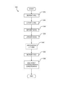
[0065] Figure 3A is a process flow, 300, in accord with methods of the
invention.
Specifically, an EC layer is deposited (on a CL, for example a TCO), see 305.
Then a CE
layer is deposited, see 310. After the EC and CE layers are deposited, then an
interfacial
region serving as an IC layer is formed therebetween, see 315. One embodiment
of the
invention is an analogous method (not depicted) where steps 305 and 310 are
reversed. The
thrust of the method being that the interfacial region, functioning as an IC
layer, is formed
after the EC and CE layers, in some embodiments using at least part of one of
the EC and CE
layers to make the interfacial region. For this reason, interfacial regions
formed in this way
are sometimes referred to as "intrinsic" IC layers. In other embodiments a
distinct layer is
formed between the EC and CE layers, for example using an oxygen-enriched
version of the
EC material or the CE material, where the layer is converted whole or in part
to the interfacial
region, but again, after formation of the EC and CE layers. Various methods to
form the
interfacial region after the EC-CE stack is formed are described below.
[0066] Thus, as mentioned, one aspect of the invention is a method of
fabricating an
electrochromic device, the method including: forming an electrochromic layer
including an
electrochromic material; forming a counter electrode layer in contact with the
electrochromic
layer without first providing an ion conducting electronically-insulating
layer between the
CA 02797826 2016-04-15
electrochromic layer and the counter electrode layer, where the counter
electrode layer
includes a counter electrode material; and forming an interfacial region
between the
electrochromic layer and the counter electrode layer, where the interfacial
region is
substantially ion conducting and substantially electronically-insulating. The
interfacial
region can contain component materials of the EC layer, the CE layer or both.
The interfacial
region can be formed in a number of ways, as described in more detail below.
[00671 Figure 3B is a process flow, 320, showing a process flow in accord with
the method
described in relation to Figure 3A, in particular, a process flow for
depositing an EC layer,
then a CE layer and ultimately forming an interfacial region, functioning as
an IC layer
therebetween. Even more particularly, in this embodiment, the EC layer
includes W03 with
various amounts of oxygen, in particular compositions and configurations; the
CE layer
includes NiWO, the interfacial region includes Li2W04, and TCO materials such
as indium
tin oxide and fluorinated tin oxide are used. It should be noted that the
layers of the
electrochromic devices are described below in terms of solid state materials.
Solid state
materials are desirable because of reliability, consistent characteristics and
process
parameters and device performance. Exemplary solid state electrochromic
devices, methods
and apparatus for making them and methods of making electrochromic windows
with such
devices are described in U.S. Published Patent Application Number
2010/0243427, entitled
"Fabrication of Low Defectivity Eleetrochromic Devices," by Kozlowski et al.,
and U.S.
Patent 8,432,603, entitled "Eleetrochromic Devices," by Wang et al. In
particular
embodiments, the electrochromic devices of the invention are all solid state
and made in
apparatus that allow deposition of one or more layers of the stack in a
controlled ambient
environment. That is, in apparatus where the layers are deposited without
leaving the
apparatus and without, for example, breaking vacuum between deposition steps,
thereby
reducing contaminants and ultimately device performance. In a particular
embodiment,
apparatus of the invention do not require a separate target for depositing an
IC layer, as is
required in conventional apparatus. As one of ordinary skill in the art would
appreciate, the
invention is not limited to these materials and methods, however, in certain
embodiments,
all of the materials making up electrochromic stacks and precursor stacks (as
described
below) are inorganic, solid (i.e., in the solid state), or both inorganic and
solid.
[0068] Because organic materials tend to degrade over time, for example when
exposed to
ultraviolet light and heat associated with window applications, inorganic
materials offer the
advantage of a reliable electrochromic stack that can function for extended
periods of time.
21
CA 02797826 2012-10-29
WO 2011/137080 PCT/US2011/033822
Materials in the solid state also offer the advantage of not having
containment and leakage
issues, as materials in the liquid state often do. It should be understood
that any one or more
of the layers in the stack may contain some amount of organic material, but in
many
implementations one or more of the layers contains little or no organic
matter. The same can
be said for liquids that may be present in one or more layers in small
amounts. It should also
be understood that solid state material may be deposited or otherwise formed
by processes
employing liquid components such as certain processes employing sol-gels or
chemical vapor
deposition.
[0069] Referring again to Figure 3B, first an EC layer of W03 is deposited,
see 325.
Figures 4A - 4C are schematic cross-sections depicting formation of
electrochromic devices
in accord with specific methods and apparatus of the invention, and
specifically in accord
with process flow 320. Specifically, Figures 4A - 4C are used to show three
non-limiting
examples of how an EC layer including W03 can be formed as part of a stack,
where an
interfacial region serving as an IC layer is formed after the other layers of
the stack are
deposited. In each of Figures 4A - 4C, the substrate 402, the first TCO layer
404, the CE
layer 410 and the second TCO layer 412 are essentially the same. Also, in each
of the three
embodiments, a stack is formed without an IC layer, and then the stack is
further processed in
order to form an interfacial region that serves as an IC layer within the
stack, that is between
the EC and the CE layer.
[0070] Referring to each of Figures 4A -4C, layered structures, 400, 403 and
409,
respectively are depicted. Each of these layered structures includes a
substrate, 402, which is,
for example, glass. Any material having suitable optical, electrical, thermal,
and mechanical
properties may be used as substrate 402. Such substrates include, for example,
glass, plastic,
and minor materials. Suitable plastic substrates include, for example acrylic,
polystyrene,
polycarbonate, allyl diglycol carbonate, SAN (styrene acrylonitrile
copolymer), poly(4-
methy1-1-pentene), polyester, polyamide, etc. and it is preferable that the
plastic be able to
withstand high temperature processing conditions. If a plastic substrate is
used, it is
preferably barrier protected and abrasion protected using a hard coat of, for
example, a
diamond-like protection coating, a silica/silicone anti-abrasion coating, or
the like, such as is
well known in the plastic glazing art. Suitable glasses include either clear
or tinted soda lime
glass, including soda lime float glass. The glass may be tempered or
untempered. In some
embodiments, commercially available substrates such as glass substrates
contain a
transparent conductive layer coating. Examples of such glasses include
conductive layer
coated glasses sold under the trademark TEC GlassTM by Pilkington of Toledo,
Ohio, and
22
CA 02797826 2012-10-29
WO 2011/137080 PCT/US2011/033822
SUNGATETm 300 and SUNGATETm 500 by PPG Industries of Pittsburgh, Pennsylvania.
TEC GlassTM is a glass coated with a fluorinated tin oxide conductive layer.
[0071] In some embodiments, the optical transmittance (i.e., the ratio of
transmitted
radiation or spectrum to incident radiation or spectrum) of substrate 402 is
about 90 to 95%,
for example, about 90-92%. The substrate may be of any thickness, as long as
it has suitable
mechanical properties to support the electrochromic device. While the
substrate 402 may be
of any size, in some embodiments, it is about 0.01 mm to 10 mm thick,
preferably about 3
mm to 9 mm thick.
[0072] In some embodiments of the invention, the substrate is architectural
glass.
Architectural glass is glass that is used as a building material.
Architectural glass is typically
used in commercial buildings, but may also be used in residential buildings,
and typically,
though not necessarily, separates an indoor environment from an outdoor
environment. In
certain embodiments, architectural glass is at least 20 inches by 20 inches,
and can be much
larger, for example, as large as about 72 inches by 120 inches. Architectural
glass is typically
at least about 2 mm thick. Architectural glass that is less than about 3.2 mm
thick cannot be
tempered. In some embodiments of the invention with architectural glass as the
substrate, the
substrate may still be tempered even after the electrochromic stack has been
fabricated on the
substrate. In some embodiments with architectural glass as the substrate, the
substrate is a
soda lime glass from a tin float line. The percent transmission over the
visible spectrum of an
architectural glass substrate (i.e., the integrated transmission across the
visible spectrum) is
generally greater than 80% for neutral substrates, but it could be lower for
colored substrates.
Preferably, the percent transmission of the substrate over the visible
spectrum is at least about
90% (for example, about 90-92%). The visible spectrum is the spectrum that a
typical human
eye will respond to, generally about 380 nm (purple) to about 780 nm (red). In
some cases,
the glass has a surface roughness of between about 10 nm and about 30 nm. In
one
embodiment, substrate 402 is soda glass with a sodium diffusion barrier (not
shown) to
prevent sodium ions from diffusing into the electrochromic device. For the
purposes of this
description, such an arrangement is referred to as "substrate 402."
[0073] Referring again to layered structures, 400, 403 and 409, on top of
substrate 402 is
deposited a first TCO layer, 404, for example made of fluorinated tin oxide or
other suitable
material, that is, among other things, conductive and transparent. Transparent
conductive
oxides include metal oxides and metal oxides doped with one or more metals.
Examples of
such metal oxides and doped metal oxides include indium oxide, indium tin
oxide, doped
indium oxide, tin oxide, doped tin oxide, zinc oxide, aluminum zinc oxide,
doped zinc oxide,
23
CA 02797826 2012-10-29
WO 2011/137080 PCT/US2011/033822
ruthenium oxide, doped ruthenium oxide and the like. In one embodiment this
second TCO
layer is between about 20 nm and about 1200 nm thick, in another embodiment,
between
about 100 nm and about 600 nm thick, in another embodiment about 350 nm thick.
The TCO
layer should have an appropriate sheet resistance (Rs) because of the
relatively large area
spanned by the layers. In some embodiments, the sheet resistance of the TCO
layers is
between about 5 and about 30 Ohms per square. In some embodiments, the sheet
resistance
of TCO layers is about 15 Ohms per square. In general, it is desirable that
the sheet
resistance of each of the two conductive layers be about the same. In one
embodiment, the
two layers, for example 404 and 412, each have a sheet resistance of about 10-
15 Ohms per
square.
[0074] Each of layered structures 400, 403 and 409, include a stack 414a, 414b
and 414c,
respectively, each of which include the first TCO layer 404 on top of
substrate 402, a CE
layer 410, and a second TCO layer 412. The difference in each of layered
structures 400, 403
and 409 is how the EC layer was formed, which in turn affects the morphology
of the
resultant interfacial region in each scenario.
[0075] Consistent with process flow 325 of Figure 3B, each of stacks 414a,
414b and 414c
include an electrochromic layer deposited on top of the first TCO layer 404.
The
electrochromic layer may contain any one or more of a number of different
electrochromic
materials, including metal oxides. Such metal oxides include tungsten oxide
(W03),
molybdenum oxide (Mo03), niobium oxide (Nb205), titanium oxide (Ti02), copper
oxide
(CA)), iridium oxide (Ir203), chromium oxide (Cr203), manganese oxide (Mn203),
vanadium
oxide (V205), nickel oxide (Ni203), cobalt oxide (Co203) and the like. In some
embodiments,
the metal oxide is doped with one or more dopants such as lithium, sodium,
potassium,
molybdenum, niobium, vanadium, titanium, and/or other suitable metals or
compounds
containing metals. Mixed oxides (for example, W-Mo oxide, W-V oxide) are also
used in
certain embodiments, that is, the electrochromic layer includes two or more of
the
aforementioned metal oxides. An electrochromic layer including a metal oxide
is capable of
receiving ions transferred from a counter electrode layer.
[0076] In some embodiments, tungsten oxide or doped tungsten oxide is used for
the
electrochromic layer. In one embodiment of the invention, the electrochromic
layer is made
substantially of WON, where "x" refers to an atomic ratio of oxygen to
tungsten in the
electrochromic layer, and x is between about 2.7 and 3.5. It has been
suggested that only sub-
stoichiometric tungsten oxide exhibits electrochromism; i.e., stoichiometric
tungsten oxide,
W03, does not exhibit electrochromism. In a more specific embodiment, WO,
where x is
24
CA 02797826 2012-10-29
WO 2011/137080 PCT/US2011/033822
less than 3.0 and at least about 2.7 is used for the electrochromic layer. In
another
embodiment, the electrochromic layer is W0x, where x is between about 2.7 and
about 2.9.
Techniques such as Rutherford Backscattering Spectroscopy (RBS) can identify
the total
number of oxygen atoms which include those bonded to tungsten and those not
bonded to
tungsten. In some instances, tungsten oxide layers where x is 3 or greater
exhibit
electrochromism, presumably due to unbound excess oxygen along with sub-
stoichiometric
tungsten oxide. In another embodiment, the tungsten oxide layer has
stoichiometric or
greater oxygen, where x is 3.0 to about 3.5. In some embodiments of the
invention, at least a
portion of the EC layer has an excess of oxygen. This more highly oxygenated
region of the
EC layer is used as a precursor to formation of an ion conducting electron
insulating region
which serves as an IC layer. In other embodiments a distinct layer of highly
oxygenated EC
material is formed between the EC layer and the CE layer for ultimate
conversion, at least in
part, to an ion conducting electronically-insulating interfacial region.
[0077] In certain embodiments, the tungsten oxide is crystalline,
nanocrystalline, or
amorphous. In some embodiments, the tungsten oxide is substantially
nanocrystalline, with
grain sizes, on average, from about 5 nm to 50 nm (or from about 5 nm to 20
nm), as
characterized by transmission electron microscopy (TEM). The tungsten oxide
morphology
or microstructure may also be characterized as nanocrystalline using x-ray
diffraction (XRD)
and/or electron diffraction, such as selected area electron diffraction
(SAED). For example,
nanocrystalline electrochromic tungsten oxide may be characterized by the
following XRD
features: a crystal size of about 10 to 100 nm, for example, about 55nm.
Further,
nanocrystalline tungsten oxide may exhibit limited long range order, for
example, on the
order of several (about 5 to 20) tungsten oxide unit cells.
[0078] Thus, for convenience, the remainder of process flow 320, in Figure 3B,
will be
further described in relation to a first embodiment, including formation of EC
layer 406,
represented in Figure 4A. Then a second and third embodiment, represented in
Figures 4B
and 4C, respectively, will be described thereafter with particular emphasis on
formation and
morphology and/or microstructure of their respective EC layers.
[0079] As mentioned with reference to Figure 3B, an EC layer is deposited, see
325. In a
first embodiment (represented in Figure 4A), a substantially homogeneous EC
layer, 406,
including W03 is formed as part of stack 414a, where the EC layer is in direct
contact with a
CE layer 410. In one embodiment, the EC layer includes W03 as described above.
In one
embodiment, heating is applied during deposition of at least a portion of the
W03. In one
particular embodiment, several passes are made past a sputter target, where a
portion of the
CA 02797826 2012-10-29
WO 2011/137080 PCT/US2011/033822
W03 is deposited on each pass, and heating is applied, for example to
substrate 402, after
each deposition pass to condition the W03 prior to deposition of the next
portion of W03 of
layer 406. In other embodiments, the W03 layer may be heated continually
during
deposition, and deposition can be done in a continuous manner, rather than
several passes
with a sputter target. In one embodiment, the EC layer is between about 300 nm
and about
600 nm thick. As mentioned, the thickness of the EC layer depends on upon the
desired
outcome and method of forming the IC layer.
[0080] In embodiments described in relation to Figure 4A, the EC layer is W03,
between
about 500 nm and about 600 nm thick, that is sputtered using a tungsten target
and a sputter
gas including between about 40% and about 80% 02 and between about 20% Ar and
about
60% Ar, and where the substrate upon which the W03 is deposited is heated, at
least
intermittently, to between about 150 C and about 450 C during formation of the
EC layer. In
a particular embodiment, the EC layer is W03, about 550 nm thick, sputtered
using the
tungsten target, where the sputter gas includes about 50% to about 60% 02 and
about 40% to
about 50% Ar, and the substrate upon which the W03 is deposited is heated, at
least
intermittently, to between about 250 C and about 350 C during formation of the
electrochromic layer. In these embodiments, the W03 layer is substantially
homogenous. In
one embodiment, the W03 is substantially polycrystalline. It is believed that
heating the
W03, at least intermittently, during deposition aids in formation of a
polycrystalline form of
the W03.
[0081] As mentioned, a number of materials are suitable for the EC layer.
Generally, in
electrochromic materials, the colorization (or change in any optical property
¨ for example,
absorbance, reflectance, and transmittance) of the electrochromic material is
caused by
reversible ion insertion into the material (for example, intercalation) and a
corresponding
injection of a charge balancing electron. Typically some fraction of the ion
responsible for
the optical transition is irreversibly bound up in the electrochromic
material. As described
herein, some or all of the irreversibly bound ions are used to compensate
"blind charge" in
the material. In most electrochromic materials, suitable ions include lithium
ions (Lit) and
hydrogen ions (H+) (i.e., protons). In some cases, however, other ions will be
suitable. These
include, for example, deuterium ions (D+), sodium ions (Na), potassium ions
(I(+), calcium
ions (Ca), barium ions (M.++), strontium ions (Sr), and magnesium ions (Mg).
In
various embodiments described herein, lithium ions are used to produce the
electrochromic
phenomena. Intercalation of lithium ions into tungsten oxide (W03_y (0 <y
¨0.3)) causes
26
CA 02797826 2012-10-29
WO 2011/137080 PCT/US2011/033822
the tungsten oxide to change from transparent (bleached state) to blue
(colored state). In a
typical process where the EC layer includes or is tungsten oxide, lithium is
deposited, for
example via sputtering, on EC layer 406 to satisfy the blind charge (as will
be discussed in
more detail below with reference to Figures 6 and 7), see 330 of the process
flow in Figure
3B. In one embodiment, the lithiation is performed in an integrated deposition
system where
vacuum is not broken between deposition steps. It should be noted that in some
embodiments, lithium is not added at this stage, but rather can be added after
deposition of
the counter electrode layer or in other embodiments lithium is added after the
TCO is
deposited.
[0082] Referring again to Figure 4A, next a CE layer, 410, is deposited on EC
layer 406.
In some embodiments, counter electrode layer 410 is inorganic and/or solid.
The counter
electrode layer may include one or more of a number of different materials
that are capable of
serving as reservoirs of ions when the electrochromic device is in the
bleached state. During
an electrochromic transition initiated by, for example, application of an
appropriate electric
potential, the counter electrode layer transfers some or all of the ions it
holds to the
electrochromic layer, changing the electrochromic layer to the colored state.
Concurrently, in
the case of NiO and/or NiWO, the counter electrode layer colors with the loss
of ions.
[0083] In some embodiments, suitable materials for the counter electrodes
include nickel
oxide (NiO), nickel tungsten oxide (NiWO), nickel vanadium oxide, nickel
chromium oxide,
nickel aluminum oxide, nickel manganese oxide, nickel magnesium oxide,
chromium oxide
(Cr203), manganese oxide (Mn02) and Prussian blue. Optically passive counter
electrodes
include cerium titanium oxide (Ce02-Ti02), cerium zirconium oxide (Ce02-Zr02),
nickel
oxide (NiO), nickel-tungsten oxide (NiWO), vanadium oxide (V205), and mixtures
of oxides
(for example, a mixture of Ni203 and W03). Doped formulations of these oxides
may also be
used, with dopants including, for example, tantalum and tungsten. Because
counter electrode
layer 410 contains the ions used to produce the electrochromic phenomenon in
the
electrochromic material when the electrochromic material is in the bleached
state, the counter
electrode preferably has high transmittance and a neutral color when it holds
significant
quantities of these ions. The counter electrode morphology may be
crystalline,
nanocrystalline, or amorphous.
[0084] In some embodiments, where the counter electrode layer is nickel-
tungsten oxide,
the counter electrode material is amorphous or substantially amorphous.
Substantially
amorphous nickel-tungsten oxide counter electrodes have been found to perform
better, under
some conditions, in comparison to their crystalline counterparts. The
amorphous state of the
27
CA 02797826 2012-10-29
WO 2011/137080 PCT/US2011/033822
nickel-tungsten oxide may be obtained though the use of certain processing
conditions,
described below. While not wishing to be bound to any theory or mechanism, it
is believed
that amorphous nickel-tungsten oxide is produced by relatively higher energy
atoms in the
sputtering process. Higher energy atoms are obtained, for example, in a
sputtering process
with higher target powers, lower chamber pressures (i.e., higher vacuum), and
smaller source
to substrate distances. Under the described process conditions, higher density
films, with
better stability under UV/heat exposure are produced.
[0085] In certain embodiments, the amount of nickel present in the nickel-
tungsten oxide
can be up to about 90% by weight of the nickel tungsten oxide. In a specific
embodiment, the
mass ratio of nickel to tungsten in the nickel tungsten oxide is between about
4:6 and 6:4, in
one example, about 1:1. In one embodiment, the NiWO is between about 15%
(atomic) Ni
and about 60% Ni, and between about 10% W and about 40% W. In another
embodiment,
the NiWO is between about 30% (atomic) Ni and about 45% Ni, and between about
15% W
and about 35% W. In another embodiment, the NiWO is between about 30% (atomic)
Ni and
about 45% Ni, and between about 20% W and about 30% W. In one embodiment, the
NiWO
is about 42% (atomic) Ni and about 14% W.
[0086] In one embodiment, CE layer 410 is NiWO as described above, see 335 of
Figure
3B. In one embodiment, the CE layer is between about 150 nm and about 300 nm
thick, in
another embodiment between about 200 nm and about 250 nm thick, in another
embodiment
about 230 nm thick.
[0087] In a typical process, lithium is also applied to the CE layer until the
CE layer is
bleached. It should be understood that reference to a transition between a
colored state and
bleached state is non-limiting and suggests only one example, among many, of
an
electrochromic transition that may be implemented. Unless otherwise specified
herein,
whenever reference is made to a bleached-colored transition, the corresponding
device or
process encompasses other optical state transitions such non-reflective-
reflective, transparent-
opaque, etc. Further the term "bleached" refers to an optically neutral state,
for example,
uncolored, transparent or translucent. Still further, unless specified
otherwise herein, the
"color" of an electrochromic transition is not limited to any particular
wavelength or range of
wavelengths. As understood by those of skill in the art, the choice of
appropriate
electrochromic and counter electrode materials governs the relevant optical
transition.
[0088] In a particular embodiment, lithium, for example via sputtering, is
added to a
NiWO CE layer, see 340 of Figure 3B. In a particular embodiment, an additional
amount of
lithium is added after sufficient lithium has been introduced to fully bleach
the NiWO, see
28
CA 02797826 2012-10-29
WO 2011/137080 PCT/US2011/033822
345 of Figure 3B (this process is optional, and in one embodiment excess
lithium is not added
at this stage in the process). In one embodiment this additional amount is
between about 5%
and about 15% excess based on the quantity required to bleach the counter
electrode layer. In
another embodiment, the excess lithium added to the CE layer is about 10%
excess based on
the quantity required to bleach the counter electrode layer. After CE layer
410 is deposited,
bleached with lithium and additional lithium is added, a second TCO layer,
412, is deposited
on top of the counter electrode layer, see 350 of Figure 3B. In one
embodiment, the
transparent conducting oxide includes indium tin oxide, in another embodiment
the TCO
layer is indium tin oxide. In one embodiment this second TCO layer is between
about 20 nm
and about 1200 nm thick, in another embodiment, between about 100 nm and about
600 nm
thick, in another embodiment about 350 nm thick.
[0089] Referring again to Figure 4A, once layered structure 400 is complete,
it is subjected
to thermochemical conditioning which converts at least a portion of stack 414a
to an IC layer
(if it was not already converted due to lithium diffusion or other mechanism).
Stack 414a is a
precursor, not an electrochromic device, because it does not yet have an ion
conducting/electronically-insulating layer (or region) between EC layer 406
and CE layer
410. In this particular embodiment, in a two step process, a portion of EC
layer 406 is
converted to IC layer 408 to make a functional electrochromic device 401.
Referring to
Figure 3B, layered structure 400 is subjected to an MTCC, see 355. In one
embodiment, the
stack is first subjected to heating, under inert atmosphere (for example
argon) at between
about 150 C and about 450 C, for between about 10 minutes and about 30
minutes, and then
for between about 1 minutes and about 15 minutes under 02. In another
embodiment, the
stack is heated at about 250 C, for about 15 minutes under inert atmosphere,
and then about 5
minutes under 02. Next, layered structure 400 is subjected to heating in air.
In one
embodiment the stack is heated in air at between about 250 C and about 350 C,
for between
about 20 minutes and about 40 minutes; in another embodiment the stack is
heated in air at
about 300 C for about 30 minutes. The energy required to implement MTCC need
not be
radiant heat energy. For example, in one embodiment ultraviolet radiation is
used to
implement MTCC. Other sources of energy could also be used without escaping
the scope of
the invention.
[0090] After the multistep thermochemical conditioning, process flow 320 is
complete and
a functional electrochromic device is created. As mentioned, and while not
wishing to be
bound by theory, it is believed that the lithium in stack 414a along with a
portion of EC layer
406 and/or CE layer 410 combine to form interfacial region 408 which functions
as an IC
29
CA 02797826 2012-10-29
WO 2011/137080 PCT/US2011/033822
layer. Interfacial region 408 is believed to be primarily lithium tungstate,
Li2W04, which is
known to have good ion conducting and electronically-insulating properties
relative to
traditional IC layer materials. As discussed above, precisely how this
phenomenon occurs is
not yet known. There are chemical reactions that must take place during the
multistep
thermochemical conditioning to form the ion conducting electronically-
insulating region 408
between the EC and CE layers, but also it is thought that an initial flux of
lithium traveling
through the stack, for example provided by the excess lithium added to the CE
layer as
described above, plays a part in formation of IC layer 408. The thickness of
the ion
conducting electronically-insulating region may vary depending on the
materials employed
and process conditions for forming the layer. In some embodiments, interfacial
region 408 is
about 10 nm to about 150 nm thick, in another embodiment about 20 nm to about
100 nm
thick, and in other embodiments between about 30 nm to about 50 nm thick.
[0091] As mentioned above, there are a number of suitable materials for making
the EC
layer. As such, using, for example lithium or other suitable ions, in the
methods described
above one can make other interfacial regions that function as IC layers
starting from oxygen
rich EC materials. Suitable EC materials for this purpose include, but are not
limited to 5i02,
Nb205, Ta205, Ti02, Zr02 and Ce02. In particular embodiments where lithium
ions are used,
ion conducting materials such as but not limited to, lithium silicate, lithium
aluminum
silicate, lithium aluminum borate, lithium aluminum fluoride, lithium borate,
lithium nitride,
lithium zirconium silicate, lithium niobate, lithium borosilicate, lithium
phosphosilicate, and
other such lithium-based ceramic materials, silicas, or silicon oxides,
including lithium
silicon-oxide can be made as interfacial regions that function as IC layers.
[0092] As mentioned, in one embodiment, the precursor of the ion conducting
region is an
oxygen-rich (super-stoichiometric) layer that is transformed into ion-
conducting/electron-
insulating region via lithiation and MTCC as described herein. While not
wishing to be
bound to theory, it is believed that upon lithiation, the excess oxygen forms
lithium oxide,
which further forms lithium salts, that is, lithium electrolytes, such as
lithium tungstate
(Li2W04), lithium molybdate (Li2Mo04), lithium niobate (LiNb03), lithium
tantalate
(LiTa03), lithium titanate (Li2TiO3), lithium zirconate (Li2Zr03) and the
like. In one
embodiment, the interfacial region comprises at least one of tungsten oxide
(W03+, 0 < x <
1.5), molybdenum oxide (Mo03,, 0 < x < 1.5), niobium oxide (Nb205+x, 0 < x <
2), titanium
oxide (Ti02+x, 0 < x < 1.5), tantalum oxide (Ta205+õ , 0 < x < 2), zirconium
oxide (Zr02+õ, 0
< x <1.5) and cerium oxide (Ce02+õ, 0 < x < 1.5).
CA 02797826 2012-10-29
WO 2011/137080 PCT/US2011/033822
[0093] Any material, however, may be used for the ion conducting interfacial
region
provided it can be fabricated with low defectivity and it allows for the
passage of ions
between the counter electrode layer 410 to the electrochromic layer 406 while
substantially
preventing the passage of electrons. The material may be characterized as
being substantially
conductive to ions and substantially resistive to electrons. In one
embodiment, the ion
conductor material has an ionic conductivity of between about 10-1 Siemens/cm
(or ohm-
lcm-1) and about 10-3 Siemens/cm and an electronic resistivity of greater than
105 ohms-cm.
In another embodiment, the ion conductor material has an ionic conductivity of
between
about 10-8 Siemens/cm and about 10-3 Siemens/cm and an electronic resistivity
of greater
than 1010 ohms-cm. While ion conducting layers should generally resist leakage
current (for
example, providing a leakage current of not more than about 15 A/cm2, it has
been found
that some devices fabricated as described herein have surprising high leakage
currents, for
example, between about 40 A/cm and about 150 A/cm, yet provide good color
change
across the device and operate efficiently.
[0094] As mentioned above, there are at least two other ways of creating an
ion conducting
electronically-insulating region between the EC and CE layers, after formation
of the stack.
These additional embodiments are described below with reference to a
particular example
where tungsten oxide is used for the EC layer. Also, as mentioned above, the
interfacial
region with IC properties may form in situ during fabrication of the stack
when, for example,
lithium diffusion or heat converts some of the EC and/or CE layer to the
interfacial region.
[0095] In general, there are certain benefits to creating the ion conducting
region later in
the process. First, the ion conducting material may be protected from some of
the harsh
processing that occurs during deposition and lithiation of the EC and CE
layers. For
example, the deposition of these layers by a plasma process is often
accompanied by a large
voltage drop proximate the stack, frequently in the neighborhood of 15-20
volts. Such large
voltages can damage or cause break down of the sensitive ion conducting
material. By
shifting the IC material formation to later in the process, the material is
not exposed to
potentially damaging voltage extremes. Second, by forming the IC material
later in the
process, one may have better control over some process conditions that are not
possible prior
to completion of both the EC and CE layers. These conditions include lithium
diffusion and
current flow between electrodes. Controlling these and other conditions late
in the process
provides additional flexibility to tailor the physical and chemical properties
of the IC material
to particular applications. Thus, not all of the benefits of the invention are
due to the unique
31
CA 02797826 2012-10-29
WO 2011/137080 PCT/US2011/033822
interfacial region acting as an IC layer, that is, there are manufacturing and
other benefits as
well.
[0096] It has been observed that ion conducting materials formed in accordance
with some
of the embodiments described herein have superior performance when compared to
devices
fabricated using conventional techniques for forming an IC layer (for example,
PVD from an
IC material target). The device switching speed, for example, has been found
to be very fast,
for example less than 10 minutes, in one example about eight minutes, to
achieve about 80%
of end state compared to 20-25 minutes or more for traditional devices. In
some instances,
devices described herein have switching speeds orders of magnitude better than
conventional
devices. This is possibly attributable to the greater amounts of readily
transferable lithium
disposed in the interfacial region and/or the graded interfaces, for example
between the EC
and interfacial region and/or between the CE and the interfacial region. Such
lithium may be
in the EC and/or CE phases intermixed with the IC phase present in the
interfacial region. It
is also due possibly to the relatively thin layer or network of IC material
present in the
interfacial region. In support of this view, it has been observed that some
devices fabricated
in accordance with the teachings herein have high leakage currents, yet
surprisingly exhibit
good color change and good efficiency. In some cases, the leakage current
density of solidly
performing devices has been found to be at least about 100 A/cm.
[0097] Referring now to Figure 4B, in a second embodiment, the initially laid
down EC
material of stack 414b is really two layers: a first W03 layer, 406, analogous
to layer 406 in
Figure 4A, but between about 350 nm and about 450 nm thick, that is sputtered
using a
tungsten target and a first sputter gas including between about 40% and about
80% 02 and
between about 20% Ar and about 60% Ar, and a second W03 layer, 405, between
about 100
nm and about 200 nm thick, that is sputtered using the tungsten target and a
second sputter
gas including between about 70% and 100% 02 and between 0% Ar and about 30%
Ar. In
this embodiment, heat is applied, for example by heating substrate 402, at
least intermittently,
to between about 150 C and about 450 C during deposition of the first W03
layer, 406, but
not, or substantially not, heated during deposition of the second W03 layer
405. In a more
specific embodiment, layer 406 is about 400 nm thick and the first sputter gas
includes
between about 50% and about 60% 02 and between about 40% and about 50% Ar; the
second
W03 layer 405 is about 150 nm thick and the second sputter gas is
substantially pure 02. In
this embodiment, heat is applied, at least intermittently, to between about
200 C and about
350 C during formation of the first W03 layer, 406, but not, or substantially
not, heated
32
CA 02797826 2012-10-29
WO 2011/137080 PCT/US2011/033822
during formation of the second W03 layer 405. In this way, the first WO 1
layer is
substantially polycrystalline, while the second W03 layer is not necessarily
so.
[0098] Referring again to Figure 4B, as described above in relation to Figure
3B and 4A,
the stack is completed by lithiation of EC layer(s) 406 and 405 to
approximately or
substantially satisfy the blind charge, deposition of CE layer 410, lithiation
of the CE layer to
bleach state, addition of additional lithium, and deposition of the second TCO
layer 412 to
complete layered stack 403. Analogous thermochemical conditioning is performed
on
layered stack 403 to provide layered stack 407, a functional electrochromic
device including
an ion conducting electronically-insulating region 408a. While not wishing to
be bound by
theory, in this example, it is believed that the oxygen rich layer 405 of W03
serves primarily
as the source of precursor material to form interfacial region 408a. In this
example, the entire
oxygen rich W03 layer is depicted as converting to interfacial region 408a,
however it has
been found that this is not always the case. In some embodiments, only a
portion of an
oxygen rich layer is converted to form an interfacial region that serves the
function of an IC
layer.
[0099] Referring now to Figure 4C, in a third embodiment, layered stack 409
includes an
EC layer, 406a, which has a graded composition of W03 and is formed as part of
a stack,
414c, where the graded composition includes varying levels of oxygen. In one
non-limiting
example, there is a higher concentration of oxygen in EC layer 406a at the EC-
CE layer (410)
interface than, for example, at the interface of TCO layer 404 with EC layer
406a.
[0100] In one embodiment, EC layer 406a is a graded composition W03 layer,
between
about 500 nm and about 600 nm thick, that is sputtered using a tungsten target
and a sputter
gas, where the sputter gas includes between about 40% and about 80% 02 and
between about
20% Ar and about 60% Ar at the start of sputtering the electrochromic layer,
and the sputter
gas includes between about 70% and 100% 02 and between 0% Ar and about 30% Ar
at the
end of sputtering the electrochromic layer, and where heat is applied, for
example to substrate
402, at least intermittently, to between about 150 C and about 450 C at the
beginning of
formation of EC layer 406a but not, or substantially not, applied during
deposition of at least
a final portion of EC layer 406a. In a more specific embodiment, the graded
composition
W03 layer is about 550 nm thick; the sputter gas includes between about 50%
and about 60%
02 and between about 40% and about 50% Ar at the start of sputtering the
electrochromic
layer, and the sputter gas is substantially pure 02 at the end of sputtering
the electrochromic
layer; and where heat is applied, for example to substrate 402, at least
intermittently, to
between about 200 C and about 350 C at the beginning of formation of the
electrochromic
33
CA 02797826 2012-10-29
WO 2011/137080 PCT/US2011/033822
layer but not, or substantially not, applied during deposition of at least a
final portion of the
electrochromic layer. In one embodiment heat is applied at the described
temperature ranges
at the onset of deposition and gradually decreased to no applied heat at a
point where about
half of the EC layer is deposited, while the sputter gas composition is
adjusted from between
about 50% and about 60% 02 and between about 40% and about 50% Ar to
substantially pure
02 along a substantially linear rate during deposition of the EC layer.
[0101] More generally, the interfacial region typically, though not
necessarily, has a
heterogeneous structure that includes at least two discrete components
represented by
different phases and/or compositions. Further, the interfacial region may
include a gradient
in these two or more discrete components such as an ion conducting material
and an
electrochromic material (for example, a mixture of lithium tungstate and
tungsten oxide).
The gradient may provide, for example, a variable composition, microstructure,
resistivity,
dopant concentration (for example, oxygen concentration), stoichiometry,
density, and/or
grain size regime. The gradient may have many different forms of transition
including a
linear transition, a sigmoidal transition, a Gaussian transition, etc. In one
example, an
electrochromic layer includes a tungsten oxide region that transitions into a
superstoichiometric tungsten oxide region. Part or all of the
superstoichiometric oxide region
is converted to the interfacial region. In the final structure, the tungsten
oxide region is
substantially polycrystalline and the microstructure transitions to
substantially amorphous at
the interfacial region. In another example, an electrochromic layer includes a
tungsten oxide
region that transitions into a niobium (superstoichiometric) oxide region.
Part or all of the
niobium oxide region is converted to the interfacial region. In the final
structure, the tungsten
oxide region is substantially polycrystalline and the microstructure
transitions to substantially
amorphous at the interfacial region.
[0102] Referring again to Figure 4C, as described above in relation to Figures
3B and 4A,
the stack is completed by lithiation of EC layer 406a to approximately or
substantially
satisfy the blind charge, deposition of CE layer 410, lithiation of the CE
layer to bleach state,
addition of additional lithium, and deposition of the second TCO layer 412 to
complete
layered stack 409. Analogous multistep thermochemical conditioning is
performed on
layered stack 409 to provide layered stack 411, a functional electrochromic
device including
an ion conducting electronically-insulating region 408b and at least a portion
of original
graded EC layer 406a which serves as the EC layer in the functional
electrochromic device
411. While not wishing to be bound by theory, in this example, it is believed
that uppermost
oxygen rich portion of the graded layer of W03 primarily forms graded
interfacial region
34
CA 02797826 2012-10-29
WO 2011/137080 PCT/US2011/033822
408b. While not wishing to be bound by theory, there is the possibility that
formation of the
interfacial region is self-limiting and depends on relative amounts of oxygen,
lithium,
electrochromic material and/or counter electrode material in the stack.
[0103] In various embodiments described herein, the electrochromic stack is
described as
not, or substantially not, being heated during certain processing phases. In
one embodiment,
the stack is cooled, actively or passively (for example using a heat sink),
after a heating step.
Apparatus of the invention include active and passive cooling components, for
example,
active cooling can include platens that are cooled via fluid circulation,
cooling via exposure
to cooled (e.g. via expansion) gases, refrigeration units and the like.
Passive cooling
components can include heat sinks, such as blocks of metal and the like, or
simply removing
the substrate from exposure to heat.
[0104] Another aspect of the invention is a method of fabricating an
electrochromic device,
the method including: (a) forming either an electrochromic layer including an
electrochromic
material or a counter electrode layer including a counter electrode material;
(b) forming an
intermediate layer over the electrochromic layer or the counter electrode
layer, where the
intermediate layer includes an oxygen rich form of at least one of the
electrochromic
material, the counter electrode material and an additional material, where the
additional
material includes distinct electrochromic or counter electrode material, where
the
intermediate layer is not substantially electronically-insulating; (c) forming
the other of the
electrochromic layer and the counter electrode layer; and (d) allowing at
least a portion of the
intermediate layer to become substantially electronically-insulating. In one
embodiment, the
electrochromic material is W03. In another embodiment, (a) includes sputtering
W03 using a
tungsten target and a first sputter gas including between about 40% and about
80% 02 and
between about 20% Ar and about 60% Ar, to reach of thickness of between about
350 nm and
about 450 nm, and heating, at least intermittently, to between about 150 C and
about 450 C
during formation of the electrochromic layer. In another embodiment, (b)
includes sputtering
W03 using a tungsten target and a second sputter gas including between about
70% and
100% 02 and between 0% Ar and about 30% Ar, to reach a thickness of between
about 100
nm and about 200 nm, without heating. In yet another embodiment, the method
further
includes sputtering lithium onto the intermediate layer until the blind charge
is approximately
or substantially satisfied. In one embodiment, the counter electrode layer
includes NiWO,
between about 150 nm and about 300 nm thick. In another embodiment, lithium is
sputtered
onto counter electrode layer until the counter electrode layer is bleached. In
another
embodiment, an additional amount of lithium, between about 5% and about 15%
excess
CA 02797826 2012-10-29
WO 2011/137080 PCT/US2011/033822
based on the quantity required to bleach the counter electrode layer, is
sputtered onto the
counter electrode layer. In another embodiment, a transparent conducting oxide
layer is
deposited on top of the counter electrode layer. In one embodiment the
transparent
conducting oxide includes indium tin oxide, in another embodiment, the
transparent
conducting oxide is indium tin oxide. In another embodiment, the stack formed
from the
above embodiments is heated at between about 150 C and about 450 C, for
between about 10
minutes and about 30 minutes under Ar, and then for between about 1 minutes
and about 15
minutes under 02, and then heated in air at between about 250 C and about 350
C, for
between about 20 minutes and about 40 minutes.
[0105] In another embodiment, (a) includes sputtering a first electrochromic
material of
formula M0x, where M is a metal or metalloid element and x indicates
stoichiometric oxygen
to M ratio, and (b) includes sputtering a second electrochromic material of
formula NOy as
the intermediate layer, where N is the same or a different metal or metalloid
element and y
indicates a superstoichiometric amount of oxygen to N ratio. In one
embodiment, M is
tungsten and N is tungsten. In another embodiment, M is tungsten and N is
selected from the
group consisting of niobium, silicon, tantalum, titanium, zirconium and
cerium.
[0106] Another embodiment of the invention is an electrochromic device
including: (a) an
electrochromic layer including an electrochromic material; (b) a counter
electrode layer
including a counter electrode material; and (c) an interfacial region between
the
electrochromic layer and the counter electrode layer, where the interfacial
region includes an
electronically-insulating ion conducting material and at least one of the
electrochromic
material, the counter electrode material and an additional material, where the
additional
material includes distinct electrochromic or counter electrode material.
[0107] In one embodiment, the electronically-insulating ion conducting
material and at
least one of the electrochromic material, the counter electrode material and
the additional
material are substantially evenly distributed within the interfacial region.
In another
embodiment, the electronically-insulating ion conducting material and at least
one of the
electrochromic material, the counter electrode material and the additional
material include a
composition gradient in a direction perpendicular to the layers. In another
embodiment,
consistent with either of the two aforementioned embodiments, the
electronically-insulating
ion conducting material includes lithium tungstate, the electrochromic
material includes a
tungsten oxide and the counter electrode material includes nickel tungsten
oxide. In a
specific implementation of the aforementioned embodiment, there is no
additional material.
In one embodiment, the electrochromic layer is between about 300 nm and about
500 rim
36
CA 02797826 2012-10-29
WO 2011/137080 PCT/US2011/033822
thick, the interfacial region is between about 10 nm and about 150 nm thick,
and the counter
electrode layer is between about 150 nm and about 300 nm thick. In another
embodiment,
the electrochromic layer is between about 400 nm and about 500 nm thick; the
interfacial
region is between about 20 nm and about 100 nm thick, and the counter
electrode layer is
between about 150 and about 250 nm thick. In yet another embodiment, the
electrochromic
layer is between about 400 nm and about 450 nm thick; the interfacial region
is between
about 30 nm and about 50 nm thick, and the counter electrode layer is about
200 nm and
about 250 nm thick.
[0108] Another embodiment is a method of fabricating an electrochromic device,
the
method including: depositing an electrochromic layer by sputtering a tungsten
target with a
sputter gas comprising between about 40% and about 80% 02 and between about
20% Ar and
about 60% Ar to produce W03 to a thickness of between about 500 nm and about
600 nm,
where the substrate upon which the W01 is deposited is heated, at least
intermittently, to
between about 150 C and about 450 C during formation of the electrochromic
layer;
sputtering lithium onto the electrochromic layer until the blind charge is
satisfied; depositing
a counter electrode layer on the electrochromic layer without first providing
an ion
conducting electronically-insulating layer between the electrochromic layer
and the counter
electrode layer, where the counter electrode layer includes NiWO; sputtering
lithium onto the
counter electrode layer until the counter electrode layer is substantially
bleached; and forming
an interfacial region between the electrochromic layer and the counter
electrode layer, where
the interfacial region is substantially ion conducting and substantially
electronically-
insulating. In one embodiment, forming the interfacial region includes MTCC of
the stack,
alone or along with substrate, conductive and/or encapsulation layers.
[0109] The electrochromic devices of the invention can include one or more
additional
layers (not shown) such as one or more passive layers, for example to improve
certain optical
properties, providing moisture or scratch resistance, to hermetically seal the
electrochromic
device and the like. Typically, but not necessarily, a capping layer is
deposited on the
electrochromic stack. In some embodiments, the capping layer is SiA10. In some
embodiments, the capping layer is deposited by sputtering. In one embodiment,
the thickness
of a capping layer is between about 30 nm and about 100 nm.
[0110] From the discussion above, it should be appreciated that electrochromic
devices of
the invention can be made in a single chamber apparatus, for example a sputter
tool, that has,
for example, a tungsten target, a nickel target and a lithium target along
with oxygen and
argon sputter gases. As mentioned, due to the nature of the interfacial
regions formed to
37
CA 02797826 2012-10-29
WO 2011/137080 PCT/US2011/033822
serve the purpose of a conventional distinct IC layer, a separate target for
sputtering an IC
layer is not necessary. Of particular interest to the inventors is fabricating
electrochromic
devices of the invention, for example, in a high throughput fashion, therefore
it is desirable to
have apparatus that can fabricate electrochromic devices of the invention
sequentially as
substrates pass through an integrated deposition system. For example, the
inventors are
particularly interested in fabricating electrochromic devices on windows,
particularly
architectural glass scale windows (supra).
[0111] Thus, another aspect of the invention is an apparatus for fabricating
an
electrochromic device, including: an integrated deposition system including:
(i) a first
deposition station containing a material source configured to deposit an
electrochromic layer
including an electrochromic material; and (ii) a second deposition station
configured to
deposit a counter electrode layer including a counter electrode material; and
a controller
containing program instructions for passing the substrate through the first
and second
deposition stations in a manner that sequentially deposits a stack on the
substrate, the stack
having an intermediate layer sandwiched in between the electrochromic layer
and the counter
electrode layer; where either or both of the first deposition station and the
second deposition
station are also configured to deposit the intermediate layer over the
electrochromic layer or
the counter electrode layer, and where the intermediate layer includes an
oxygen rich form of
the electrochromic material or the counter electrode material and where the
first and second
deposition stations are interconnected in series and operable to pass a
substrate from one
station to the next without exposing the substrate to an external environment.
In one
embodiment, apparatus of the invention are operable to pass the substrate from
one station to
the next without breaking vacuum and may include one or more lithiation
stations operable to
deposit lithium from a lithium-containing material source on one or more
layers of the
electrochromic device. In one embodiment, apparatus of the invention are
operable to
deposit the electrochromic stack on an architectural glass substrate.
[0112] In one embodiment, the apparatus is operable to pass the substrate from
one station
to the next without breaking vacuum. In another embodiment, the integrated
deposition
system further includes one or more lithiation stations operable to deposit
lithium from a
lithium-containing material source on at least one of the electrochromic
layer, the
intermediate layer and the counter electrode layer. In yet another embodiment,
the integrated
deposition system is operable to deposit the stack on an architectural glass
substrate. In
another embodiment, the integrated deposition system further includes a
substrate holder and
transport mechanism operable to hold the architectural glass substrate in a
vertical orientation
38
CA 02797826 2012-10-29
WO 2011/137080 PCT/US2011/033822
while passing through the integrated deposition system. In another embodiment,
the
apparatus further includes one or more load locks for passing the substrate
between an
external environment and the integrated deposition system. In another
embodiment, the
apparatus further includes at least one slit valve operable to permit
isolation of the one or
more lithium deposition stations from at least one of the first deposition
station and the
second deposition station. In one embodiment, the integrated deposition system
includes one
or more heaters configured to heat the substrate.
[0113] Figure 5 depicts a simplified representation of an integrated
deposition system 500
in a perspective view and with more detail including a cutaway view of the
interior. In this
example, system 500 is modular, where entry load lock 502 and exit load lock
504 arc
connected to deposition module 506. There is an entry port, 510, for loading,
for example,
architectural glass substrate 525 (load lock 504 has a corresponding exit
port). Substrate 525
is supported by a pallet, 520, which travels along a track, 515. In this
example, pallet 520 is
supported by track 515 via hanging but pallet 520 could also be supported atop
a track
located near the bottom of apparatus 500 or a track, for example mid-way
between top and
bottom of apparatus 500. Pallet 520 can translate (as indicated by the double
headed arrow)
forward and/or backward through system 500. For example during lithium
deposition, the
substrate may be moved forward and backward in front of a lithium target, 530,
making
multiple passes in order to achieve a desired lithiation. This function is not
limited to lithium
targets, however, for example a tungsten target may pass multiple times past a
substrate, or
the substrate may pass by via forward/backward motion path in front of the
tungsten target to
deposit, for example, an electrochromic layer. Pallet 520 and substrate 525
are in a
substantially vertical orientation. A substantially vertical orientation is
not limiting, but it
may help to prevent defects because particulate matter that may be generated,
for example,
from agglomeration of atoms from sputtering, will tend to succumb to gravity
and therefore
not deposit on substrate 525. Also, because architectural glass substrates
tend to be large, a
vertical orientation of the substrate as it traverses the stations of the
integrated deposition
system enables coating of thinner glass substrates since there are less
concerns over sag that
occurs with thicker hot glass.
[0114] Target 530, in this case a cylindrical target, is oriented
substantially parallel to and
in front of the substrate surface where deposition is to take place (for
convenience, other
sputter means are not depicted here). Substrate 525 can translate past target
530 during
deposition and/or target 530 can move in front of substrate 525. The movement
path of target
530 is not limited to translation along the path of substrate 525. Target 530
may rotate along
39
CA 02797826 2016-04-15
an axis through its length, translate along the path of the substrate (forward
and/or backward),
translate along a path perpendicular to the path of the substrate, move in a
circular path in a
plane parallel to substrate 525, etc. Target 530 need not be cylindrical, it
can be planar or any
shape necessary for deposition of the desired layer with the desired
properties. Also, there
may be more than one target in each deposition station and/or targets may move
from station
to station depending on the desired process. The various stations of an
integrated deposition
system of the invention may be modular, but once connected, form a continuous
system
where a controlled ambient environment is established and maintained in order
to process
substrates at the various stations within the system.
[0115] More detailed aspects of how electrochromic materials are deposited
using
integrated deposition system 500 are described in US Published Patent
Application
2010/0243427, US Patent 8,432,603, supra.
[0116] Integrated deposition system 500 also has various vacuum pumps, gas
inlets,
pressure sensors and the like that establish and maintain a controlled ambient
environment
within the system. These components are not shown, but rather would be
appreciated by one
of ordinary skill in the art. System 500 is controlled, for example, via a
computer system or
other controller, represented in Figure 5 by an LCD and keyboard, 535. One of
ordinary skill
in the art would appreciate that embodiments of the present invention may
employ various
processes involving data stored in or transferred through one or more computer
systems.
Embodiments of the present invention also relate to the apparatus, such
computers and
microcontrollers, for performing these operations. These apparatus and
processes may be
employed to deposit electrochromic materials of methods of the invention and
apparatus
designed to implement them. The control apparatus of this invention may be
specially
constructed for the required purposes, or it may be a general-purpose computer
selectively
activated or reconfigured by a computer program and/or data structure stored
in the computer.
The processes presented herein are not inherently related to any particular
computer or other
apparatus. In particular, various general-purpose machines may be used with
programs
written in accordance with the teachings herein, or it may be more convenient
to construct a
more specialized apparatus to perform and/or control the required method and
processes.
[0117] From the description above, particularly of Figures 3A-3B, it can be
seen that with
methods of the invention, one can not only make electrochromic devices, but
also
prefabricate a layered stack, for example 400, 403 and 409, that can in some
cases be
converted through subsequent processing, for example as described herein, to
an
electrochromic device. Though not functional electrochromic devices, by virtue
of not
CA 02797826 2012-10-29
WO 2011/137080 PCT/US2011/033822
having an ion conducting and electronically-insulating region between the EC
and CE layers,
such "electrochromic device precursors" can be of particular value. This is
especially true if
the device precursors are manufactured in a high purity, integrated processing
apparatus as
described herein, where the material layers are all deposited under a
controlled ambient
environment where, for example, vacuum is never broken. In that way, high
purity, low-
defect materials are stacked and essentially "sealed," for example, by the
final TCO layer
and/or a capping layer prior to leaving the integrated system.
[0118] Like the electrochromic devices of the invention described above,
electrochromic
device precursors can also include one or more additional layers (not shown)
such as one or
more passive layers, for example to improve certain optical properties,
providing moisture or
scratch resistance, to hermetically seal the device precursor and the like. In
one embodiment,
a capping layer is deposited on the TCO layer of the precursor stack. In some
embodiments,
the capping layer is SiA10. In some embodiments, the capping layer is
deposited by
sputtering. In one embodiment, the thickness of a capping layer is between
about 30 nm and
about 100 nm. Subsequent processing with the cap layer in place forms the IC
layer without
contamination from the environment, that is, with the additional protection of
the capping
layer.
[0119] Conversion to the functional electrochromic device can occur outside
the integrated
system if desired, since the internal stack structure is protected from the
outside environment
and somewhat less stringent purity conditions are necessary for the last
conditioning steps to
convert the precursor stack to the functional device. Such stacked
electrochromic device
precursors can have advantages, for example, longer lifespan due to conversion
to the
electrochromic device only when needed, flexibility by having, for example, a
single
precursor stack that can be stored and used when conversion parameters are
improved or fed
to different conversion chambers and/or customer sites for conversion
depending on the
needs of the final product and quality standards that must be met. Also such
precursor stacks
are useful for testing purposes, for example, quality control or research
efforts.
[0120] Accordingly, one embodiment of the invention is an electrochromic
device
precursor including: (a) a substrate; (b) a first transparent conducting oxide
layer on the
substrate; (c) a stack on the first transparent conducting oxide layer, the
stack including: (i) an
electrochromic layer including an electrochromic material, and (ii) a counter
electrode layer
including a counter electrode material; where the stack does not include an
ion conducting
and electronically-insulating region between the electrochromic layer and the
counter
electrode layer; and (d) a second transparent conducting oxide layer on top of
the stack. In
41
CA 02797826 2012-10-29
WO 2011/137080 PCT/US2011/033822
one embodiment, the electrochromic layer includes tungsten oxide and the
counter electrode
layer comprises nickel tungsten oxide. In one embodiment, at least one of the
stack and the
electrochromic layer contain lithium. In another embodiment, the
electrochromic layer is
tungsten oxide with a superstoichiometric oxygen content at least at the
interface with the
counter electrode layer. In another embodiment, the stack includes an IC
precursor layer
between the counter electrode layer and the electrochromic layer, the IC
precursor layer
including tungsten oxide with a higher oxygen content than that of the
electrochromic layer.
In one embodiment, where there is no IC precursor layer between the EC and CE
layers, the
electrochromic layer is between about 500 nm and about 600 nm thick and the
counter
electrode layer is between about 150 nm and about 300 nm thick. In another
embodiment,
where there is an IC precursor layer between the EC and CE layers, the
electrochromic layer
is between about 350 nm and about 400 nm thick, the IC precursor layer is
between about 20
nm and about 100 nm thick, and the counter electrode layer is between about
150 nm and
about 300 nm thick. In one embodiment, precursor devices described herein are
exposed to
heating to convert them to functional electrochromic devices. In one
embodiment, the
heating is part of an MTCC.
[0121] Another embodiment is an electrochromic device including: (a) an
electrochromic
layer including an electrochromic material, and (b) a counter electrode layer
including a
counter electrode material, where the device does not contain a
compositionally
homogeneous layer of electronically-insulating, ion conducting material
between the
electrochromic layer and the counter electrode layer. In one embodiment, the
electrochromic
material is tungsten oxide, the counter electrode material is nickel tungsten
oxide, and
between the electrochromic layer and the counter electrode layer is an
interfacial region
including a mixture of lithium tungstate and at least one of tungsten oxide
and nickel tungsten
oxide. In another embodiment, the electrochromic layer is between about 300 nm
and about
500 nm thick; the interfacial region is between about 10 nm and about 150 nm
thick, and the
counter electrode layer is between about 150 nm and about 300 nm thick.
EXAMPLES
[0122] Figure 6, is a graph of a process flow used as a protocol for
fabricating
electrochromic devices of the invention. The y axis units are optical density
and the x axis
units are time/process flow. In this example, an electrochromic device is
fabricated
analogous to that described in relation to Figure 4A, where the substrate is
glass with
fluorinated tin oxide as the first TCO, the EC layer is W03 with excess oxygen
in the matrix
42
CA 02797826 2012-10-29
WO 2011/137080 PCT/US2011/033822
(for example, sputtered using the tungsten target, where the sputter gas is
about 60% 02 and
about 40% Ar), the CE layer is formed atop the EC layer and is made of NiWO
and the
second TCO is indium tin oxide (ITO). Lithium is used as the ion source for
the
electrochromic transition.
[0123] Optical density is used to determine endpoints during fabrication of
the
electrochromic device. Starting at the origin of the graph, optical density is
measured as the
EC layer, W03, is deposited on the substrate (glass + TCO). The optical
density of the glass
substrate has a baseline value optical density of about 0.07 (absorbance
units). The optical
density increases from that point as the EC layer builds, because tungsten
oxide, although
substantially transparent, absorbs some visible light. For a desired thickness
of the tungsten
oxide layer about 550 nm thick, as described above, the optical density rises
to about 0.2.
After deposition of the tungsten oxide EC layer, lithium is sputtered on the
EC layer as
indicated by the first time period denoted "Li." During this period, the
optical density
increases along a curve further to about 0.4, indicating that the blind charge
of the tungsten
oxide has been satisfied, as tungsten oxide colors as lithium is added. The
time period
denoted "NiWO" indicates deposition of the NiWO layer, during which the
optical density
increases because NiWO is colored. The optical density increases further
during NiWO
deposition from about 0.4 to about 0.9 for the addition of a NiWO layer about
230 nm thick.
Note that some lithium may diffuse from the EC layer to the CE layer as the
NiWO is
deposited. This serves to maintain the optical density at a relatively lower
value during the
NiWO deposition, or at least during the initial phase of the deposition.
[0124] The second time period denoted "Li" indicates addition of lithium to
the NiWO EC
layer. The optical density decreases from about 0.9 to about 0.4 during this
phase because
lithiation of the NiWO bleaches the NiWO. Lithiation is carried out until the
NiWO is
bleached, including a local minima at about 0.4 optical density. The optical
density bottoms
out at about 0.4 because the W03 layer is still lithiated and accounts for the
optical density.
Next, as indicated by time period "extra Li" additional lithium is sputtered
onto the NiWO
layer, in this example about 10% additional lithium as compared to that added
to the NiWO
to bleach it. During this phase the optical density increases slightly. Next
the indium tin
oxide TCO is added, as indicated by "ITO" in the graph. Again, the optical
density continues
to rise slightly during formation of the indium tin oxide layer, to about 0.6.
Next, as
indicated by time period denoted "MSTCC" the device is heated to about 250 C,
for about 15
minutes under Ar, and then about 5 minutes under 02. Then the device is
annealed in air at
about 300 C for about 30 minutes. During this time, the optical density
decreases to about
43
CA 02797826 2012-10-29
WO 2011/137080 PCT/US2011/033822
0.4. Thus optical density is a useful tool for fabricating devices of the
invention, for example
for determining layer thickness based on material deposited and morphology,
and especially
for titrating lithium onto the various layers for satisfying blind charge
and/or reaching a
bleached state.
[0125] Figure 7 shows a cross section TEM of an electrochromic device 700
fabricated
using methods of the invention, consistent with the protocol as described in
relation to Figure
6. Device 700 has a glass substrate 702 upon which an electrochromic stack,
714, is formed.
Substrate 702 has an ITO layer, 704, which serves as the first TCO. A tungsten
oxide EC
layer, 706, is deposited on TCO 704. Layer 706 was formed at a thickness of
about 550 nm,
that is, W03 formed via sputtering tungsten with oxygen and argon as described
above in
relation to Figure 6. To the EC layer was added lithium. Then a CE layer, 710,
of NiWO,
about 230 nm thick, was added followed by addition of lithium to bleach and
then about 10%
excess. Finally an indium tin oxide layer, 712, was deposited and the stack
was subjected to
multistep thermochemical conditioning as described above in relation to Figure
4A. After the
MSTCC, this TEM was taken. As seen, a new region, 708, which is ion conducting
electronically-insulating, was formed.
[0126] Figure 7 also shows five selected area electron diffraction (SAED)
patterns for the
various layers. First, 704a, indicates that the ITO layer is highly
crystalline. Pattern 706a
shows that the EC layer is polycrystalline. Pattern 708a shows that the IC
layer is
substantially amorphous. Pattern 710a shows that the CE layer is
polycrystalline. Finally,
pattern 712a shows that the indium tin oxide TCO layer is highly crystalline.
[0127] Figure 8 is a cross section of a device, 800, of the invention analyzed
by scanning
transmission electron microscopy (STEM). In this example, device 800 was
fabricated using
methods of the invention, consistent with the protocol as described in
relation to Figure 4B.
Device 800 is an electrochromic stack formed on a glass substrate (not
labeled). On the glass
substrate is a fluorinated tin oxide layer, 804, which serves as the first TCO
(sometimes
called a "TEC" layer, for transparent electronic conductor"). A tungsten oxide
EC layer, 806,
was deposited on TCO 804. In this example, layer 806 was formed at a thickness
of about
400 nm, that is, W03 formed via sputtering tungsten with oxygen and argon as
described
above in relation to Figure 6, then an oxygen rich precursor layer, 805, was
deposited to a
thickness of about 150 nm. To layer 805 was added lithium. Then a CE layer,
810, of
NiWO, about 230 nm thick, was added followed by addition of lithium to bleach
and then
about 10% excess. Finally an indium tin oxide layer, 812, was deposited and
the stack was
subjected to multistep thermochemical conditioning as described above in
relation to Figure
44
CA 02797826 2012-10-29
WO 2011/137080 PCT/US2011/033822
4B. After the MSTCC, this STEM was taken. As seen, a new region, 808, which is
ion
conducting electronically-insulating, was formed. The difference between this
example and
the embodiment described in relation to Figure 4B, is that here the oxygen
rich layer 805,
unlike analogous layer 405 in Figure 4B, was only partially converted to the
interfacial region
808. In this case only about 40 nm of the 150 nm of oxygen rich precursor
layer 405 was
converted to the region serving as the ion conducting layer.
[0128] Figures 8B and 8C show a "before and after" comparison of device, 800,
of the
invention (Figure 8C) and the device precursor (Figure 8B) before multistep
thermochemical
conditioning as analyzed by STEM. In this example, only layers 804 - 810, EC
through CE,
arc depicted. The layers arc numbered the same as in Figure 8A, with a few
exceptions. The
dotted line in Figure 8B is used to approximately demark the interface of EC
layer 806 and
oxygen rich layer 805 (this is more clear in Figure 8C). Referring again to
Figure 8B, it
appears that at least there is lithium, as indicated by 808a, concentrated
(approximately 10-15
nm thick region) at the interface of oxygen rich layer 805 and CE layer 810.
After MTCC,
Figure 8C, it is clear that interfacial region 808 has formed.
[0129] Although the foregoing invention has been described in some detail to
facilitate
understanding, the described embodiments are to be considered illustrative and
not limiting.
It will be apparent to one of ordinary skill in the art that certain changes
and modifications
can be practiced within the scope of the appended claims.
45