Note: Descriptions are shown in the official language in which they were submitted.
81624279
1
METHODS OF MAKING AND REPAIRING RESIZED FLAT PANEL DISPLAYS
RELATED APPLICATION DATA
This application claims priority to U.S. application Serial No.
12/781,624, filed May 17, 2010.
FIELD OF THE INVENTION
The present invention relates to the field of resizing Liquid Crystal Displays
("LCDs") and similar electronic Flat Panel Displays ("FPDs"). Additionally,
the present
invention relates to the repair and/or prevention of electrical shorts that
may occur because
of the resizing process. In addition, the present invention relates to methods
for making
resized displays within minimal mullions, e.g., to facilitate tiling of
multiple displays and/or
minimizing the inactive border of resized displays.
BACKGROUND
Electronic displays are commonly used to portray data in the form of visual
information to be acted upon by the user. The information is typically derived
from a
computer and used interactively to conduct data and word processing,
advertising signage,
as aerospace instruments, to fly airplanes, to control machines, and the like.
Today, LCDs
are the leading technology for such displays. LCDs are electronic FPDs that
have great
industrial utility.
To more easily understand the nature of the problem addressed by the methods
described herein, a brief description of the structure and operation of an LCD
as an example
of an FPD and of resizing an=LCD follows. Additional information may be found
in U.S.
Patent Nos. 7,535,547 and 7,780,42.
With reference generally to FIG. 1, an LCD is made from two substrates 20 of
transparent material, typically glass among other things, with a thin film of
liquid crystal
material sealed between the two substrates 20, thereby providing a "cell" to
which external
electronics (not shown) may be coupled. Spacers (not shown) may be placed in
between the
substrates 20 in a precise manner along with the liquid crystal material, thus
forming a
uniformly spaced cell, which is sealed by a perimeter seal 25. The display's
active area is
CA 2799026 2017-06-20
CA 02799026 2012-11-09
WO 2011/146173
PCT/US2011/031989
2
defined by electrodes (not shown) on the inside of the substrate in the cell
area organized to
address picture elements (pixels). There are many pixels electrically
stimulated (controlled)
to create images. Each pixel is controlled by electrodes 30 that continue
outside of the seal
area to the edge of the substrate(s) 20. The electrodes 30 are connected to
external
electronics (not shown) that, in turn, are connected to a computer or similar
electrical
stimulus. A pixel is formed at each intersection of a row and column line and
there may be
other electrical components at the intersection such as thin film transistors
(TFTs),
capacitors, and/or other conducting lines such as ground potential lines (also
not shown).
Typically, the electrodes 30 are thin film metal conductors organized in lines
of rows and
columns with hundreds of row and column electrodes running the full length and
width of
the substrate(s) 20, wherein one row electrode line and one column electrode
line are
associated with each pixel in a matrix-like organization. Typically, in an
active matrix type
LCD, all of the row and column electrodes 30 are on the inside surface of one
of the
substrates 20, and a common ground plane 35 is on the inside surface of the
opposing
substrate. The liquid crystal material and spacers are between the electrodes
30 and the
ground plane 35. All of the row, column and ground plane electrodes are
insulated from
one another except at unique points to facilitate the operation of the
display. The liquid
crystal film, spacers, substrates, and the sealant enclosing the cell, are
generally all
dielectrics.
When a display is resized, the cell is cut, e.g., by scribing and breaking,
sawing, or
otherwise cutting through the substrates 20, to separate the display into a
target portion 5
having a cut, exposed edge 55 and a waste portion (not shown). When this
occurs, all of the
thin film electrodes 30 may not separate exactly along the cut edge 55. In
other words, the
conductor lines 30 and the ground plane 35 may be disturbed by the resizing
process, thus
possibly causing undesired electrical contact in some manner.
In the simplest example, some electrodes 30 may tear loose from the substrate
20 at
the cut edge 55 and make physical contact with each other or with the ground
plane 35, thus
causing an undesirable electrical short circuit. Examples of conductor lines
30 shorting to
the ground plane 35 are shown in FIG. 1, labeled specifically as 30-s1
(representing a line
that became dislodged from the substrate) and 30-s2 (representing a line that
became bent).
As shown in FIG. 2, sealant 45 may be applied along the cut edge 55, e.g.,
between the
substrates 20, and this application of sealant 45 and the inevitable fluid
motion may cause
additional shorts. The exact detail of how the short circuits occur is not
significant, as any
CA 02799026 2012-11-09
WO 2011/146173 PCT/US2011/031989
3
short at the cut line will adversely affect the active image area 40 of the
display. In
addition, the electrodes in question may be very close such that they may
short at a later
time due to contamination or motion at the location in question.
Such electrical shorts may undesirably be cemented and bound together when the
target portion of the display is resealed. In that case, when the display is
tested and/or
otherwise used to display an image, the pixels connected to the shorted row or
column
line(s) 30 will not respond properly to the image signal and will act as if
the pixels
associated with the shorted electrode have failed. Typically, this means the
image would
appear to have a line of failed pixels as a result of a shorted conductor line
extending from
the point of the short circuit along the shorted line into the image area 40.
In FIG. 2, the
location of an image failure resulting from a shorted conductor line 30-s1 is
represented
symbolically as a row of x's 50. When a short occurs, the impacted pixels and
electrodes
are generally in a straight line, although that may not always the case.
Multiple shorted lines may exist simultaneously. The failed pixels may only
extend
a short distance from the cut edge in the case of very weak shorts, or not at
all if the short is
so weak or not quite complete such that its effect or potential effect is not
ramified in the
image. Many types of shorts can occur in many ways or at different times. In
such cases,
the resized target display would be deemed defective unless the resized image
area was
restored to eliminate the resulting failed pixels caused by any shorts or
belated shorts at the
cut and resealed edge 55.
There is thus a desire for a method to remove any shorts caused by the process
of
resizing a display and/or to restore the failed pixels in the image of a
resized display caused
by any shorted electrical lines at the cut edge. Further, it is recommended to
perform steps
to ensure any shorts or belated shorts are permanently removed and do not
reoccur during
the operational life of the resized display.
SUMMARY OF THE INVENTION
The present invention is directed to methods for resizing electronic displays,
particularly Liquid Crystal Displays ("LCDs") and/or other electronic Flat
Panel Displays
("FPDs"), such as Organic Light Emitting Diode displays, electrophoretic
displays,
electroluminescent displays, and the like. More particularly, the present
invention relates to
methods for repairing and/or preventing electrical shorts that may occur due
to resizing such
displays and/or to methods for making resized displays within minimal
mullions, e.g., to
CA 02799026 2012-11-09
WO 2011/146173 PCT/US2011/031989
4
facilitate tiling of multiple displays and/or minimizing the inactive border
of the resized
displays.
With reference to FIGS. 1 and 2, when the target portion 5 of an FPD (such as
an
LCD) is cut or otherwise separated from the waste portion during a resizing
process, the
cutting, breaking, and/or other separation of the substrate 20 may have a
physical effect
along the cut edge 55 that could lead to short circuits along the cut edge 55.
For example,
the conductor lines 30 may separate from the substrate(s) 20. Further, the
conductor lines
30 may contact the ground plane 35 (as represented by 30-s1 and 30-s2) or each
other and
cause undesirable short circuits. In these cases, the electrical signal for
the display image is
short circuited, thus inhibiting a proper signal to the pixels.
The methods herein may facilitate repair of such electrical shorts that may
occur
during the process of resizing an LCD or similar FPD and/or may remove
potential future
shorts, which may result from the proximity of the cut electrodes. In an
exemplary
embodiment, such repair may involve the act of physically reducing the
electrode ends to
the extent necessary to stop and prevent shorts which cause pixel failures in
the image. In
addition, the methods herein may enhance the removal of shorts or near shorts
so that they
do not reoccur during the operating life of the resized display.
This may be accomplished by using any one or more of mechanical, electrical,
chemical, and/or thermal means, used alone, sequentially and/or substantially
simultaneously. As part of the repair process, the repaired area(s) may be
stress tested to
ensure that the shorts are sufficiently opened and the conductors are
sufficiently separated
that they do not occur or recur during the life of the resized display.
Further, the cut line
area of the resized display may be stress tested to ensure any marginal short
or condition
will not occur as a short and image defect at a later time during the life of
the display. Also,
as part of the repair process, it may be necessary to grind away the seal area
to remove any
shorts and thus restore the image. In such cases, optionally, any depleted
resizing seal 45
may be replenished, and, if so, the display may again be stress tested
thereafter.
An example of using mechanical methods is to mechanically scratch or grind at
the
location on a cut edge where a short circuit is suspected to be until the
symptoms of pixel
failures in a test image go away. A short may sometimes be so weak that simply
scratching
the point of the short will eliminate it, and this would be indicated by the
disappearance of
the failed line of pixels 50 in the image.
CA 02799026 2012-11-09
WO 2011/146173 PCT/US2011/031989
However, the separation of the shorting electrodes is unknown and may be
minimal.
The short may reappear from minor contamination or mechanical provocation.
Further, a
near short is not typically attended to as its existence is not known. The
mechanical method
may be undiscerning and its use may inadvertently actually cause more near
shorts. A near
5 short is where the electrodes are very close to touching such that a
future event during the
life of the display may cause them to short and cause pixel failures. In such
cases, it may be
desirable to use mechanical methods in combination with one or more other
methods.
An example of an electrical method is to apply an excess electrical voltage to
the
suspect electrodes 30. Typically, the shorts have a higher resistivity than
the conductor
lines 30. When a high d.c. or a.c. voltage of approximately ten times the
nominal voltage is
applied between two lines 30 and/or between a line 30 and the ground plane 35,
as
applicable, the shorts may open like a fuse in an electrical circuit. In an
exemplary method,
the voltage may be applied to the ground plane 35 as the display is displaying
an image,
e.g., by gradually increasing the voltage until the short fuses open. The
shorting electrode
would be significantly separated because of the magnitude of the electrical
voltage and
subsequent burning of the electrode.
An example of a chemical method is to apply an etching chemical along the cut
edge
55 to remove the short circuit and/or other exposed circuit electrodes in the
proximity of the
cut edge 55. Since the conductive lines 30 are typically made of thin film
metals, they may
be etched back from the cut substrate edge 55 to the point where they are no
longer in
contact with each other, and this would be apparent by the disappearance of
the line of
failed pixels 50 in a test image. The etching may continue beyond the point of
merely
opening the short, for example, to increase the separation distance between
the circuit
electrodes in proximity of the cut edge 55, e.g., the offending electrodes.
Optionally, the
chemical etchant may react with the electrode and turn it into a dielectric.
Thus, the
electrodes may be separated and isolated more than may be accomplished by
mechanical
methods alone, since a mechanical method may only move the offending
electrodes apart.
The chemical etching may actually destroy the conductive properties of all the
exposed
electrodes, e.g., by altering their chemical formulation and/or electrical
properties and/or
turning them into dielectrics.
An example of a thermal method is to heat the local area of a short with a
soldering
iron or laser beam to thermally melt the electrodes within the sealant and/or
glass until the
short symptoms are removed. The melting of the electrodes may insure an area
of
CA 02799026 2012-11-09
WO 2011/146173
PCT/US2011/031989
6
destruction at the location of the short. This may also ensure a wider
separation of the
offending electrodes than simple mechanical scratching.
In accordance with an exemplary embodiment, a method is provided for resizing
an
electronic display that includes a front plate, a back plate, a perimeter seal
spacing the front
and back plates apart, and image-generating medium contained in an area
between the front
and back plates and within the borders of the perimeter seal. Generally, the
method may
include creating a scribe line along each of the front and back plates to
identify a target
portion and an excess portion of the display; breaking the display along the
scribe lines to
separate the target and excess portions of the display, thereby creating an
exposed edge
along the target portion communicating with the area between the plates of the
target
portion; pressing the plates of the target portion towards one another to
space the plates
apart by a predetermined cell gap; applying adhesive along the exposed edge.
Thereafter, any electrical shorts at the exposed edge of the target portion
may be
removed. For example, a mechanical force may be applied to a short circuit on
the exposed
edge in a manner sufficient to open the short circuit, an additional force may
be applied to
the opened short circuit, such as one or more of an electrical force, a
chemical force, and a
thermal force. Optionally, thereafter, a stress test may be performed, e.g.,
to test the opened
short circuit. In addition, if desired, a protective material may be applied
to an area adjacent
the opened short circuit, e.g., additional adhesive and the like.
In accordance with another embodiment, a method is provided for repairing a
short
circuit in a resized flat panel display that includes obtaining a target
portion of a resized flat
panel display; identifying a short circuit in the target portion of the
resized flat panel
display, and a corresponding failed line of pixels on an image area of the
target portion; and
applying a mechanical force to the short circuit in a manner sufficient to
open the short
circuit, wherein the failed line of pixels disappears. An additional force may
also be applied
to the opened short circuit, such as an electrical force, a chemical force,
and a thermal force,
simultaneously with, subsequent to, or before, the mechanical force.
In accordance with still another embodiment, a method is provided for
repairing a
short circuit in a resized flat panel display that includes obtaining a target
portion of a
resized flat panel display; identifying a short circuit in the target portion
of the resized flat
panel display, and a corresponding failed line of pixels on an image area of
the target
portion; and simultaneously applying a mechanical force and a chemical force
to the short
circuit in a manner sufficient to open the short circuit, wherein the failed
line of pixels
CA 02799026 2012-11-09
WO 2011/146173
PCT/US2011/031989
7
disappears. Optionally, the opened short circuit may be stress tested, e.g.,
to verify that a
failed line of pixels does not appear. In addition or alternatively, a
protective material may
be applied to an area adjacent the opened short circuit, e.g., after
successfully completing
the stress test.
In accordance with yet another embodiment, a method is provided for preventing
a
short circuit in a resized flat panel display that includes obtaining a target
portion of a
resized flat panel display; and applying a chemical etchant to a cut edge of
the resized flat
panel display, in a manner sufficient to increase the separation distance
between circuit
electrodes in proximity of the cut edge. In one embodiment, the cut edge of
the resized flat
panel display may be sealed with a resizing seal before the chemical etchant
is applied. For
example, the chemical etchant may be applied along the cut edge of the resized
flat panel
display in a manner sufficient to open an existing short circuit. Optionally,
a mechanical
force may be applied to the cut edge of the resized flat panel display
substantially
simultaneously with applying the chemical etchant.
In accordance with still another embodiment, a method is provided for
ruggedizing a
seal of a resized flat panel display that includes obtaining a target portion
of a resized flat
panel display having a resizing seal applied to a cut edge of the display; and
scrubbing the
resizing seal with a chemical-etchant-impregnated material in a manner
sufficient to remove
exposed electrodes from the resizing seal.
In accordance with yet another embodiment, a method is provided for
ruggedizing a
seal of a resized flat panel display that includes obtaining a target portion
of a resized flat
panel display having a resizing seal applied to a cut edge of the display; and
rubbing the
resizing seal with a chemical etchant sufficient to remove exposed electrodes.
In accordance with still another embodiment, a method is provided for resizing
an
electronic display, the display comprising a front plate, a back plate, a
perimeter seal
spacing the front and back plates apart, and image-generating medium contained
in an area
between the front and back plates and within the borders of the perimeter
seal. Generally,
the method includes cutting the display to separate a target portion from an
excess portion,
thereby creating an exposed edge along the target portion communicating with
the area
between the plates of the target portion; and applying adhesive along the
exposed edge such
that at least a portion of the adhesive extends in between the plates along
the exposed edge.
Thereafter, substantially all of the exterior adhesive may be removed along
the exposed
edge that extends from between the plates while the adhesive that extends in
between the
81624279
8
plates maintains a substantial seal along the exposed edge. In addition or
alternatively, after
applying the adhesive along the exposed edge, at least a portion of the plates
of the target
portion may be removed along the exposed edge while maintaining the
substantial seal along
the exposed edge.
Optionally, electrical shorts at the exposed edge of the target portion may be
removed, e.g., after removing substantially all of the exterior adhesive
and/or the portion of
the plates along the exposed edge. Such shorts may be removed using various
processes, for
example, by applying a mechanical force to a short circuit on the exposed edge
in a manner
sufficient to open the short circuit; and applying an additional force to the
opened short
circuit, the additional force being selected from the group consisting of an
electrical force, a
chemical force, and a thermal force.
According to another embodiment, there is provided a method for resizing an
electronic display, the display comprising a front plate, a back plate, a
perimeter seal spacing
the front and back plates apart, and image-generating medium contained in an
area between
the front and back plates and within the borders of the perimeter seal, the
method comprising:
identifying a cut line along each of the front and back plates to identify a
target portion and an
excess portion of the display; causing the display to separate along the cut
lines to separate the
target and excess portions of the display, thereby creating an exposed edge
along the target
portion communicating with the area between the plates of the target portion;
pressing the
plates of the target portion towards one another to space the plates apart by
a predetermined
cell gap; applying adhesive along the exposed edge; and removing electrical
shorts at the
exposed edge of the target portion.
According to another embodiment, there is provided a method for repairing a
short circuit in a resized flat panel display, comprising: obtaining a target
portion of a resized
flat panel display; identifying a short circuit in the target portion of the
resized flat panel
display, and a corresponding failed line of pixels on an image area of the
target portion;
applying a mechanical force to the short circuit in a manner sufficient to
open the short circuit,
wherein the failed line of pixels disappears; and applying an additional force
to the opened
CA 2799026 2017-06-20
81624279
8a
short circuit, said additional force being selected from the group consisting
of an electrical
force, a chemical force, and a thermal force.
According to another embodiment, there is provided a method for repairing a
short circuit in a resized flat panel display, comprising: obtaining a target
portion of a resized
flat panel display; identifying a short circuit in the target portion of the
resized flat panel
display, and a corresponding failed line of pixels on an image area of the
target portion;
simultaneously applying a mechanical force and a chemical force to the short
circuit in a
manner sufficient to open the short circuit, wherein the failed line of pixels
disappears; stress
testing the opened short circuit; verifying a failed line of pixels does not
appear during the
stress testing; and applying a protective material to an area adjacent the
opened short circuit,
after the verifying step.
Other aspects and features of the need for and use of the present invention
will
become apparent from consideration of the following description taken in
conjunction with
the accompanying drawings.
BRIEF DESCRIPTION OF THE DRAWINGS
It will be appreciated that the exemplary embodiments shown in the drawings
are not necessarily drawn to scale, with emphasis instead being placed on
illustrating the
various aspects and features of the illustrated embodiments.
FIG. 1 is a perspective view of a cut edge 55 of the target portion 5 of an
LCD
being resized, before the cut edge 55 is resealed, showing two lines 30-sl, 30-
s2 shorted to the
ground plane 35. This is an example of the circuitry of the active matrix type
of LCD. Other
circuit elements that may contribute to the short circuit such as transistors,
capacitors, and the
like are not shown for simplicity.
FIG. lA is a cross-sectional detail of the target portion of FIG. 1, taken
along
line A-A.
CA 2799026 2017-06-20
81624279
8b
FIG. 2 is a plan view of the LCD in FIG. 1, after it has been resealed,
showing
a shorted conductor line 30-sl, and symbolically showing at 50 the symptoms of
a line in the
image of pixels failing to respond to the image signal associated with the
shorted conductor
line at the cut edge.
FIGS. 3A-3C are details showing: a) the conductor line 30-s1 shorted to the
ground plane 35 as seen in FIG. 2; b) the shorted line after being opened; and
c) the opened
line
CA 2799026 2017-06-20
CA 02799026 2012-11-09
WO 2011/146173 PCT/US2011/031989
9
after being resealed or covered with a dielectric 60. An example of the seal
being
penetrated and or substrate material being removed is not shown for
simplicity.
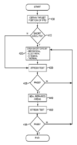
FIG. 4 is a flow diagram showing an exemplary method for repairing shorted
lines
in a target portion of a resized FPD.
DETAILED DESCRIPTION
The methods herein generally relate to resizing electronic displays, such as
LCDs or
other FPDs. Generally, such methods may involve cutting an electronic display
along
desired dimensions, resulting in a target display portion having an exposed
edge and an
excess display portion, and applying a seal along the exposed edge of the
target display
portion.
In an exemplary method, the display may be cut by onc or more of the following
steps: removing excess electronics from the display; cutting one or more
circuit boards of
the display; removing at least a portion of polarizers and/or other films, as
necessary, from
one or both plates of the display, e.g., along an intended cut line(s);
cleaning along the
intended cut line(s); and cutting or otherwise separating the display into a
target portion and
a waste or excess portion. An exemplary method for cutting the display may
include
scribing the plates along the desired line(s), e.g., with a glazer's wheel,
saw, laser, and the
like; and breaking the plates to separate the target portion from the excess
portion, thereby
creating an exposed edge along the target portion. Alternatively, the display
may be cut
using other methods, such as sawing partially or entirely through the plates,
e.g., with a
wafer saw, and the like, before or after removing polarizers and/or other
films along the
intended cut line(s).
To seal the exposed edge, the display may be stabilized, e.g., in a fixture to
apply
sufficient pressure to restore the original distance between the plates and/or
prevent the
plates from expanding. Liquid crystal (LC) may be removed from between the
plates along
the exposed edge, e.g., by wicking, draining, compressing the plates together
to eject LC
material, and the like, to create a region for sealant between the plates.
Optionally, LC
material may be injected between the plates, e.g., if excess material is
ejected from between
the plates. Adhesive or other sealant may be applied along the exposed edge,
e.g., such that
the sealant is allowed to flow, is forced, or otherwise penetrates between the
plates along the
exposed edge, e.g., without significantly changing the distance between the
plates (called
the "cell gap"). The sealant may be cured, e.g., using ultraviolet light,
heat, and the like,
81624279
thereby creating a barrier to prevent the image-generating medium from
escaping out of the
area between the plates. In addition or alternatively, one or more beads or
other layers of
adhesive or sealant may be applied externally along the out edge, e.g., for
environmental
protection and/or edge light control. Additional information on methods for
resizing
5 electronic displays may be found in US. Patent Nos. 7,535,547 and
7,780,492.
Optionally, after cutting and resettling the resized display, additional
processes may
be performed to reduce the "mullion," i.e., the inactive display area that
extends between
the active area of the resized display and the edges of the plates along the
cut and resealed
10 edge. Such reduction of the mullion, e.g., to not more than about 0.060
inch ( 1 .5 mm), may
facilitate tiling multiple displays together while minimizing the inactive
space between the
displays that may Interfere with an overall image being presented on the tiled
displays.
For example, if the cured sealant penetrates in between the plates
sufficiently to
provide a substantial seal, any external sealant may be removed, e.g., by
mechanically
grinding or scraping, chemically dissolving, and the like, In addition, if
desired, the plates
themselves may be ground or otherwise partially removed along the resealed
edge to further
the mullion created by the resized display, as long as the remaining sealant
located between
the plates provides a substantial seal to prevent leakage along the resealed
edge.
The methods herein may facilitate repair and/or prevent electrical short
circuits,
which may occur during such resizing processes at one or more locations along
the cut
and/or resealed edge of the target portion 5 of the display.
Turning to FIG. 1, a perspective view is shown of a cut edge 55 of a target
portion 5
of an LCD or other display being resized, which generally includes a pair of
substrates or
plates 20, an active image area 40, and an original seal 25 intact on the non-
cut edges of the
target portion 5. Thus, FIG. I represents the display after it has been cur as
part of a
resizing process, and before the cut edge 55 has been resealed. The edge of
the cell is
exhibited showing electrical conductor lines 30 and location of the ground
plane 35. Two
of the lines (30-s1 and 30-32, as shown in FIG. IA) arc shown shorted to the
ground plane
35. The display is not showing an image in FIG. I. If it were, the shorts
would cause a line
in the image, e.g., a black, white, or colored line, due to the inability of
the shorted line to
control the corresponding pixels connected to it. In the embodiment shown in
FIGS. I and
2, the original edge opposite the cut edge 55 (not shown for simplicity)
includes external
electronics to control the pixels and show an image on the active area of the
display. The
CA 2799026 2017-06-20
CA 02799026 2012-11-09
WO 2011/146173 PCT/US2011/031989
11
description of how the image is portrayed is not relevant to the methods
herein and is well
known to those skilled in the art.
In some cases, the cut edge 55 may be coincident with one of the conductor
lines 30
on the lower edge extending along the cut edge 55, which would further
complicate the
nature of potential shorts along the cut edge 55. For example, in such
situations, the shorts
may potentially be so extensive that a narrow sliver of the substrate panel
should be
removed. This may occur when the cut edge 55 is on top of a conductor line 30
running
parallel to the cut edge 55, e..g, between the lower and upper edges extending
from the cut
edge 55. In such situations, after the sliver is removed, the repair process
may be repeated
from the beginning.
Returning to FIG. 1, the shorted line 30-s2 is an example of a conductor line
30 that
has separated from the substrate 20 of target portion 5 sufficiently to bridge
the cell gap and
make contact with the ground plane 35. Shorted line 30-s1 is an example of a
conductor
line 30 that has separated from the waste portion of the original display in
sufficient length
to fold back and bridge the cell gap to make contact with the ground plane 35.
Shorted lines
may occur in these manners, or in other manners. These shorted lines (30-s1
and 30-s2) are
examples of the simplest form of short-circuits that may be repaired using the
methods
described herein.
As part of the resizing process described elsewhere herein, the cut edge 55 is
resealed. FIG. 2 is a plan view of the LCD in FIG. 1, after the LCD has been
resealed along
the cut edge 55 with resizing seal 45. The shorted conductor line 30-s1 is
still undesirably
present. Resizing seal 45 is shown penetrating in between the substrates 20 as
indicated by
dotted line 45a. Thus, the resizing seal 45 may include an internal portion
45a that extends
between the substrates 20 and an external portion that is attached to the end
surfaces of the
substrates 20.
The symptoms of the failed pixels associated with the shorted conductor line
30-s1
are symbolically shown as x's 50. The x's 50 represent a line of pixels or a
portion of a line
of pixels missing in an image, e.g., a test image presented on the image area
40 of the target
portion 5, emanating from the cut edge 55. The original perimeter seal 25 is
shown along
the non-cut edges for reference. In its simplest form, the image shown on the
image area 40
in FIG. 2 may be a solid color with a line or partial line 50, e.g., a black,
white, or color line
depending on the default configuration of the display, not responding to the
image
commanded. The components for generating an image are not included in FIG. 2,
but
CA 02799026 2012-11-09
WO 2011/146173 PCT/US2011/031989
12
would require electrical connections to the electrical conductors 30 shown in
the bottom of
FIG. 2 and the left edge (not shown in FIG. 2). Methods for repairing these
short circuits
will now be described in more detail.
Turning to FIG. 4, an exemplary method is shown for repairing shorted lines in
a
target portion 5 of a resized FPD. The method may be more easily performed
while the
FPD is displaying an image, so the effectiveness of the method may be seen at
each step
along the way. The method begins at step 400 by obtaining a target portion 5
of a resized
FPD. This typically occurs as part of the overall resizing process, i.e., by
separating a FPD
into a target portion 5 and a waste or excess portion (not shown), as
described elsewhere
herein. However, the source of or process for obtaining the target portion 5
is not important
to the repair method, such that this step may include simply being given the
target portion 5
which may have been created by someone else doing a resizing operation. The
target
portion 5 of the FPD at this point typically would be operational.
Once the target portion 5 is obtained, short circuits are identified at step
410.
Identification of a short circuit may be accomplished by electrically exciting
the display to
show an image on image area 40. Any shorts may result in one or more lines of
nonresponsive pixels, seen symbolically as x's 50 in FIGS. 2 and 3A. The
nonresponsive
pixels will not actually appear as x's, but rather as pixel elements in the
image display area
40 not responding correctly to the image commanded. The location of the short
may be
found by observing the intersections of the display image line of non-
responding pixels 50
and the resized cut edge 55. A failed line of pixels 50 may fade in and out as
the electrical
current heats the point of contact and burns open the short. The length of the
line of
affected pixels 50 depends, in part, of the conductivity of the short.
If a short circuit has been identified at step 410, the method proceeds to
step 420 at
which the short is repaired. Here, the repair may be accomplished by applying:
1) a
mechanical force to remove material to expose the short at a minimum or open
the short; 2)
a high voltage to the electrical conductive materials associated with the
short to fuse open
the short; 3) a chemical etchant (e.g., an acid or base) to etch away material
constituting the
short; 4) a thermal effect to burn open the short; 5) other methods to open
the short such as
re-cutting the panel to remove the portion of the panel with the short; or 6)
any combination
of the aforementioned, sequentially and/or substantially simultaneously. Each
such repair
may be performed in a manner sufficient to open the short circuit to cause the
image to be
complete and sufficiently to ensure that the short does not reoccur in any
subsequent image.
CA 02799026 2012-11-09
WO 2011/146173 PCT/US2011/031989
13
If no short circuits are identified at step 410 (or after one or more have
been
identified, and then repaired at step 420), the method proceeds to step 430 at
which
optionally the display is stress tested for further reliability, and then, if
applicable, to step
440 at which the exposed area (65) of the repaired short is resealed. Step 420
may also be
performed to a cut edge 55 that has already been resealed with a resizing seal
45, e.g., to
ruggedize the resizing seal 45, even if image defects are not exhibited
initially. For
example, the resizing seal 45 may be scrubbed with a chemical-etchant-
impregnated
material, such as a sanding block wetted with an acidic etchant, in a manner
sufficient to
remove exposed electrodes from the resizing seal, and to stress the resizing
seal 45. The
sanding block may then be used to sand the full length of the resealed edge of
the resized
display three or four times with moderate pressure. The moderate pressure is
sufficient to
remove a portion of the sealant with each stroke.
Also, the resizing seal 45 may be stress tested, and exposed electrodes
removed, by
simply rubbing the resizing seal 45 with a chemical etchant. Exposed
electrodes should be
removed because they may cause a short circuit at some later time in the FPD.
This may be
accomplished, e.g., using a cotton swab wet with the etchant agent. The seal
line may be
further stressed by rubbing it with a metal foil while displaying an image on
the display, to
see if the symptoms of a short occur. If there are exposed electrodes left on
the resizing seal
45, the metal foil may short them during contact, and thus cause pixel
failures. In that case,
further etching may be accomplished to better ruggedize the seal, and, if
necessary, the
resizing seal 45 may be replenished at the affected area. The seal line may be
further
stressed while being cleaned, e.g., using a wet tissue with alcohol and water.
Stressing the display may be accomplished in many ways, including but not
limited
to rubbing the resized edge 55 with a wet and dry cotton swab or glass rod or
wooden stick,
rubbing the resized edge with metal conductive foil, flexing the target panels
20, and/or
environmental cycling the LCD in a chamber in temperature and humidity over
the required
operating range and storage envelope. Step 440 may be applicable, for example,
if the
resizing seal 45 had already been applied to the cut edge 55 prior to arriving
at step 420, and
at step 420 the resizing seal 45 was disturbed. This situation is seen in FIG.
3B. Additional
stress testing may occur at step 450, after the resealing step at 440. The
seal may be
stressed by flexing, for example, to cause near shorts to occur, thus exposing
weak points
that may be shorted during the normal handling, usage, and/or environmental
variations to
which the display may be exposed during its operational life.
CA 02799026 2012-11-09
WO 2011/146173 PCT/US2011/031989
14
FIG. 4 shows this process occurring once for all short circuits in parallel,
but the
process may be performed on a single short at a time. During stress testing at
step 430, if
the stress testing fails (i.e., one or more shorts are identified) as
indicated by the "N" (no)
path at decision 435, the process may return back to step 420 to repair the
short(s) identified
as part of the stress testing. During stress testing at step 450, if the
stress testing fails as
indicated by the "N" path at decision 455, the process may likewise return
back to step 420
to repair the short(s) identified as part of the stress testing. Shorts
typically do not recur if
they pass a stress test. For further assurance that the short will not
reappear and cause a
pixel image failure symptom, or a new short will not appear and cause a pixel
image failure,
any resizing seal 45 removed may be replenished by applying a protective
material 60 after
removal of the short, as shown in FIG. 3C and at step 440 of FIG. 4.
As previously stated, any exposed area (65) of the resizing seal 45 exposed by
the
process may be covered to protect and prevent a recurrence of the short and
insure the
integrity of the seal 45 on the target portion 5. If the exposed area (65) is
not covered,
shorts may be induced by later disturbances such as physically rubbing the
repaired area, or
contamination with conductive materials. Further, the original display seal 25
itself may
otherwise be compromised and need to be reconstituted. Also as previously
stated,
additional (or first-time) stress testing may occur after step 440. The stress
test should
include the entire cut edge even if no symptoms of shorts are exhibited at
least once in the
process.
Before or after the resizing seal 45 is replenished with protective material
60, it may
be stress tested by rubbing the seal bead 45 with a wet cotton swab and/or a
dry cotton swab
(such as a Q-TIP swab) three or more times and a metal foil three or more
times. A
suitable wetting agent is isopropyl alcohol. A suitable metal foil is aluminum
foil. Any
marginal situation will be flexed, shorted, or made conductive by the presence
of an
applicator's wetting agent and by rubbing motion pressure to apply the agent.
The
symptoms of intermittent shorts, if any, should then occur, thus allowing them
to be
identified. The intermittent shorts may then be eliminated by the methods
described herein.
This sequence may be repeated until the intermittent shorts do not recur.
Marginal shorts
may be readdressed by the same methods and retested and re-stressed until all
symptoms of
shorts are permanently removed. The stress test may also include environmental
testing by,
for example, cycling the panel thermally and/or with humidity. Such a stress
test may be
completed if the situation warranted a high degree of confidence that shorts
would not
CA 02799026 2012-11-09
WO 2011/146173 PCT/US2011/031989
reoccur. Further, the panel may be flexed along the cut edge 55 to induce
slight motion in
the internal aspects of the seal. If intermittent shorts should occur, then
step 420 may be
repeated to achieve further separation of the shorting elements. The repair
process at step
420 will now be described in more detail.
5 At step 420, an example of mechanical force to open a short circuit is
to
mechanically remove material at the cut edge 55 in the vicinity of the short
as exhibited by
the failed line of pixels 50 in the image area 40 of the target portion 5,
shown in FIG. 2. If
the short is identified by stress testing after the resizing seal 45 is
applied, then in most
cases the failed line 50 may be fixed by simply scratching the surface of the
resizing seal
10 bead 45 with a sharp instrument. To remove more severe shorts, the
resizing seal bead 45
may be scraped away and, in the most-severe cases, the substrate 20 may need
to be
removed to reach and open the short. When removing one short, another short
may be
precipitated as exhibited by the image. The mechanical action may be repeated
until all of
the failed lines of pixels are restored if possible.
15 A specific example of a mechanical method to open a short circuit in a
target portion
5 of a resized LCD is by grinding down the resizing seal bead 45 with a high-
speed grinder
right at the point where the failed line of pixels 50 intercepts the cut edge
55 of the target
portion 5. A DREMELO tool with a cutting or grinding blade works well for this
function.
The blade may be held substantially perpendicular to the resizing seal bead 45
at the point
to be repaired. While the DREMELO tool is running at high speed, the surface
of the bead
45 may be lightly contacted. Typically, the short may be removed in an instant
with a small
penetration into the bead 45. For more difficult shorts, as shown in FIG. 1
(represented by
short 30-s2), the penetration into the bead 45 may be deeper based upon the
effect seen in
the displayed image. In difficult cases, the grinding action may penetrate
into the glass
substrate 20 before the short is extinguished and the repair may be completed.
In more
severe cases, the short may not be removed successfully using such mechanical
methods.
Further, while removing one short by such mechanical methods, another short
may occur.
To reduce the risk of recurrence, electrical, chemical, thermal, and/or other
methods
may be used alone, or in combination with each other and/or mechanical
methods, e.g., to
achieve greater assurance that a short is removed and will not return.
An example of an electrical repair method is to apply an excess electrical
voltage to
the suspect electrodes 30. Since the shorts typically have a higher
resistivity than the
conductor lines, when a current limited high voltage (a.c. or d.c.),e.g., up
to ten times the
CA 02799026 2012-11-09
WO 2011/146173
PCT/US2011/031989
16
normal voltage, is applied between the suspect lines 30 and/or between the
lines 30 and the
ground plane 35, as applicable, the shorts may open like a fuse in an
electrical circuit. The
conductive metals may turn to oxides when fused open, e.g., to instantly
become non-
conductors. In some cases, the electrical fusing process may be used without
any other
adjunct action such as the mechanical or chemical methods described herein.
An example of a chemical repair method is to apply an etching chemical such as
hydrochloric acid mixed approximately three to one with nitric acid. In some
cases, even a
small amount of citrus juice such as grapefruit juice may be sufficient. An
exemplary
method is to first open the sealant at the location of the short mechanically
and then dab the
acid along the cut edge 55 of the target portion 5 at the point of the short.
The short may
disappear with the mechanical action, but the acid etch may cause the shorting
metals to be
separated further. Since the conductive lines 30 arc typically made of thin
film metals such
as aluminum, molybdenum, and the like, the conductor lines 30 may be etched
back from
the cut substrate edge 55 to the point where they are no longer in contact
with each other or
other conductors in the immediate area. This may be done before the target
portion 5 is
resealed at step 440, since, after resealing, the chemical would have to then
penetrate the
protective material 60 if applicable, and the resizing seal 45, unless the
short extended
beyond them. The chemical may be applied by dabbing with a glass rod wetted
with the
acid or a wooden stick wetted with the acid. The acid may be washed away after
about a
minute, e.g., with a water rinse, for example, by using a cotton swab followed
with an
isopropyl alcohol cleaning. The short attended to by this series of operations
may be
completely resolved and this short is most likely ready to be repaired in step
440.
The most effective method using the chemical method is to apply it
simultaneously
while sanding the seal mechanically. As the mechanical action opens the short
or potential
short area, the chemical etches the electrodes further than may be achieved by
simple
mechanical methods. This dual action gives an increased margin of separation
of the
electrodes. Once the electrode is exposed by the mechanical action, it may be
immediately
etched away deep into the seal material that directly minimizes the degree of
mechanical
action needed. The combination of mechanical abrasion and chemical etching is
more
effective than either one alone or in sequence.
An example of a thermal repair method is to heat the local area of the short
with a
soldering iron or laser beam to thermally melt the electrodes within the
sealant and/or glass
until the short symptoms are removed. Apparatus and systems for opening
electrical lines
CA 02799026 2012-11-09
WO 2011/146173 PCT/US2011/031989
17
by a laser beam are well-known in the FPD industry. The thermal method may be
particularly useful in situations where the short is located in between the
substrates 20.
As previously mentioned, multiple forces may be applied substantially
simultaneously at step 420, such as: mechanical and electrical; mechanical and
chemical;
mechanical and thermal; mechanical, electrical and chemical; mechanical,
electrical and
thermal; mechanical, chemical and thermal; and mechanical, electrical,
chemical, and
thermal. An example of using mechanical and chemical forces substantially
simultaneously
will now be described.
At step 420, an abrasive sanding block of approximately 220 grit may be wet
with
HC1 and HNO4 (aqua regia) diluted approximately 4:1 with water. Then, the
surface of the
resized seal bead may be scrubbed three or more times with the sanding block.
Where a
short or -line-out" 50 exists, the seal edge may be scrubbed with the sanding
block using
moderate hand pressure until the line is restored. A light touch with a DREMEL
grinding
tool or razor blade may be used if necessary to remove the short. The target
portion 5 may
be set aside for a few seconds to a minute to allow time for the acid to etch
away exposed
conductors. This sequence may be used when there is no initial short to insure
that any
undesirable electrodes are removed.
Then, for the first stress test at step 430, the seal may be rubbed with
aluminum foil
to stress the seal, e.g., rubbed at least three times using moderate finger
pressure. The seal
may be cleaned with a tissue wetted with about 91% isopropyl alcohol, e.g.,
until the seal is
cleansed of any aluminum oxide and other byproducts from the acid treatment,
which may
be visually confirmed since the aluminum oxide stains the tissue black. It may
take several
rubbings using moderate finger pressure to remove the black aluminum oxide.
When the
tissue is finally clear of any discoloration after rubbing the seal, the seal
may be cleaned
again with a new clean tissue wetted with isopropyl alcohol using moderate
finger pressure.
If any shorts still appear or reappear, the process of repair (420) and stress
test (430) may be
repeated at the area of interest. If the seal is diminished from the
application of this method,
it may be replenished with protective material 60, if desired. The replenished
area of the
seal may require further stress testing and repair.
Alternatively, in a method that involves removing any external seal along the
sealed
edge and/or otherwise reducing the mullion, these processes may be repeated
one or more
times to repair any shorts and/or ensure that no shorts were created by the
mullion
reduction.
CA 02799026 2012-11-09
WO 2011/146173 PCT/US2011/031989
18
Turning now to FIG. 3, there is shown a series of details to help understand
the
methods described herein. FIG. 3A shows the conductor line 30-s1 shorted to
the ground
plane 35 as seen in FIG. 2, and within the resizing seal bead 45. FIG. 3B
shows the shorted
line 30-s1 of FIG. 3A after being opened using any of the methods described
herein. For
example, a mechanical force may have been applied to cut through the resizing
seal bead 45
and the conductor 30-s 1. Alternatively, the mechanical force may have been
used to cut
only partially through the resizing seal bead 45, or through the resizing seal
bead 45 only, or
through the resizing seal bead 45 and only partially through the conductor 30-
s1 . In these
later cases, the short may be opened after the initial mechanical force, e.g.,
by using
electrical, chemical, and/or thermal techniques, as described elsewhere
herein. FIG. 3C
shows the opened short line 30-s1 with the resizing seal bead 45 replenished
using a
protective material 60 to cover the area adjacent the repaired short circuit
30-s I . Protective
material 60 may be the same as the sealant used to seal the cut edge 55 during
the original
resizing process, or it may be another dielectric.
The criteria for success in the process is that the symptoms of a failed line
of pixels
50 in any image caused by a short at the cut edge 55 do not reappear
permanently or
intermittently (and that symptoms of no other failed line of pixels appear)
during a stress
test at the level that the display will see environmentally or mechanically
during its
operation.
While the invention is susceptible to various modifications, and alternative
forms,
specific examples thereof have been shown in the drawings and are herein
described in
detail. It should be understood, however, that the invention is not to be
limited to the
particular forms or methods disclosed, but to the contrary, the invention is
to cover all
modifications, equivalents and alternatives falling within the scope of the
appended claims.