Note: Descriptions are shown in the official language in which they were submitted.
CA 02799097 2012-11-09
WO 2011/141856 PCT/1B2011/051992
1
ADAPTIVE CIRCUIT
FIELD OF THE INVENTION
The invention describes an adaptive circuit for driving a lower-voltage
DC load from a higher-voltage AC supply. The invention also describes an LED
retrofit
lamp and a method of driving a lower-voltage DC load from a higher-voltage AC
supply.
BACKGROUND OF THE INVENTION
Advances in LED (light-emitting diode) technology have led to the
development of LEDs with a satisfactorily high light output, making them an
interesting
alternative to incandescent or fluorescent lamps. An LED lighting device can
easily be
designed to exceed an efficacy of 100 1m/W. Furthermore, LEDs are more
efficient and
more reliable than conventional lamps, and have a longer lifetime. Therefore,
using
LEDs to replace conventional lamps contributes to a reduction in energy
consumption
and reduced emissions from power plants. Packages or chips containing series-
connected LED junctions (to form an LED string with a high forward voltage)
are
suitable for low-cost general lighting applications, and LED devices directly
running
off an AC mains supply ¨ called ACLEDs or mains-compatible LEDs (MCLEDs) ¨ are
currently available. However, there are some drawbacks related to direct mains
driving.
Firstly, the current waveform given to the ACLED has a high peak value
compared to
the average value. Hence, the ACLEDs are driven with a reduced efficiency due
to
'droop'. Secondly, current flow through the ACLED package is only possible
when the
instantaneous mains voltage is higher than the forward voltage of the
package's LED
string. Therefore, during relatively 'long' periods, no light is emitted. This
is perceived
as an annoying 'flicker', so that such lamps are unacceptable for applications
such as
indoor lighting.
The flicker problem can be solved by using a rectifier and a capacitor,
however, a high voltage LED string will still be required, since the working
voltage of
the LED must match the resulting rectified mains voltage. Usually, an LED chip
CA 02799097 2012-11-09
WO 2011/141856 PCT/IB2011/051992
2
comprises one or more LED junctions connected in series such that the sum of
the
forward voltages matches the supply voltage. Evidently, the more junctions of
a given
size are connected in series to act as an LED load, the higher will be the
power
consumption of the LED load. As the skilled person knows, to obtain an LED
load with
a high forward voltage and low power consumption, a small junction size would
be
required. However, very small junctions are expensive to manufacture, and,
because of
the smaller active area, the overall efficiency obtainable by such a device is
unsatisfactory. Therefore, a low power LED package for operating off a 230 V
mains
supply cannot be realised and operated economically. To operate a more
economical,
commercially available device, for example a device rated for a 110 V mains,
additional
circuitry such as a transformer or a capacitive power supply must be used to
convert the
high input voltage to the necessary low output voltage. Such circuits are
lossy,
expensive, bulky and heavy and are associated with an unacceptably low power
factor
of less than 0.5.
However, 0.5 is the minimum power factor specified by some energy
labels for LED lamps. But even without this requirement, it is desirable to
achieve a
high power factor while minimizing losses and the cost required to achieve
such a high
power factor. One reason for desiring a higher power factor is that, at a
fixed real power
consumption and a low power factor, the input current of a load (and therefore
also the
current stress for some components) is typically high. To achieve at least the
desired
minimum power factor, the known circuits require very precise matching of the
components. However, this is made very difficult owing to the unavoidable
component
tolerances and the variations in voltages (voltage bins) even for identical
LED
packages. In an alternative approach, JP 5709736 describes the use of a
capacitive split
circuit with two or more switches for obtaining a step-down voltage. However,
in the
circuit described, at least one of the switches will be subject to extreme
voltage stress
during mains voltage transients, so that the switch may ultimately fail unless
it is
provided with additional overvoltage protection. Also, at least two switches
are
necessary, and these must be precisely synchronized to the input signal.
Therefore, it is an object of the invention to provide an improved
adaptive circuit that avoids the problems mentioned above.
CA 2799097 2017-05-03
81669261
3
SUMMARY OF THE INVENTION
According to an aspect of the invention, the adaptive circuit for driving a
lower-voltage DC load from a rectified higher-voltage AC supply comprises a
charge-storage
circuit, which charge-storage circuit comprises a first capacitor and a second
capacitor
connected essentially in series, wherein the second capacitor is connected
essentially in
parallel with the load, and an active switch realised as a controlled current
source for
controlling a load current such that, in a closed switch state, load current
is drawn at least
from the first capacitor of the charge-storage circuit, and, during an open
switch state, load
current is drawn essentially from the second capacitor.
Herein, the term 'higher-voltage' is to be understood to refer to any AC
voltage
having an essentially sinusoidal shape, for example the mains voltage
available in any
household, e.g. 230 V in Europe, 110 V in the USA, etc. In the following, for
the sake of
simplicity but without restricting the invention in any way, the AC supply may
be simply
referred to as the 'mains supply' or the 'mains'. The term lower-voltage' is
to be understood
to be a rated voltage for a device that is considerably lower than the
(relatively) higher-voltage
AC supply. For example, for a 'higher-voltage' 230 V mains supply voltage, a
'lower-
voltage' device can be a device that is in fact designed to be run off a 110 V
mains supply.
For a 'higher-voltage' 110 V mains supply, on the other hand, the 'lower-
voltage' load might
be a 60 V device.
An obvious advantage of the adaptive circuit according to the invention is
that
it allows efficient operation of a lower-voltage LED device (also referred to
in the following
as a low-power device') from a higher-voltage AC supply (for example, a 100 V
device
operated from a 230 V mains), while being a very robust circuit compared to
prior art circuits
that address this problem. Here, the term lower-voltage load' is to be
understood to mean a
DC supply voltage requiring load with a substantially lower rated voltage,
typically in the
order of only half the AC supply voltage.
Since the active switch is realised as a controlled current source, the
equalising
currents that occur between the first and second capacitor can be favourably
limited compared
CA 2799097 2017-05-03
81669261
4
to a conventional 'hard' switch. In this way, the switch is not subject to
potentially damaging
stress due to voltage and current surges when switching. Also, because only
relatively low
currents flow through the switch, it can be realised with a relatively smaller-
sized area and at
correspondingly lower cost. Furthermore, owing to the controlled manner in
which current is
supplied to the load, a relatively low value for the second capacitor is
sufficient to obtain a
low ripple on the load voltage waveform.
In contrast to existing capacitive power supply circuits, which are typically
associated with low power factors, the adaptation circuit according to the
invention can
achieve a very favourable power factor of at least 0.6.
The LED retrofit lamp according to an aspect of the invention comprises a
connecting means for connecting the lamp to a higher-voltage mains supply
signal, an LED
device rated for a lower-voltage supply, and such an adaptive circuit for
adapting a voltage of
the higher-voltage mains supply signal to drive the lower-voltage LED device.
Such a retrofit lamp can be favourably used to replace existing incandescent
lamps that are being phased out for environmental reasons, and can be driven
off a high mains
voltage such as the European 230 V mains supply. By including an adaptive
circuit according
to the invention, low-wattage incandescent lamps, for example 5 W ¨ 25 W
lamps, can be
more economically replaced by low wattage, low forward voltage LED packages
(e.g.
packages rated for 110 V mains voltage) instead of having to use LED packages
with a higher
forward voltage (and typically also higher power consumption) rated for 230 V
mains
voltage.
According to an aspect of the invention, the method of driving a lower-voltage
DC load from a rectified higher-voltage AC supply comprises the steps of
storing charge in a
charge-storage circuit, which charge-storage circuit comprises a first
capacitor and a second
capacitor connected essentially in series, wherein the second capacitor is
connected essentially
in parallel with the load; and actuating an active switch, which active switch
is realised as a
controlled current source to control a load current through the load such
that, in a closed
CA 2799097 2017-05-03
81669261
4a
switch state, load current is drawn at least from the first capacitor of the
charge-storage
circuit, and, during an open switch state, load current is drawn essentially
from the second
capacitor.
Features of the embodiment may be combined as appropriate.
CA 02799097 2012-11-09
WO 2011/141856 PCT/IB2011/051992
The adaptive circuit according to the invention can be used with any
appropriate power supply. However, since many applications for such a power
supply
adaptation may be found in the home or domestic environment, any reference to
a
rectified AC supply in the following can be understood to be a full-wave
rectified AC
5 mains supply signal, but without this restricting the invention in any
way.
The active switch can be realised using any suitable type of switch
circuitry, and can be switched according to any desired predefined condition.
In a
particularly preferred embodiment of the invention, the adaptive circuit
comprises only
a single active switch. This single switch is sufficient to implement the
switchover
between the charging and discharging states of the charge-storage circuit and
to provide
the load with a satisfactorily stable output voltage. When the active switch
is 'open',
only a minimal current (e.g. a leakage current or an auxiliary supply current
required to
drive a control input of the switch) flows through the switch in this state.
When the
active switch is 'closed', a current up to a predefined maximum value can flow
through
the switch.
The charge storage circuit is preferably realised as a 'capacitive split',
i.e.
the charge storage circuit preferably comprises two series-connected
capacitors, and the
load is connected across one of these capacitors. The input voltage to the
adaptive
circuit (and therefore also the charge-storage circuit) is applied between a
first input
voltage node and a second input voltage node, in the following also referred
to as the
'ground node'. The load is connected in parallel with the second capacitor
between an
intermediate node and the ground node. Since this type of circuit effectively
'splits' or
divides the input voltage and presents only a fraction of the input voltage
across the
load, it acts as a divider or 'splitter'.
In the actively-controlled adaptive circuit according to the invention, the
load is preferably essentially continuously driven from the second capacitor,
while the
active switch is periodically actuated to augment the load current with
current supplied
by the first capacitor as it discharges. The part of the adaptive circuit
comprising the
second capacitor connected in parallel with the load can therefore be regarded
as a type
of 'buffer' for stabilising the load voltage, while the part of the adaptive
circuit
comprising the first capacitor and the active switch can be regarded as an
additional
source of current that can be used to charge the second capacitor.
The active switch, connected essentially across the first capacitor, is
CA 02799097 2012-11-09
WO 2011/141856 PCT/IB2011/051992
6
preferably realised to decouple the load from the first capacitor (and
therefore also from
the input supply) during a charge-storage circuit charging state, i.e. while
the first and
second capacitors are charging (when the momentary voltage across the input to
the
adaptive circuit is high enough to charge the series connection of the two
capacitors)
and to supply the load with current from the second capacitor during a
discharging state
of the charge-storage circuit (when the voltage across the input to the
adaptive circuit
has decreased). In this way, the active switch can control or limit the
current flowing
through the load, and can ensure a sufficient supply of current to the load
regardless of
the charging status of the capacitive-split circuit.
An active switch can be realised using any suitable electronic
components. In a preferred embodiment of the invention, the active switch
comprises a
transistor such as a bipolar junction transistor (BJT), a field-effect
transistor such as a
MOSFET, a Darlington pair, etc., in conjunction with a voltage source
connected
between the intermediate node and a control input (e.g. base or gate) of the
transistor.
Preferably, a resistor is included in the path shared by the transistor load
current and the
load drive signal. Effectively, the control input voltage minus the voltage
drop across
the transistor (the base-emitter voltage or the gate-source voltage)
determines the
maximum possible voltage drop across this resistor and therefore also the
maximum
possible current through the active switch. The voltage source can be any
suitable
component or circuit that is capable of presenting an essentially constant
voltage
regardless of the current flowing through it. Various possibilities will be
known to the
skilled person. For example, the voltage source could comprise a Zener diode.
In such
realisations, where the closing of the switch depends on a voltage (the base
or gate
voltage), the active switch behaves as a dependent or controlled current
source.
The active switch is opened or closed according to the voltage at the base
or gate of the transistor. By controlling this voltage, the instant at which
the transistor
opens or closes can also be controlled. Therefore, in a particularly preferred
embodiment of the invention, the active switch also comprises a switch
controller
realised to close the active switch in a specific input voltage range. In such
a realisation,
for example, the switch controller can comprise a transistor whose base or
gate voltage
is controlled by a Zener diode with a suitable knee voltage connected between
the gate
and an output of a voltage divider connected across the input voltage nodes.
Whenever
the input voltage rises above a certain voltage level, the Zener diode breaks
down, the
CA 02799097 2012-11-09
WO 2011/141856 PCT/IB2011/051992
7
switch controller transistor starts conducting, and hence lowers the voltage
at the
control input of the active switch, and the active switch is opened, i.e.
allowing hardly
any current to flow from the first capacitor to the parallel connection of the
LED and
the second capacitor.
In a further preferred embodiment of the invention, the switch controller
could be realised to close the active switch at a specific time. In such a
realisation, the
switch controller could comprise a micro-controller programmed to supply a
suitable
switch actuating signal according to a predefined switching scheme. A lamp
comprising
such a switch controller could then be exactly 'tuned' so that its active
switch is opened
or closed only at certain predefined instants relative to the input voltage
shape.
Typically, the switching scheme in such a timed embodiment will be
synchronised to
the AC input voltage. Combined voltage- and time-controlled switching is also
possible. As an example, the active switch could be closed some time after the
mains
voltage has dropped below a certain first threshold value and be opened as
soon as the
mains voltage rises above a (possibly different) second threshold value. The
controlling
circuitry for the active switch is preferably adapted to the voltage and the
frequency of
the AC input signal, i.e. different threshold values and different timings may
be used for
systems with different characteristics e.g. a mains frequency of 50 Hz or 60
Hz; a mains
supply voltage of 100 V or 230 V, etc.
As indicated above, the adaptive circuit uses a higher-voltage rectified
AC signal to produce a lower-voltage output for driving a load. The adaptive
circuit can
therefore be used in conjunction with any suitable rectification circuitry,
and can be
realised with the appropriate connection means, and can be driven from any
suitable
AC signal. Therefore, in a particularly preferred embodiment of the invention,
the
adaptive circuit includes such a rectification means, which could, for
example,
comprise a diode bridge rectifier for performing a full-wave rectification on
the AC
signal, for example from an AC mains supply. To improve the behavior of the
circuit in
response to transients, the adaptive circuit can also comprise an inrush
resistor for
damping a voltage or current surge.
The components of the adaptive circuit are preferably chosen so that the
adaptive circuit is particularly suited for adapting an input voltage from a
230 V mains
supply to an output voltage with a range of 80V to 140V.
When realised for mains supply operation, such as European mains
CA 02799097 2012-11-09
WO 2011/141856 PCT/IB2011/051992
8
supply, the low-power LED device of the LED retrofit lamp according to the
invention
preferably comprises a 2W LED device and the adaptive circuit is realised to
drive the
LED device from a 230 V mains supply by a suitable choice of components as
indicated
above. Of course, any other suitable LED package could be used in the
inventive LED
retrofit lamp, and the embodiment mentioned here is to be understood to be
exemplary.
The active switch can be opened or closed at any time. However, since
the charging and discharging behavior of the capacitors is directly related to
the mains
voltage shape, the shapes of the voltages at the first input voltage node and
the
intermediate node are also linked to the mains voltage shape. The load can
therefore be
optimally driven by closing or opening the switch at appropriate instants in
time.
Therefore, in a preferred embodiment of the method according to the invention,
the
active switch is actuated synchronously to the voltage of the AC mains supply,
i.e. the
switch is opened or closed at instants that correspond to certain 'points'
along the input
voltage shape.
The actual instant at which the active switch is opened or closed can
influence the circuit in a number of ways. As long as the switch is open,
input current
can only be drawn from the mains while the capacitors are charging. In the
method
according to the invention, by closing the switch at a certain stage, i.e. by
influencing
the behavior of the charge-storage circuit, an additional 'path' can be
offered for input
current flow. Therefore, in a further preferred embodiment of the method
according to
the invention, the instant of actuation of the active switch is chosen
according to a
desired apparent reactance of the adaptive circuit, i.e. the reactance 'seen'
from the input
terminals. By switching the active switch closed during a certain 'section' of
the input
voltage shape, the load can be seen - from the point of view of the mains
supply - to
behave as a capacitive load or an inductive load. In this way, the lamp can be
'tuned' to
act as a capacitive or inductive load. For a lighting application with many
such retrofit
LED lamps, a certain proportion can be realised to act as inductive loads, and
another
proportion can be realised to act as capacitive loads. In this way, the
overall reactance
of the loads is neither excessively capacitive nor excessively inductive.
Another
advantage of controlling the current flow relative to the charging peak of the
charge-
storage circuit is that the harmonics of the input current waveform can be
influenced.
Generally, it is desirable to reduce the number of higher-order harmonics in
the current
drawn from the mains, since higher-order harmonics detract from the overall
power
CA 02799097 2012-11-09
WO 2011/141856
PCT/IB2011/051992
9
factor of the circuit. By using a favourably chosen switching scheme, the
input current
can be adjusted so as to have a marked fundamental and only minor higher-order
harmonics. The adaptive circuit can also be realised to comply with further
regulation
requirements for lighting applications. For some countries, not only power
factor and
harmonics are regulated, but the starting point, the peak point and the ending
point of
input current flow from the mains into the load are also specified. When these
parameters are specified, there are usually less stringent requirements placed
on the
higher-order harmonics. The adaptive circuit can be realised to provide the
required
input current wave shapes in order to fulfil such requirements, for example by
making
more use of the continuous controllability over time of the active switch. In
most of the
examples described so far, the discharging of the first capacitor via the
active switch
was performed while the input voltage is lower than the voltage stored in the
capacitor.
In these cases, the discharge current is not noticeable on the input supply
terminals of
the adaptive circuit. When activating (i.e. closing the switch) takes place
during a time
period where the instantaneous value of the input voltage is lower than the
voltage
stored in the capacitor, part of the switch current is directly drawn from the
input
terminals.
Hence, during these periods, an actively controlled input current can be
programmed.
In a simple example, a predefined current waveform with optimized
efficiency and harmonic content can be previously determined and stored in a
memory
of the adaptive circuit. Then, after synchronization to the input frequency,
the active
switch current is controlled according to the predetermined waveform to
generate the
desired input current. To this end, the adaptive circuit can comprise a non-
volatile
memory and a waveform playback unit. Preferably, the adaptive circuit
comprises a
microcontroller capable of running an appropriate programme or algorithm.
In a preferred embodiment of the invention, the total amount of power
delivered to the load is determined by the control signal given to the active
switch. By
appropriate timing of the switch relative to the signals on the input side,
the current
delivered to the load, and therefore also the power, can be controlled as
desired.
Since it is desirable to allow the capacitors to fully charge up before
allowing them to discharge again, in a further preferred embodiment of the
invention,
the active switch is switched from open to closed to initiate a discharging
state of the
CA 02799097 2012-11-09
WO 2011/141856 PCT/IB2011/051992
charge-storage circuit. In other words, the switch is only closed after the
input voltage
has peaked, since, after this time, the charge across the capacitors has
reached its
maximum and will not increase any further.
When the active switch is realised using a transistor, the switch will be
5 closed, i.e. conducting, whenever the base or gate voltage exceeds a
certain level, and
the switch is effectively controlled with a discrete drive signal that can be
generated
using an appropriate Zener diode. The active switch could however be realised
using an
alternative to the discrete Zener voltage source described above. Therefore,
in another
preferred embodiment of the invention, the active switch is actuated by a
continuous
10 drive signal. For example, with suitable circuitry between a transistor
for measuring the
supply voltage and the active switch control input, the active switch current
can be
decreased and increased slowly, such that the active switch receives a
continuous drive
signal for at least part of the time. In a further embodiment, the
microcontroller can
generate such a continuous drive signal (e.g. using a timer based pulse-width-
modulation generator and a low pass filter, or using a digital-to-analogue
converter) and
can be realised to not only control the active switch to be open or closed,
but also to
actively control the permitted amount of current at any point in time.
BRIEF DESCRIPTION OF THE DRAWINGS
Fig 1 shows a prior art adaptive circuit;
Fig. 2 shows a circuit diagram of an adaptive circuit according to a first
embodiment of the invention;
Fig. 3 illustrates the principle of operation of the circuit of Fig. 2;
Fig. 4 shows a circuit diagram of an adaptive circuit according to a
second embodiment of the invention;
Fig. 5 shows graphs of current and voltage for the adaptive circuit of Fig.
4;
Fig. 6 shows a further set of graphs of current and voltage for the
adaptive circuit of Fig. 4;
Fig. 7 shows a schematic rendering of a retrofit LED lamp according to
an embodiment of the invention.
CA 02799097 2012-11-09
WO 2011/141856 PCT/IB2011/051992
11
In the drawings, like numbers refer to like objects throughout. Objects in
the diagrams are not necessarily drawn to scale.
CA 02799097 2012-11-09
WO 2011/141856 PCT/IB2011/051992
12
DETAILED DESCRIPTION OF THE EMBODIMENTS
Fig 1 shows a prior art adaptive circuit 10 of the type described in
JP 5709736 for stepping down an input voltage applied across input
terminals 170, 171 in order to obtain a lower voltage for a load connected
across output
terminals 180, 181. This type of circuit is suited for small device
applications such as
hand-held devices, where a transformer would be unsuitable owing to its size
and
weight. The input voltage can be a DC voltage or a rectified AC voltage. A
first switch
11, a first capacitor 13, a diode 16 and a second capacitor 14 are connected
in series. A
second diode 15 is connected in parallel with the first diode 16 and the
second capacitor
14. A second switch 12 is connected across the first capacitor 13 and first
diode 16. To
step down the input voltage, the first and second switches 11, 12 are switched
alternately. When the first switch 11 is closed (and the second switch 12 is
open), the
series-connected capacitors 13, 14 are charged and the load is driven by the
voltage
accumulating between the first diode 16 and the second capacitor 14. Then, the
second
switch 12 is closed and the first switch 11 is opened. During this time, the
capacitors 13,
14 discharge so that the load is driven by both capacitors 13, 14. In this
prior art circuit,
the values of the capacitors 13, 14 should be equal to obtain an output
voltage that is
half the input voltage. By extending the step-down circuit to comprise N
capacitors in
series, 1/N voltage division can be obtained.
However, this type of circuit 10 has a number of disadvantages. For
example, if this circuit is driven off the mains, both switches must be
exactly
synchronised in a specific temporal relationship to the mains voltage signal.
A
minimum of two switches is required in order to be able to use a full-wave
mains input.
Also, since the current flow between the two capacitors at the instant of
closing the
switch 12 can reach a large value, the components must be rated for a high
peak stress,
necessarily causing them to be larger and more expensive compared to
components that
are not required to withstand such peak currents. Furthermore, while the
switch 11 is
opened, any voltage transients present on the input terminals 170, 171 (e.g.
originating
from voltage surges on the mains to which the input terminals are connected)
are not
limited or clamped and will result in a voltage stress across switch 11. In a
closed state
of switch 11, surges will lead to a high current through switch 11. In brief,
switch 11 is
exposed to high stress when operated from a real mains voltage distorted by
surges.
Furthermore, only fixed 1/N voltage division ratios are possible, so that the
applications
CA 02799097 2012-11-09
WO 2011/141856 PCT/IB2011/051992
13
are limited.
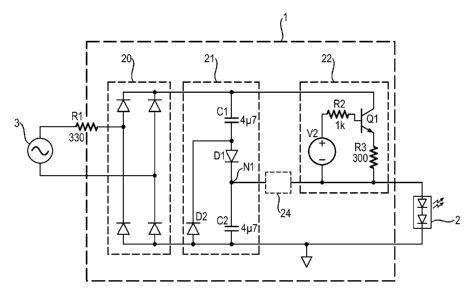
Fig. 2 shows an adaptive circuit 1 according to a first embodiment of the
invention, used to drive a lower-voltage load 2 from a higher-voltage input.
In this
example, the higher-voltage input is derived by performing full-wave
rectification on a
230 V AC mains supply 3, using a diode bridge rectifier 20. A resistor R1 may
precede
the rectifier 20. The load to be driven by the adaptive circuit 1 comprises a
2W 110 V
LED package 2. The adaptive circuit 1 comprises a charge-storage circuit 21
composed
of a first capacitor Cl and a second capacitor C2 connected in series, with
two diodes
D1, D2, in an arrangement 21 which can be referred to as a 'modified valley-
fill circuit'.
The adaptive circuit 1 also comprises an active switch 22 acting as a
controlled current
source 22, which is constructed using a voltage source V2, a transistor Ql,
and current-
limiting resistors R2, R3. Example values for the circuit components are given
in the
diagram.
An additional optional resistive circuit element 24 can be inserted in the
path between the active switch 22 and the second capacitor C2 in order to
limit the
current flowing through this path at any one time. The effective value of such
a resistive
circuit element 24 may be dependent on the direction in which current flows
through it.
To this end, this resistive circuit element 24 can be realised by a suitable
arrangement of
resistors and/or diodes.
Fig. 3 illustrates the three-state principle of operation of this circuit 1.
The diode bridge 20 supplies a full-wave rectified signal essentially
comprising a series
of positive sine-wave halves. In the upper part of the diagram, in a 'charging
state' S-I,
the switch 22 is opened while the capacitors Cl, C2 charge from the rising
input voltage
signal. Since the switch 22 is open, this part of the circuit can be ignored,
as indicated
by the dotted lines. During this time, the load 2 is fed only by the second
capacitor C2
while it is charging. For the sake of clarity, in Fig. 3, only the relevant
components in
each state are denoted by their reference signs.
Once the capacitors Cl, C2 have charged, no current is drawn from the
mains 3. Therefore, in the subsequent 'transition state' S-IT, the supply side
of the circuit
can be ignored, as indicated by the dotted lines in the second part of the
diagram. The
switch is still open, so that this can also be ignored, as indicated by the
dotted lines. The
load 2 is again driven only from the second capacitor C2.
As the input voltage drops even further, both capacitors Cl, C2 can
CA 02799097 2012-11-09
WO 2011/141856 PCT/IB2011/051992
14
discharge again, as shown in a third state S-111 in the lower part of the
diagram. The
switch 22 is closed, so that current flows through the transistor Ql. In this
'discharging
state' or 'balance state' S-ITT, the load 2 is supplied with current mainly by
the
discharging first capacitor Cl. In this state, the load 2 may also draw
current from the
second capacitor C2, as indicated in the diagram. Equally, the second
capacitor C2 may
be charged again by a current diverted from the active switch 22. The actual
current
distribution through these circuit elements will depend largely on the
voltages at the
various nodes at any one instant. Since the input voltage is dropping, no
current is
drawn by the capacitors Cl, C2 from the supply side of the circuit, so that
this can be
ignored, as indicated by the dotted lines.
The voltage applied to the load 2 during these three states, S-I, S-II, 5-111,
cannot exceed the voltage at node Ni, which is effectively limited to a
maximum of half
the input peak voltage, thus ensuring that the lower-voltage load 2 can be
driven safely.
The highest voltage that can be accumulated across the second capacitor C2 is
governed
by the choice of components for the first and second capacitors, and whether
these are
matched or not.
Fig. 4 shows a realisation of the adaptive circuit l' according to a further
embodiment. Again, the adaptive circuit l' comprises a diode bridge rectifier
20 that
performs full-wave rectification on a mains input voltage from a mains supply
3. A
charge-storage circuit 21' comprises a pair of series-connected capacitors Cl,
C2 and
two diodes DI, D2. The load 2 is connected across the second capacitor C2. In
this
realisation, the active switch 22' comprises a Darlington pair Q I, Q2 whose
base signal
is delivered via the resistor R2, the base voltage being limited by a first
Zener diode Zl.
The voltage across the first Zener diode Z1 is in turn governed by a switch
controller
220, which comprises a voltage divider R4, R5, a second Zener diode Z2, and a
transistor Q3. In Fig 4, the components R4, R5, Z2, R6, Q3, Z1 in conjunction
with the
resistor R2 depict a possible embodiment of the voltage source V2 described in
Figs. 2
and 3. A decoupling diode D3 is included to permit the input voltage to be
measured
accurately by the switch controller 220.
While the switch 22' and the switch controller 220 are shown to be
separate parts of the overall circuit in this diagram, it will be clear to the
skilled person
that the switch 22 and the switch controller 220 operate in conjunction with
one another
and can therefore be regarded as a single 'entity' or single active switch.
CA 02799097 2012-11-09
WO 2011/141856 PCT/IB2011/051992
Again, component values are indicated in the diagram. The first and
second Zener diodes Z1, Z2 can have a Zener voltage of 10V, the transistors
Ql, Q2 are
preferably rated for voltages of more than half the peak input voltage, while
the
transistor Q3 can be a low-voltage transistor type, e.g. BC337. In this
embodiment,
5 whenever the voltage at the output of the voltage divider R4, R5 reaches
the Zener
voltage of the second Zener diode Z2, the transistor Q3 becomes conductive, in
turn
diverting the current delivered via resistor R2, thus shutting down base
current into the
Darlington pair Ql, Q2, such that the active switch 22' is effectively opened.
In the case
that the momentary value of the input voltage is too low to activate Q3, the
transistor
10 pair Ql, Q2 receives base current via R2 and allows a current flow
according to the
value pre-programmed by the Zener diode Z1, the emitter resistance R3 and the
effective base-emitter voltage of the Darlington pair Ql, Q2. In the example
given here,
the allowed current will be approximately the difference between the Zener
diode
voltage and the base-emitter voltage of the Darlington pair, divided by the
emitter
15 resistance R3. Using the components shown, this gives a current of about
(10 V ¨ 1.4 V)
/ 300 = 28.6 mA.
For this adaptive circuit l', using the components indicated, the input
power is 2.72 W, while the LED power is 2.12 W, so that the efficiency of the
circuit
equals 78%. The power factor of this adaptive circuit l' was measured to be
0.61, which
favourably exceeds the minimum of 0.5. The amount of optical flicker in the
light
emitted by the LED load 2 was analysed, and a flicker index of 0.14 was
determined.
Since most of the optical flicker for this circuit is at 200 Hz, it
effectively cannot be
perceived by the human eye, making the adaptive circuit l' particularly
suitable for use
in a retrofit lamp application. An optional capacitive ballast CB is shown,
which can be
used to provide a further match between the AC input voltage and the LED load
voltage
and maintain a higher efficiency even for LED load voltages that are not
matched to
approximately half the AC input voltage. This in turn can improve the
efficiency even
more, while leaving the favourably high power factor nearly unchanged, so that
an
efficiency of 87% can be achieved with a power factor of 0.6. The circuit can
be
modified according to the requirements. For example, instead of using a
bipolar
Darlington transistor or a pair of transistors Ql, Q2 in Darlington
configuration, a FET
could be used.
Fig. 5 shows a series of graphs for current through certain elements of the
CA 02799097 2012-11-09
WO 2011/141856 PCT/IB2011/051992
16
circuit of Fig. 4. Supply current lp, is drawn from the AC source 3 as long as
the
capacitors Cl, C2 of the charge-storage circuit 21' are charging. The load
current 'load
through the load 2 is shown to fluctuate between approximately 20 mA and 34
mA. The
first capacitor current Ici through the capacitor Cl increases rapidly to a
peak during
charging and then drops off to zero again when the capacitor Cl is fully
charged. As
long as the switch remains open, no current flows through the fully charged
first
capacitor Cl. Then, when the active switch 22' is closed, there is a negative,
discharging
current in the first capacitor current 'Cl, which level is controlled by the
active switch.
When the switch is opened, the first capacitor current 'Cl drops back to zero.
The switch
current 1,, through the Darlington pair Ql, Q2 toggles between 0 A (active
switch is
open, corresponding to states S-I and S-II in Fig. 3) and -44 mA (active
switch is closed
and conducting, corresponding to state S-III in Fig. 3).
The second capacitor current 1C2 drawn from the second capacitor C2 is a
composition of the input current charging peak, the LED load drive current and
the
current delivered via the active switch. In this embodiment, the current
delivered from
the first capacitor Cl through the active switch 22' is higher than the actual
current
consumption of the LED load 2, hence part of the current flows as a charging
current
into the second capacitor C2. The second capacitor current 1c2 reaches a
maximum in
the region of 40 mA during the charging state of the charge-storage circuit
21', whereas
the peak charging current in the first capacitor Cl is approximately 70mA. The
difference between these currents is the current 'load supplied to the LED
load 2. Since
the load 2 is placed essentially in parallel with the second capacitor C2, the
load 2 is
continuously driven.
At the bottom of the diagram, voltages Uci, Uc2 are shown for the first
and second capacitor Cl, C2, respectively. The first capacitor voltage lic1
can reach
about half of the peak input voltage, while the voltage Uc2 across the second
capacitor
C2 (and therefore also the voltage across the load 2) oscillates about 120 V.
This
voltage level depends of course on the forward voltage of the lower-voltage
LED load
2.
Fig. 6 shows another set of graphs for the mains voltage Ups, mains
current Ips, first capacitor voltage Ucl and load voltage Uc2. This graph more
clearly
shows the relationship between the mains voltage Ups and the load voltage Uc2,
and that
the load voltage oscillates as the load 2 is fed by the second capacitor C2
while charging
CA 02799097 2012-11-09
WO 2011/141856 PCT/IB2011/051992
17
and then as the load 2 draws from the charged second capacitor C2 (while the
active
switch is open), and then as the load is fed by both capacitors Cl, C2 (while
the active
22' switch is closed). Most importantly, Fig. 6 shows that the actuation of
the active
switch does not result in artefacts on the mains input side of the adaptive
circuit. The
active switch is closed in a period where the mains voltage is so low that
hardly any
current flow is possible from the mains into the adaptive circuit. Therefore,
only a very
small current spike 60 appears on the mains side at the instant when the
switch is
closed. With appropriate adjustments, even this small spike 60 can be
suppressed. For
example, the activation period of the active switch could be shortened to
suppress the
spike 60. Also, the activation period of the active switch could be shifted
towards an
earlier instant, which would also result in the small spike 60 being
suppressed.
In an alternative embodiment, as already indicated above, the activation
period of the active switch could be prolonged or moved towards an earlier or
a later
part of the mains period to intentionally draw additional current from the
mains and thus
actively influence the apparent capacitive or inductive behavior of the
adaptive circuit
as seen from the input terminal.
Fig. 7 shows a retrofit LED lamp 4 according to the invention, realised as
a 'candle' with a suitable connector 40 for screwing the lamp into a
corresponding
socket to replace an incandescent lamp of the same type. In place of a
filament, this
retrofit lamp comprises a DCLED or ACLED package 2, rated for a lower-voltage
supply such as a 110 V mains, and an adaptive circuit 1, l' of the type
described above
for adapting the higher-voltage mains supply signal to a lower voltage
suitable for
driving the LED package 2.
Although the present invention has been disclosed in the form of
preferred embodiments and variations thereon, it will be understood that
numerous
additional modifications and variations could be made thereto without
departing from
the scope of the invention. The trade-off between losses in the active switch,
high-
frequency switching artefacts and low-frequency harmonics of the input
waveform to
the load can be adjusted as desired. For example, by controlling the active
switch with a
continuous drive signal that is variable in amplitude, high frequency
artefacts can be
avoided. Other fine-tuning steps which will be known to the skilled person can
be taken
to improve the circuit behavior according to the application for which the
adaptive
circuit is intended.
CA 02799097 2012-11-09
WO 2011/141856
PCT/IB2011/051992
18
For the sake of clarity, it is to be understood that the use of "a" or "an"
throughout this application does not exclude a plurality, and "comprising"
does not
exclude other steps or elements. A "unit" can comprise a plurality of units
unless
otherwise stated.