Note: Descriptions are shown in the official language in which they were submitted.
CA 02799560 2012-11-15
WO 2011/144735 PCT/EP2011/058253
-1-
"Compacted patch antenna"
DESCRIPTION
The present invention relates to a compacted patch antenna.
Patch antennas, also known as rectangular micro-strip antennas, are
known in the state of the art. They consist of a single metal patch suspended
over a ground plane and a dielectric substrate arranged between the ground
plane and the metal patch; the antenna assembly is generally contained in a
plastic cover which protects the antenna against possible damages. They are
used in various applications as they have a compact and light structure, a
low profile, a geometry conformable to the surfaces and finally are easily
interfaceable with the signal supply network (which may comprise
amplifiers, filters and/or power dividers). Disadvantages include medium-
low efficiency (due to low-cost materials), an intrinsically narrow operating
band (due to the resonant-type operation) and the non-remote possibility of
exciting surface waves in the substrate, which are sources of spurious
radiation. The operation of the patch antenna is of resonant type and the
resonance frequency mainly depends on shape and size of the printed region
and on the dielectric constant of the substrate. Instead, the input impedance
depends on the supply point, whereby a mode should be selected for
supplying the antenna which takes the signal close to the point
corresponding to the desired impedance.
The metal patch has a length equal to half the wavelength if the
antenna is used in radiofrequency. The micro-strip antennas have various
advantages as compared to conventional microwave antennas, since they
may easily cover a wide range of frequencies, typically from 100 MHz to
100 GHz. Said antennas have a low weight, a small volume, a high
mechanical sturdiness and a low production cost, However, they have
certain disadvantages related to the narrow band and to the quite low gain,
about six decibels; the band may be increased by using high-permittivity
dielectric layers and the gain may be increased with micro-strip antenna
CA 02799560 2012-11-15
WO 2011/144735 PCT/EP2011/058253
-2-
arrays.
Radiation phenomena of a micro-strip line are known to be
significantly reduced if the substrate employed is thin and has a high
permittivity. For these reasons, low-permittivity thick substrates are
preferred when micro-strip antennas with high irradiation efficiency are to
be provided.
The length of the patch strongly determines the resonant frequency
and is a critical parameter in determining the band; indeed, typically a
micro-strip antenna has a much smaller bandwidth as compared to that of a
normal resonant antenna. The increased height of the substrate and a smaller
dielectric constant may increase the bandwidth, but this could lead to
geometrical parameters which are incompatible with the integration scale
chosen. To a first approximation, the resonant frequency is inversely
proportional both to the length and to the square root of the relative
permittivity of the dielectric. Since width and length for a real patch have a
finite measure, the fields at the edges are subject to fringing effect. This
effect is due to the field lines being required to pass through a non-
homogeneous medium consisting of two separate dielectrics: substrate and
air.
There are other patch antennas which are highly used in wireless
transmissions, having a length equal to 1/4 of the wavelength and having the
radiating metal patch short-circuited to the ground plane, such as PIFA
antennas (Planar Inverted F-Antennas).
In view of the state of the art, it is the object of the present invention to
provide a compacted patch antenna which is different from the known
antennas. The antenna in accordance with the invention has small
dimensions and preferably a high selectivity of the bandwidth at the resonant
frequency.
In accordance with the present invention, said object is achieved by a
compacted patch antenna, in particular to be installed in a motor vehicle,
comprising an electrically supplied strip radiating element, a ground plane to
CA 02799560 2012-11-15
WO 2011/144735 PCT/EP2011/058253
-3-
which said strip radiating element is connected at a first end by means of
metal link, and at a second end opposite to the first end, by means of a
variable capacitor, a printed circuit the bottom surface of which is integral
with the ground plane, a dielectric material layer arranged between the strip
radiating element and the printed circuit, said strip radiating element being
substantially parallel to said ground plane, characterized in that said
dielectric material layer has a relative dielectric constant ranging from 3 to
6
and a loss factor ranging from 0.03 to 0.1.
The features and advantages of the present invention will become
apparent from the following detailed description of a practical embodiment
thereof, shown by way of non-limiting example in the accompanying
drawings, in which:
figure 1 is a top view of the compacted patch antenna in accordance
with an embodiment of the present invention;
figure 2 is a diagrammatic, cross-section view of the antenna in figure
1;
figures 3 and 4 show diagrams of the gain of the antenna in figure 1
according to the frequency;
figure 5 shows a diagrammatic, cross-section view of the compacted
patch antenna in accordance with a variant of the embodiment of the present
invention;
figure 6 is a top view of the compacted patch antenna in figure 5;
figure 7 shows a diagram of the gain of the antenna in figure 5
according to the frequency;
figure 8 shows a motor vehicle in which the compacted patch antenna
in figure 1 or figure 5 has been installed;
figure 9 shows the compacted patch antenna in figure 1 or figure 5 in
greater detail, fixed to the motor vehicle.
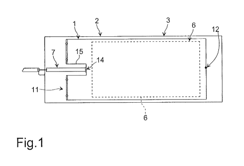
With reference to figures 1 and 2, a compacted patch antenna is shown
in accordance with an embodiment of the present invention. The antenna
comprises a strip radiating metal element or micro-strip I preferably having
CA 02799560 2012-11-15
WO 2011/144735 PCT/EP2011/058253
-4-
a length equal to 1/4 of the wavelength of the resonant frequency, e.g. of the
frequency Fo=434 MHz. Said strip metal element 1 is connected to ground
GND at one end 11, and at the opposite end 12 is connected to a variable
capacitor 5 connected to ground; said variable capacitor 5 is adjusted to tune
the resonant circuit of the antenna to the resonance on the operating
frequency.
The antenna comprises a flat base 2 with a printed circuit, the
completely coppered bottom face of which is the ground plane 3; the strip
metal element 1 is parallel to the ground plane 3. The height h of the antenna
with respect to the ground plane is about 7 mm; the space between the strip
metal element 1 and the ground plane 3 is partially filled with the material
of
the printed circuit and partially with dielectric material 6 with suitable
dielectric constant and suitable loss factor. The dielectric material 6, in
particular plastics, is glued to the strip radiating element 1 and to the flat
base 2 with printed circuit, thus obtaining a rigid, firm planar structure
even
in the presence of detectable, strong mechanical vibrations, for example if
the antenna is installed in a car.
The antenna comprises a small micro-strip 7 integral with the strip
metal element I and adapted to supply the antenna; the impedance matching
is also performed through micro-strip 7, In particular, the strip metal
element
1 comprises a small rectangular split 15 on the side of end 11 which
continues towards end 12. Split end 14 is the contact point between micro-
strip 7 and metal element 1.
The geometry of the compacted patch antenna in accordance with the
invention is of rectangular type, but so that metal element 1 is larger than
dielectric layer 6 and smaller than printed circuit 2 with ground plane 3.
The dielectric material layer 6 has a relative dielectric constant sr
ranging between 3 to 6 which allows the size of the patch antenna to be
reduced; indeed, a metal strip element may be used, having a length equal to
1/4 of the wavelength, while the thickness of the antenna is less than one
centimetre.
CA 02799560 2012-11-15
WO 2011/144735 PCT/EP2011/058253
-5-
Moreover, the dielectric material layer 6 has a loss factor tan&_ ranging
from 0.03 to 0.1, preferably from 0.05 to 0.1, which allows the bandwidth to
be increased to the resonant frequency of the antenna, i.e. allows the
bandwidth to be tuned to the resonant frequency thereof without invalidating
the proper operation of the antenna. Indeed, with a dielectric material with a
loss factor tan8E less than 0.03 (e.g, 0.01), a very critical antenna would be
obtained, which would be difficult to manufacture and calibrate, and which
could lose its resonant frequency over the life of the antenna. There is no
need - especially in the field of motor vehicle or automotive applications --
for the bandwidth about the resonant frequency to be narrow in order not to
invalidate the proper operation of the antenna over the years; an antenna
with a very narrow bandwidth would be critical and the resonant frequency
thereof could significantly vary due to the mechanical and thermal stresses
found on motor vehicles, for example. In particular, the choice of a loss
factor tan6 of the dielectric material ranging between 0.05 to 0.1 allows a
good balance between the need for an antenna with a bandwidth such as to
decrease undesired disturbances and signals on the one hand, and the need
for an antenna which is easy to manufacture and calibrate, and especially
which has a long life, on the other hand. For example, certain dielectric
materials which may be used to fill the space between metal element 1 and
ground plane 3 are FR4 material (Glass Reinforced Epoxy) with dielectric
constant 4.7 and loss factor 0.03, and especially PMMA material (Poly
Methyl Metacrylate) with dielectric constant 3.7 and loss factor 0,06, or
ABS material (Acrylonitrile Butadiene Styrene) with dielectric constant 3.5
and loss factor 0.09.
The antenna exhibits a resonance tuned to a frequency ranging
between 300 megahertz to 1 gigahertz and the dielectric material allows the
bandwidth to be tuned to match it to the various application needs. However,
there is a need for the bandwidth to be at least equal to or greater than 15
MHz.
Figure 3 shows the anti-gain diagrams of AG antenna and VSWR
CA 02799560 2012-11-15
WO 2011/144735 PCT/EP2011/058253
-6-
(Voltage Standing Wave Ratio), i.e. a parameter which denotes, in decibels,
the ratio between the maximum and minimum voltage values of a stationary
wave pattern according to the frequency if the dielectric is the PMMA
material; the bandwidth centred on the resonant frequency Fo=434 MHz is
15 MHz with a gain of some decibels.
Figure 4 shows the anti-gain diagrams of AG antenna and VSWR, in
decibels, according to the frequency if the dielectric is the ABS material;
the
bandwidth centred on the resonant frequency Fo=434 MHz is 25 MHz with
a gain of some decibels but less than the gain of the antenna in figure 3.
A compacted patch antenna in accordance with a variant of the
embodiment of the present invention is shown in figures 5 and 6. Said
antenna differs from the antenna in figures 1 and 2 due to the presence of a
SAW filter 20 with the corresponding impedance matching circuit 21,
coupled with the small micro-strip 7 which allows the antenna to be
supplied.
The SAW filter 20 allows the antenna selectivity to be increased, in
particular if the antenna is used in a car while keeping the features of
mechanical stability and high reliability of the antenna, as shown in the anti-
gain diagram of the AG antenna in figure 7 with bandwidth centred on the
resonant frequency Fo-434 MHz.
The antenna in accordance with the present invention is adapted to be
used in data transmitting and receiving systems for vehicles, preferably for
motor vehicles. The antenna is first arranged within an airtight, plastic
cover
200 which is fixed to the frame 201 of a motor vehicle 202, preferably to the
outer surface of the bottom of frame 201 of motor vehicle 202, in particular
in the middle part 203 of the bottom of frame 201, as shown in figures 8 and
9; plastic cover 200 may be fixed to frame 201 of the motor vehicle simply
by means of screws or bolts which are engaged with holes of the cover and
with holes made on the outer surface of the bottom of the motor vehicle. The
antenna is mainly configured to receive data transmitted from specific
transmitters 300 for the pressure of tires 301, arranged inside the tires
CA 02799560 2012-11-15
WO 2011/144735 PCT/EP2011/058253
-7-
themselves; preferably, said transmitters are those described in patent
application EP 1787831 by the same applicant. In particular, said
transmitters are associated with the tire valves as described in the figures
in
patent application EP 1787831 and in the description thereof; each
transmitter 300 is adapted to perform a pulse-position modulation (PPM) of
the signal indicating the pressure of tire 301. The compacted patch antenna
in accordance with the present invention is adapted to receive the impulse
modulation signals from said transmitters 300. The compacted patch antenna
in accordance with the invention is connected to a receiver (not shown in the
figures) arranged inside the motor vehicle, to demodulate the signal received
by the antenna.