Note: Descriptions are shown in the official language in which they were submitted.
CA 02799631 2012-11-15
WO 2011/145009 PCT/IB2011/051806
METHOD AND APPARATUS FOR DETECTING AND CORRECTING
IMPROPER DIMMER OPERATION
Technical Field
[0001] The present invention is directed generally to control of solid state
lighting
fixtures. More particularly, various inventive methods and apparatuses
disclosed herein relate
to detecting and correcting improper operation of a dimmer in a lighting
system including a
solid state lighting load.
Background
[0002] Digital or solid state lighting technologies, i.e., illumination based
on
semiconductor light sources, such as light-emitting diodes (LEDs), offer a
viable alternative to
traditional fluorescent, high-intensity discharge (HID), and incandescent
lamps. Functional
advantages and benefits of LEDs include high energy conversion and optical
efficiency,
durability, lower operating costs, and many others. Recent advances in LED
technology have
provided efficient and robust full-spectrum lighting sources that enable a
variety of lighting
effects in many applications.
[0003] Some of the fixtures embodying these sources feature a lighting module,
including one or more LEDs capable of producing white light and/or different
colors of light,
e.g., red, green and blue, as well as a controller or processor for
independently controlling the
output of the LEDs in order to generate a variety of colors and color-changing
lighting effects,
for example, as discussed in detail in U.S. Patent Nos. 6,016,038 and
6,211,626. LED
technology includes line voltage powered luminaires, such as the
ESSENTIALWHITE series,
available from Philips Color Kinetics. Such luminaires may be dimmable using
trailing edge
dimmer technology, such as electric low voltage (ELV) type dimmers for 120VAC
or 220VAC
line voltages (or input mains voltages).
[0004] Many lighting applications make use of dimmers. Conventional dimmers
work
well with incandescent (bulb and halogen) lamps. However, problems occur with
other types
of electronic lamps, including compact fluorescent lamp (CFL), low voltage
halogen lamps using
CA 02799631 2012-11-15
WO 2011/145009 PCT/IB2011/051806
-2-
electronic transformers and solid state lighting (SSL) lamps, such as LEDs and
OLEDs. Low
voltage halogen lamps using electronic transformers, in particular, may be
dimmed using
special dimmers, such as ELV type dimmers or resistive-capacitive (RC)
dimmers, which work
adequately with loads that have a power factor correction (PFC) circuit at the
input.
[0005] Conventional dimmers typically chop a portion of each waveform of the
input
mains voltage signal and pass the remainder of the waveform to the lighting
fixture. A leading
edge or forward-phase dimmer chops the leading edge of the voltage signal
waveform. A
trailing edge or reverse-phase dimmer chops the trailing edges of the voltage
signal
waveforms. Electronic loads, such as LED drivers, typically operate better
with trailing edge
dimmers.
[0006] Unlike incandescent and other resistive lighting devices which respond
naturally
without error to a chopped sine wave produced by a phase chopping dimmer, LEDs
and other
solid state lighting loads may incur a number of problems when placed on such
phase
chopping dimmers, such as low end drop out, triac misfiring, minimum load
issues, high end
flicker, and large steps in light output. Some problems involve compatibility
among
components of the lighting system, such as the phase chopping dimmers and the
solid state
lighting load drivers (e.g., power converters), and exhibit corresponding
symptoms that result
in undesirable flicker in the light output. The flicker is typically caused by
a lack of uniformity
among the chopped sine waves of the rectified input mains voltage signal,
where the
waveforms are asymmetrical.
[0007] For example, FIG. 1A shows waveforms of an unrectified input mains
voltage
signal input to a phase chopping dimmer, where the unrectified input mains
voltage signal has
periodically occurring positive and negative half cycles. FIG. 1B shows
chopped waveforms of
the rectified input mains voltage signal output from the dimmer, where the
dimming level is
about 50 percent, as indicated by the relative position of the dimmer slider.
More particularly,
FIG. 1B shows a scenario in which the dimmer and the solid state lighting load
driver are
functioning correctly, and thus provide substantially uniform rectified
chopped sine waves
corresponding to the positive and negative half cycles. That is, the dimmed
rectified input
CA 02799631 2012-11-15
WO 2011/145009 PCT/IB2011/051806
-3-
mains voltage signal has symmetrical chopping of both the positive and
negative half cycles of
the unrectified input mains voltage.
[0008] In contrast, FIG. 1C shows chopped waveforms of the rectified input
mains
voltage signal output from the dimmer, where the dimmer and the solid state
lighting load
driver are functioning incorrectly, and thus provide non-uniform rectified
chopped sine waves.
That is, the dimmed rectified input mains voltage signal has asymmetrical
chopping of the
positive and negative half cycles of the unrectified input mains voltage. This
asymmetrical
presentation in the chopped waveforms of the rectified input mains voltage
signal results in
flickering in the light output at the solid state lighting load.
[0009] The improper operation may result from multiple possible problems. One
problem is insufficient load current passing through the dimmer's internal
switch. The dimmer
derives its internal timing signals based on the current going through the
solid state lighting
load. Because solid state lighting load may be a small fraction of an
incandescent load, the
current drawn through the dimmer may not be sufficient to ensure correct
operation of the
internal timing signals. Another problem is that the dimmer may derive its
internal power
supply, which keeps its internal circuits operating, via the current drawn
through the load.
When the load is not sufficient, the internal power supply of the dimmer may
drop out,
causing the asymmetries in the waveforms.
[0010] Thus, there is a need in the art to detect improper operation of
lighting system
components, such as the dimmer and/or the solid state lighting load driver,
and to identify and
implement corrective action to correct the improper operation and/or remove
power to the
solid state lighting load, to eliminate undesirable effects, such as light
flicker.
Summary
[0011] The present disclosure is directed to inventive methods and devices for
detecting incorrect operation of a solid state lighting system, indicated by
asymmetries in
positive and negative half cycles of the input mains voltage signal, and
selectively
implementing corrective actions.
CA 02799631 2012-11-15
WO 2011/145009 PCT/IB2011/051806
-4-
[0012] Generally, in one aspect, the invention relates to a method for
detecting and
correcting improper operation of a lighting system including a solid state
lighting load. The
method includes detecting first and second measurements of a phase angle of a
dimmer
connected to a power converter driving the solid state lighting load, the
first and second
measurements corresponding to consecutive half cycles of an input mains
voltage signal, and
determining a difference between the first and second measurements. When the
difference is
greater than a difference threshold, indicating asymmetric waveforms of the
input mains
voltage signal, a selected corrective action is implemented.
[0013] In another aspect, in general, the invention focuses on a system for
controlling
power delivered to a solid state lighting load includes a dimmer, a power
converter and a
phase angle detection circuit. The dimmer is connected to voltage mains and
configured to
adjustably dim light output by the solid state lighting load. The power
converter is configured
to drive the solid state light load in response to a rectified input voltage
signal originating from
the voltage mains. The phase angle detection circuit is configured to detect a
phase angle of
the dimmer having consecutive half cycles of the input voltage signal, to
determine a
difference between the consecutive half cycles, and to implement a corrective
action when the
difference is greater than a difference threshold, indicating asymmetric
waveforms of the
input voltage signal.
[0014] In yet another aspect, the invention relates to a method for
eliminating flicker
from light output by an LED light source driven by a power converter in
response to a phase
chopping dimmer. The method includes detecting a dimmer phase angle by
measuring half
cycles of an input voltage signal, comparing consecutive half cycles to
determine a half cycle
difference, and comparing the half cycle difference with a predetermined
difference threshold,
where the half cycle difference being less than the difference threshold
indicates that
waveforms of the input voltage signal are symmetric and the half cycle
difference being
greater than the difference threshold indicates that the waveforms of the
input voltage signal
are asymmetric. A corrective action is implemented when the half cycle
difference is greater
than the difference threshold.
CA 02799631 2012-11-15
WO 2011/145009 PCT/IB2011/051806
-5-
[0015] As used herein for purposes of the present disclosure, the term "LED"
should be
understood to include any electroluminescent diode or other type of carrier
injection/junction-
based system that is capable of generating radiation in response to an
electric signal. Thus,
the term LED includes, but is not limited to, various semiconductor-based
structures that emit
light in response to current, light emitting polymers, organic light emitting
diodes (OLEDs),
electroluminescent strips, and the like. In particular, the term LED refers to
light emitting
diodes of all types (including semi-conductor and organic light emitting
diodes) that may be
configured to generate radiation in one or more of the infrared spectrum,
ultraviolet
spectrum, and various portions of the visible spectrum (generally including
radiation
wavelengths from approximately 400 nanometers to approximately 700
nanometers). Some
examples of LEDs include, but are not limited to, various types of infrared
LEDs, ultraviolet
LEDs, red LEDs, blue LEDs, green LEDs, yellow LEDs, amber LEDs, orange LEDs,
and white LEDs
(discussed further below). It also should be appreciated that LEDs may be
configured and/or
controlled to generate radiation having various bandwidths (e.g., full widths
at half maximum,
or FWHM) for a given spectrum (e.g., narrow bandwidth, broad bandwidth), and a
variety of
dominant wavelengths within a given general color categorization.
[0016] For example, one implementation of an LED configured to generate
essentially
white light (e.g., LED white lighting fixture) may include a number of dies
which respectively
emit different spectra of electroluminescence that, in combination, mix to
form essentially
white light. In another implementation, an LED white lighting fixture may be
associated with a
phosphor material that converts electroluminescence having a first spectrum to
a different
second spectrum. In one example of this implementation, electroluminescence
having a
relatively short wavelength and narrow bandwidth spectrum "pumps" the phosphor
material,
which in turn radiates longer wavelength radiation having a somewhat broader
spectrum.
[0017] It should also be understood that the term LED does not limit the
physical
and/or electrical package type of an LED. For example, as discussed above, an
LED may refer
to a single light emitting device having multiple dies that are configured to
respectively emit
different spectra of radiation (e.g., that may or may not be individually
controllable). Also, an
LED may be associated with a phosphor that is considered as an integral part
of the LED (e.g.,
CA 02799631 2012-11-15
WO 2011/145009 PCT/IB2011/051806
-6-
some types of white light LEDs). In general, the term LED may refer to
packaged LEDs, non-
packaged LEDs, surface mount LEDs, chip-on-board LEDs, T-package mount LEDs,
radial
package LEDs, power package LEDs, LEDs including some type of encasement
and/or optical
element (e.g., a diffusing lens), etc.
[0018] The term "light source" should be understood to refer to any one or
more of a
variety of radiation sources, including, but not limited to, LED-based sources
(including one or
more LEDs as defined above), incandescent sources (e.g., filament lamps,
halogen lamps),
fluorescent sources, phosphorescent sources, high-intensity discharge sources
(e.g., sodium
vapor, mercury vapor, and metal halide lamps), lasers, other types of
electroluminescent
sources, pyro-luminescent sources (e.g., flames), candle-luminescent sources
(e.g., gas
mantles, carbon arc radiation sources), photo-luminescent sources (e.g.,
gaseous discharge
sources), cathode luminescent sources using electronic satiation, galvano-
luminescent sources,
crystallo-luminescent sources, kine-luminescent sources, thermo-luminescent
sources,
triboluminescent sources, sonoluminescent sources, radioluminescent sources,
and
luminescent polymers.
[0019] The term "lighting fixture" is used herein to refer to an
implementation or
arrangement of one or more lighting units in a particular form factor,
assembly, or package.
The term "lighting unit" is used herein to refer to an apparatus including one
or more light
sources of same or different types. A given lighting unit may have any one of
a variety of
mounting arrangements for the light source(s), enclosure/housing arrangements
and shapes,
and/or electrical and mechanical connection configurations. Additionally, a
given lighting unit
optionally may be associated with (e.g., include, be coupled to and/or
packaged together with)
various other components (e.g., control circuitry) relating to the operation
of the light
source(s). An "LED-based lighting unit" refers to a lighting unit that
includes one or more LED-
based light sources as discussed above, alone or in combination with other non
LED-based
light sources. A "multi-channel" lighting unit refers to an LED-based or non
LED-based lighting
unit that includes at least two light sources configured to respectively
generate different
spectrums of radiation, wherein each different source spectrum may be referred
to as a
"channel" of the multi-channel lighting unit.
CA 02799631 2012-11-15
WO 2011/145009 PCT/IB2011/051806
-7-
[0020] The term "controller" is used herein generally to describe various
apparatus
relating to the operation of one or more light sources. A controller can be
implemented in
numerous ways (e.g., such as with dedicated hardware) to perform various
functions discussed
herein. A "processor" is one example of a controller which employs one or more
microprocessors that may be programmed using software (e.g., microcode) to
perform various
functions discussed herein. A controller may be implemented with or without
employing a
processor, and also may be implemented as a combination of dedicated hardware
to perform
some functions and a processor (e.g., one or more programmed microprocessors
and
associated circuitry) to perform other functions. Examples of controller
components that may
be employed in various embodiments of the present disclosure include, but are
not limited to,
conventional microprocessors, microcontrollers, application specific
integrated circuits (ASICs),
and field-programmable gate arrays (FPGAs).
[0021] In various implementations, a processor and/or controller may be
associated
with one or more storage media (generically referred to herein as "memory,"
e.g., volatile and
non-volatile computer memory such as random-access memory (RAM), read-only
memory
(ROM), programmable read-only memory (PROM), electrically programmable read-
only
memory (EPROM), electrically erasable and programmable read only memory
(EEPROM),
universal serial bus (USB) drive, floppy disks, compact disks, optical disks,
magnetic tape, etc.).
In some implementations, the storage media may be encoded with one or more
programs
that, when executed on one or more processors and/or controllers, perform at
least some of
the functions discussed herein. Various storage media may be fixed within a
processor or
controller or may be transportable, such that the one or more programs stored
thereon can be
loaded into a processor or controller so as to implement various aspects of
the present
invention discussed herein. The terms "program" or "computer program" are used
herein in a
generic sense to refer to any type of computer code (e.g., software or
microcode) that can be
employed to program one or more processors or controllers.
[0022] It should be appreciated that all combinations of the foregoing
concepts and
additional concepts discussed in greater detail below (provided such concepts
are not mutually
inconsistent) are contemplated as being part of the inventive subject matter
disclosed herein.
CA 02799631 2012-11-15
WO 2011/145009 PCT/IB2011/051806
-8-
In particular, all combinations of claimed subject matter appearing at the end
of this disclosure
are contemplated as being part of the inventive subject matter disclosed
herein. It should also
be appreciated that terminology explicitly employed herein that also may
appear in any
disclosure incorporated by reference should be accorded a meaning most
consistent with the
particular concepts disclosed herein.
Brief Description of the Drawings
[0023] In the drawings, like reference characters generally refer to the same
or similar
parts throughout the different views. Also, the drawings are not necessarily
to scale, emphasis
instead generally being placed upon illustrating the principles of the
invention.
[0024] FIGs. 1A-1C show unrectified waveforms and chopped rectified waveforms
having symmetric and asymmetric half cycles.
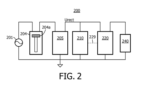
[0025] FIG. 2 is a block diagram showing a dimmable lighting system, according
to a
representative embodiment.
[0026] FIGs. 3A and 3B show sample waveforms and corresponding digital pulses
from
asymmetric half cycles of a dimmer, according to a representative embodiment.
[0027] FIG. 4 is a flow diagram showing a process of detecting and correcting
improper
operation of a dimmable lighting system, according to a representative
embodiment.
[0028] FIG. 5 is a flow diagram showing a process of identifying and
implementing
corrective actions, according to a representative embodiment.
[0029] FIG. 6 is a circuit diagram showing a control circuit for a lighting
system,
according to a representative embodiment.
[0030] FIGs. 7A-7C show sample waveforms and corresponding digital pulses of a
dimmer, according to a representative embodiment.
[0031] FIG. 8 is a flow diagram showing a process of detecting phase angles,
according
to a representative embodiment.
CA 02799631 2012-11-15
WO 2011/145009 PCT/IB2011/051806
-9-
Detailed Description
[0032] In the following detailed description, for purposes of explanation and
not
limitation, representative embodiments disclosing specific details are set
forth in order to
provide a thorough understanding of the present teachings. However, it will be
apparent to
one having ordinary skill in the art having had the benefit of the present
disclosure that other
embodiments according to the present teachings that depart from the specific
details
disclosed herein remain within the scope of the appended claims. Moreover,
descriptions of
well-known apparatuses and methods may be omitted so as to not obscure the
description of
the representative embodiments. Such methods and apparatuses are clearly
within the scope
of the present teachings.
[0033] Generally, it is desirable to have steady light output from a solid
state lighting
load, such as an LED light source, e.g., without flicker or uncontrolled
fluctuation in output
light levels, regardless of dimmer settings. Applicant has recognized and
appreciated that it
would be beneficial to provide a circuit capable of detecting and correcting
various problems
caused by a dimmer and a solid state lighting load and corresponding power
converter driving
the solid state lighting load. In various embodiments, the problems may be
detected by
identifying asymmetries in positive and negative mains half cycles, e.g., due
to an interaction
between an electronic transformer or power converter and a phase chopping
dimmer.
[0034] In view of the foregoing, various embodiments and implementations of
the
present invention are directed to a circuit and method for detecting and
correcting improper
operation of solid state lighting fixtures caused by asymmetries in positive
and negative mains
half cycles, by digitally detecting and measuring the phase angle of the
dimmer, and
implementing corrective action when a difference between consecutive
measurements (e.g.,
respectively corresponding to positive and negative half-cycles) exceeds a
predetermined
threshold, indicating asymmetrical phase chopping.
[0035] FIG. 2 is a block diagram showing a dimmable lighting system, according
to a
representative embodiment. Referring to FIG. 2, lighting system 200 includes
dimmer 204 and
rectification circuit 205, which provide a (dimmed) rectified voltage Urect
from voltage mains
201. The voltage mains 201 may provide different unrectified input mains
voltages, such as
CA 02799631 2012-11-15
WO 2011/145009 PCT/IB2011/051806
-10-
100VAC, 120VAC, 230VAC and 277VAC, according to various implementations. The
dimmer
204 is a phase chopping dimmer, for example, which provides dimming capability
by chopping
trailing edges (trailing edge dimmer) or leading edges (leading edge dimmer)
of voltage signal
waveforms from the voltage mains 201 in response to vertical operation of its
slider 204a. For
purposes of discussion, it is assumed that the dimmer 204 is a trailing edge
dimmer.
[0036] Generally, the magnitude of the rectified voltage Urect is proportional
to a
phase angle or level of dimming set by the dimmer 204, such that a phase angle
corresponding
to a lower dimmer setting results in a lower rectified voltage Urect and vice
versa. In the
depicted example, it may be assumed that the slider 204a is moved downward to
lower the
phase angle, reducing the amount of light output by solid state lighting load
240, and is moved
upward to increase the phase angle, increasing the amount of light output by
the solid state
lighting load 240. Therefore, the least dimming occurs when the slider 204a is
at the top
position (as depicted in FIG. 2), and the most dimming occurs when the slider
204a is at its
bottom position.
[0037] The lighting system 200 further includes dimmer phase angle detection
circuit
210 and power converter 220. The phase angle detection circuit 210 includes a
microcontroller or other controller, discussed below, and is configured to
determine or
measure values of the phase angle (dimming level) of the representative dimmer
204 based on
the rectified voltage Urect. The phase angle detection circuit 210 also
compares detected
phase angle values corresponding to positive and negative half cycles of the
rectified voltage
Urect, and implements corrective action if the comparison of the positive and
negative half
cycles indicates that the lighting system 200 is operating improperly. For
example, the
detected phase angle may be used as an input to a software algorithm to
determine whether
the chopped waveforms of the rectified voltage Urect are being chopped
symmetrically (e.g.,
as shown in FIG. 1B) or asymmetrically (as shown in FIG. 1C). Stated
differently, it is
determined whether the chopped waveforms are symmetric or asymmetric.
Asymmetrical
chopping is indicative of a problem with the dimmer-driver system, e.g.,
including the dimmer
204 and the power converter 220. In various embodiments, the phase angle
detection circuit
210 may be further configured to adjust dynamically an operating point of the
power
CA 02799631 2012-11-15
WO 2011/145009 PCT/IB2011/051806
-11-
converter 220 during normal operations based, in part, on the detected phase
angles, using a
power control signal via control line 229.
[0038] Generally, asymmetries in the chopped waveforms can be detected by
detecting large differences in lengths of phase angle detection pulses,
generated by the phase
angle detection circuit 210, from positive half cycles to negative half
cycles. For example, FIGs.
3A and 3B show chopped waveforms from the dimmer 204 and the rectification
circuit 205
corresponding to positive and negative half cycles of the rectified voltage
Urect, and
associated digital pulses generated by the phase angle detection circuit 210,
according to a
representative embodiment. As shown in FIG. 3B, the length of the second
digital pulse 332b
is significantly smaller than the length of the first digital pulse 331b,
indicating that the
negative half cycle waveform 332a is more heavily chopped than the immediately
preceding
positive half cycle waveform 331a, as shown in FIG. 3A.
[0039] Typically, when a user manually operates the dimmer 204 by adjusting
the
slider 204a, the result has a very slow and gradual effect on the differences
between positive
and negative half cycles. Therefore, a more drastic change from one cycle to
another cycle, as
shown for example in FIGs. 3A and 3B, is distinguishable as improper
operation. In an
embodiment, a difference threshold may be established, e.g., based on
empirical
measurements, which indicates the upper limit of tolerable differences between
positive and
negative half cycles. For example, the difference threshold may be the point
at which flicker
begins to occur based on the asymmetrical waveforms. As discussed below with
respect to
FIG. 4, the phase angle detection circuit 210 (e.g., using the microcontroller
or other
controller) may compare differences between the digital pulses of positive and
negative half
cycles with the difference threshold, and identify occurrences of improper
operation when the
differences exceed the difference threshold.
[0040] Because an asymmetrical waveform is a symptom of multiple potential
problems, all of which result in the undesirable flicker in the light output
from the solid state
lighting load 240, different corrective actions or methods can be attempted
under control of
the phase angle detection circuit 210 to correct the problem. For example, the
phase angle
detection circuit 210 may switch in a resistive bleeder circuit (not shown in
FIG. 2), in parallel
CA 02799631 2012-11-15
WO 2011/145009 PCT/IB2011/051806
-12-
with the solid state lighting load 240, to draw extra current along with the
solid state lighting
load 240, thus increasing the load to a sufficient minimum for operation of
the dimmer 204. If
this action does not correct the flicker or the underlying issue, other
corrective actions may be
attempted. The corrective actions may be attempted in a predetermined order of
priority,
e.g., from most likely to least likely to be successful, until one of the
corrective actions works.
However, if no corrective actions work, the phase angle detection circuit 210
may simply shut
down the power converter 220 using a power control signal sent via control
line 229, since no
light may be more desirable than flickering light. For example, the phase
angle detection
circuit 210 may control the power converter 220 to deliver no current to the
solid state lighting
load 240, or may cause the power converter 220 to shut off.
[0041] The power converter 220 receives the rectified voltage Urect from the
rectification circuit 205 and the power control signal via the control line
229, and outputs a
corresponding DC voltage for powering the solid state lighting load 240.
Generally, the power
converter 220 converts between the rectified voltage Urect and the DC voltage
based on at
least the magnitude of the rectified voltage Urect and the value of the power
control signal
received from the phase angle detection circuit 210. DC voltage output by the
power
converter 220 thus reflects the rectified voltage Urect and the dimmer phase
angle applied by
the dimmer 204. In various embodiments, the power converter 220 operates in an
open loop
or feed-forward fashion, as described in U.S. Patent No. 7,256,554 to Lys, for
example, which is
hereby incorporated by reference.
[0042] In various embodiments, the power control signal may be a pulse width
modulation (PWM) signal, for example, which alternates between high and low
levels in
accordance with a selected duty cycle. For example, the power control signal
may have a high
duty cycle (e.g., 100 percent) corresponding to a maximum on-time (high phase
angle) of the
dimmer 204, and a low duty cycle (e.g., 0 percent) corresponding to a minimum
on-time (low
phase angle) of the dimmer 204. When the dimmer 204 is set in between maximum
and
minimum phase angles, the phase angle detection circuit 210 determines a duty
cycle of the
power control signal that specifically corresponds to the detected phase
angle.
CA 02799631 2012-11-15
WO 2011/145009 PCT/IB2011/051806
-13-
[0043] FIG. 4 is a flow diagram showing a process of detecting improper
operation of a
dimmable lighting system, according to a representative embodiment. The
process may be
implemented, for example, by firmware and/or software executed by phase angle
detection
circuit 210 shown in FIG. 2 (or by microcontroller 615 of FIG. 6, discussed
below).
[0044] It may be assumed for purposes of explanation that FIG. 4 begins at
block S410
when the lighting system 200 is powered on. In block S410, there is a delay
while the rectified
input mains voltage Urect reaches steady state. After the delay, an initial
value of the phase
angle is determined and saved as the Previous Half Cycle Level in block S420.
For example, the
initial value of the phase angle may be determined by simply detecting the
phase angle,
according to the process discussed below with reference to block S430.
Alternatively, the
initial value of the phase angle may be determined according to other
processes or may be
retrieved from memory storing a previously determined phase angle, e.g., from
prior
operation of the lighting system 200, without departing from the scope of the
present
teachings.
[0045] In the process indicated by block S430, the phase angle detection
circuit 210
detects the phase angle, in order to determine or measure another value of the
phase angle.
In various embodiments, the phase angle is detected by obtaining a digital
pulse
corresponding to each chopped waveform of the rectified input mains voltage
Urect, according
to the algorithm discussed below with reference to FIGs. 6-8, for example.
Therefore, a digital
pulse is generated for each positive half cycle and negative half cycle, as
shown in FIGs. 3A and
3B. Of course, the value of the phase angle may be determined according to
other processes,
without departing from the scope of the present teachings.
[0046] The detected phase angle is saved as the Current Half Cycle Level in
block S440.
The Previous Half Cycle Level and the Current Half Cycle Level may be stored
in memory. For
example, the memory may be an external memory or a memory internal to the
phase angle
detection circuit 210 and/or a microcontroller or other controller included in
the phase angle
detection circuit 210, as discussed below with reference to FIG. 6. In various
embodiments,
values of the Previous Half Cycle Level and the Current Half Cycle Level may
be used to
populate tables or may be saved in a relational database for comparison,
although other
CA 02799631 2012-11-15
WO 2011/145009 PCT/IB2011/051806
-14-
means of storing the Previous Half Cycle Level and the Current Half Cycle
Level may be
incorporated without departing from the scope of the present teachings. Also,
in various
embodiments, the value of the phase angle detected in block S430 may be used
by the phase
angle detection circuit 210 to generate a power control signal, which is
provided to the power
controller 220 to set an operating point of the power controller 220, enabling
further control
over the light output by the solid state lighting load 240 based on various
other control
criteria.
[0047] The difference ADim between the Current Half Cycle Level and the
Previous Half
Cycle Level is determined in block S450, for example, by subtracting the
Current Half Cycle
Level from the Previous Half Cycle Level, or vice versa. The difference ADim
is then compared
to a predetermined difference threshold AThreshold in block S460 to determine
whether the
waveforms are asymmetric, e.g., indicating incompatibility between or improper
operation of
the dimmer 204 and/or the power converter 220. When the difference ADim is
greater than
the threshold AThreshold (block S460: Yes), indicating asymmetric waveforms, a
process
indicated by block S480 is performed in order to identify and implement an
appropriate
corrective action to address the problem causing the asymmetrical waveforms.
This process is
described in detail with reference to FIG. 5, below. When the difference ADim
is not greater
than the threshold AThreshold (block S460: No), indicating substantially
symmetric waveforms,
the Current Half Cycle Level is simply saved as the Previous Half Cycle Level
in block S470. The
process then returns to block S430 to determine again the phase angle, and the
process
indicated by blocks S440-S480 is repeated.
[0048] FIG. 5 is a flow diagram showing a process of identifying and
implementing
corrective actions in response to the detection of asynchronous waveforms,
according to a
representative embodiment. The process may be implemented, for example, by
firmware
and/or software executed by phase angle detection circuit 210 shown in FIG. 2
(or by
microcontroller 615 of FIG. 6 or other controller, discussed below).
[0049] In various embodiments, one or more corrective actions are available
for
implementation, as needed. The corrective actions may be ranked in order from
highest to
lowest priority, where the highest priority corrective action is the
corrective action previously
CA 02799631 2012-11-15
WO 2011/145009 PCT/IB2011/051806
-15-
determined to be the most likely to address successfully the asymmetrical
waveforms. The
ranking, along with corresponding steps to be executed for implementation of
each of the
corrective actions, may be stored in memory. For example, the memory may be an
external
memory or a memory internal to the phase angle detection circuit 210 and/or a
microcontroller or other controller included in the phase angle detection
circuit 210, as
discussed below with reference to FIG. 6. The highest priority corrective
action may include
switching in a resistive bleeder circuit in parallel with the solid state
lighting load 240, for
example, to increase the load of the dimmer 204 to a sufficient minimum load.
The resistive
bleeder circuit may include a resistance connected in series with a switch
(e.g., a transistor),
for example, to selectively draw additional current. One or more additional
corrective actions,
the implementation of which would be apparent to one of ordinary skill in the
art, may be
prioritized below the resistive bleeder circuit corrective action. In
addition, one or more
variations of the same corrective action may be prioritized. For example,
implementation of
the resistive bleeder circuit may be repeated using incrementally increasing
resistance values,
until an appropriate value is found.
[0050] Referring to FIG. 5, it is determined in block S481 whether a
corrective action is
already actively in place. When there is no corrective action in place (block
S481: No), the
highest priority corrective action is implemented in block S482, and the
process returns to
block S470 of FIG. 4, where the Current Half Cycle Level is saved as the
Previous Half Cycle
Level. The process then returns to block S430 to determine again the phase
angle as the
Current Half Cycle Level, the subsequent comparison of which to the Previous
Half Cycle Level
in blocks S450 and S460 indicates whether the corrective action implemented in
block S482 is
successful. As a practical matter, one or more half cycles may be evaluated
after
implementing a corrective action in order to allow the corrective action to
take effect before
making a determination as to the success of that action.
[0051] Referring again to FIG. 5, when it is determined that there is already
a
corrective action in place (block S481: Yes), it is then determined whether
there are any
remaining corrective actions that may be attempted in block S483. When there
is at least one
remaining corrective action (block S483: Yes), the next highest priority
corrective action is
CA 02799631 2012-11-15
WO 2011/145009 PCT/IB2011/051806
-16-
implemented in block S485, and the process returns to block S470 of FIG. 4, as
discussed
above.
[0052] When there are not more corrective actions (block S483: No), the power
converter 220 is shut down in block S486, in order to eliminate the flickering
light output from
the solid state lighting load 240 or other adverse affect of the improper
operation. The
process then returns to block S470 of FIG. 4, where the monitoring process may
be repeated,
even though the power converter 220 is shut down. Although not shown in FIGs.
4 and 5, in
various embodiments, the power converter 220 may be turned on again if
subsequent
comparisons between the Current and Previous Half Cycle Levels indicate that
the difference
ADim drops below the threshold AThreshold, which may occur in response to
further
adjustments to the dimming level, e.g., through manipulation of the slider
204a.
[0053] In various embodiments, each time the lighting system 200 is powered
on, the
power converter 220 is on and no corrective actions are in place. In other
words, any
corrective action that may have been activated in a previous operation of the
lighting system
200 is discontinued when the lighting system 200 is powered off. Likewise, any
determination
that the flicker could not be corrected using the available corrective
actions, resulting in the
power converter 220 being shut down, is not carried forward to subsequent
operations of the
lighting system 200. Of course, in alternative embodiments, corrective actions
and/or
determinations to shut down the power converter 220 may be carried forward or
otherwise
considered with respect to subsequent operations, without departing from the
scope of the
present teachings. For example, if a particular corrective action is found to
adequately address
the flickering of light output by the solid state lighting load 240, the
priority ranking of the
available corrective actions may be reordered so that the successful
corrective action has the
highest priority.
[0054] Further, FIG. 4 depicts an embodiment in which the process takes place
continuously throughout operation of the lighting system 200. However, in
alternative
embodiments, the process of FIG. 4 may occur only during an initial start-up
period, during
which the difference ADim between the Current Half Cycle Level and the
Previous Half Cycle
Level is determined and compared with the difference threshold AThreshold,
based on
CA 02799631 2012-11-15
WO 2011/145009 PCT/IB2011/051806
-17-
detected values of the phase angle. If no corrective actions are identified
and implemented in
response to the comparison (i.e., the waveforms of the input mains voltage
signal are
symmetrical), the process ends and the lighting system 200 operates in
response to the
dimmer 204 without further analysis of the difference ADim between the Current
and Previous
Half Cycle Levels. Likewise, if a corrective action is identified and
successfully implemented
(i.e., in response to the waveforms of the input mains voltage signal being
asymmetrical), the
process ends and the lighting system 200 operates in response to the dimmer
204 using the
corrective action without further analysis of the difference ADim between the
Current and
Previous Half Cycle Levels. In this manner, a corrective action, such as
switching in a resistive
bleeder circuit, is implemented to correct the problem for the remainder of
the operation
without expending the additional processing power to conduct further checks.
[0055] FIG. 6 is a circuit diagram showing a control circuit for a dimmable
lighting
system, including a phase angle detection circuit, a power converter and a
solid state lighting
fixture, according to a representative embodiment. The general components of
FIG. 6 are
similar to those of FIG. 2, although more detail is provided with respect to
various
representative components, in accordance with an illustrative configuration.
Of course, other
configurations may be implemented without departing from the scope of the
present
teachings.
[0056] Referring to FIG. 6, control circuit 600 includes rectification circuit
605 and
phase angle detection circuit 610 (dashed box). As discussed above with
respect to the
rectification circuit 205, the rectification circuit 605 is connected to a
dimmer connected
between the rectification circuit 605 and the voltage mains to receive
(dimmed) unrectified
voltage, indicated by the dimmed hot and neutral inputs. In the depicted
configuration, the
rectification circuit 605 includes four diodes D601-D604 connected between
rectified voltage
node N2 and ground. The rectified voltage node N2 receives the rectified
voltage Urect, and is
connected to ground through input filtering capacitor C615 connected in
parallel with the
rectification circuit 605.
[0057] The phase angle detection circuit 610 performs a phase angle detection
process
based on the rectified voltage Urect. The phase angle corresponding to the
level of dimming
CA 02799631 2012-11-15
WO 2011/145009 PCT/IB2011/051806
-18-
set by the dimmer is detected based on the extent of phase chopping present in
a signal
waveform of the rectified voltage Urect. The power converter 620 controls
operation of the
LED load 640, which includes representative LEDs 641 and 642 connected in
series, based on
the rectified voltage Urect (RMS input voltage) and, in various embodiments, a
power control
signal provided by the phase angle detection circuit 610 via control line 629.
This allows the
phase angle detection circuit 610 to adjust the power delivered from the power
converter 620
to the LED load 640. The power control signal may be a PWM signal or other
digital signal, for
example. In various embodiments, the power converter 620 operates in an open
loop or feed-
forward fashion, as described in U.S. Patent No. 7,256,554 to Lys, for
example, which is hereby
incorporated by reference.
[0058] In the depicted representative embodiment, the phase angle detection
circuit
610 includes microcontroller 615, which uses signal waveforms of the rectified
voltage Urect
to determine the phase angle. The microcontroller 615 includes digital input
618 connected
between a first diode D611 and a second diode D612. The first diode D611 has
an anode
connected to the digital input 618 and a cathode connected to voltage source
Vcc, and the
second diode D612 has an anode connected to ground and a cathode connected to
the digital
input 618. The microcontroller 615 also includes the digital output 619.
[0059] In various embodiments, the microcontroller 615 may be a PIC12F683,
available
from Microchip Technology, Inc., and the power converter 620 may be an L6562,
available
from ST Microelectronics, for example, although other types of
microcontrollers, power
converters, or other processors and/or controllers may be included without
departing from
the scope of the present teachings. For example, the functionality of the
microcontroller 615
may be implemented by one or more processors and/or controllers, connected to
receive
digital input between first and second diodes D611 and D612 as discussed
above, and which
may be programmed using software or firmware (e.g., stored in a memory) to
perform the
various functions described herein, or may be implemented as a combination of
dedicated
hardware to perform some functions and a processor (e.g., one or more
programmed
microprocessors and associated circuitry) to perform other functions. Examples
of controller
CA 02799631 2012-11-15
WO 2011/145009 PCT/IB2011/051806
-19-
components that may be employed in various embodiments include, but are not
limited to,
conventional microprocessors, microcontrollers, ASICs and FPGAs, as discussed
above.
[0060] The phase angle detection circuit 610 further includes various passive
electronic
components, such as first and second capacitors C613 and C614, and a
resistance indicated by
representative first and second resistors R611 and R612. The first capacitor
C613 is connected
between the digital input 618 of the microcontroller 615 and a detection node
N1. The second
capacitor C614 is connected between the detection node N1 and ground. The
first and second
resistors R611 and R612 are connected in series between the rectified voltage
node N2 and
the detection node N1. In the depicted embodiment, the first capacitor C613
may have a
value of about 560pF and the second capacitor C614 may have a value of about
10pF, for
example. Also, the first resistor R611 may have a value of about 1 megohm and
the second
resistor R612 may have a value of about 1 megohm, for example. However, the
respective
values of the first and second capacitors C613 and C614, and the first and
second resistors
R611 and R612 may vary to provide unique benefits for any particular situation
or to meet
application specific design requirements of various implementations, as would
be apparent to
one of ordinary skill in the art.
[0061] The rectified voltage Urect is AC coupled to the digital input 618 of
the
microcontroller 615. The first resistor R611 and the second resistor R612
limit the current into
the digital input 618. When a signal waveform of the rectified voltage Urect
goes high, the
first capacitor C613 is charged on the rising edge through the first and
second resistors R611
and R612. The first diode D611 clamps the digital input 618 one diode drop
above the voltage
source Vcc, for example, while the first capacitor C613 is charged. The first
capacitor C613
remains charged as long as the signal waveform is not zero. On the falling
edge of the signal
waveform of the rectified voltage Urect, the first capacitor C613 discharges
through the
second capacitor C614, and the digital input 618 is clamped to one diode drop
below ground
by the second diode D612. When a trailing edge dimmer is used, the falling
edge of the signal
waveform corresponds to the beginning of the chopped portion of the waveform.
The first
capacitor C613 remains discharged as long as the signal waveform is zero.
Accordingly, the
CA 02799631 2012-11-15
WO 2011/145009 PCT/IB2011/051806
-20-
resulting logic level digital pulse at the digital input 618 closely follows
the movement of the
chopped rectified voltage Urect, examples of which are shown in FIGs. 7A-7C.
[0062] More particularly, FIGs. 7A-7C show sample waveforms and corresponding
digital pulses at the digital input 618, according to representative
embodiments. The top
waveforms in each figure depict the chopped rectified voltage Urect, where the
amount of
chopping reflects the level of dimming. For example, the waveforms may depict
a portion of a
full 170V (or 340V for E.U.) peak, rectified sine wave that appears at the
output of the dimmer.
The bottom square waveforms depict the corresponding digital pulses seen at
the digital input
618 of the microcontroller 615. Notably, the length of each digital pulse
corresponds to a
chopped waveform, and thus is equal to the dimmer on-time (e.g., the amount of
time the
dimmer's internal switch is "on"). By receiving the digital pulses via the
digital input 618, the
microcontroller 615 is able to determine the level to which the dimmer has
been set.
[0063] FIG. 7A shows sample waveforms of rectified voltage Urect and
corresponding
digital pulses when the dimmer is at about its maximum setting, indicated by
the top position
of the dimmer slider shown next to the waveforms. FIG. 7B shows sample
waveforms of
rectified voltage Urect and corresponding digital pulses when the dimmer is at
a medium
setting, indicated by the middle position of the dimmer slider shown next to
the waveforms.
FIG. 7C shows sample waveforms of rectified voltage Urect and corresponding
digital pulses
when the dimmer is at about its minimum setting, indicated by the bottom
position of the
dimmer slider shown next to the waveforms.
[0064] FIG. 8 is a flow diagram showing a process of detecting the phase angle
of a
dimmer, according to a representative embodiment. The process may be
implemented by
firmware and/or software executed by the microcontroller 615 shown in FIG. 6,
or more
generally by a processor or controller, e.g., the phase angle detection
circuit 210 shown in FIG.
2, for example.
[0065] In block S821 of FIG. 8, a rising edge of a digital pulse of an input
signal (e.g.,
indicated by rising edges of the bottom waveforms in FIGs. 7A-7C) is detected,
for example, by
initial charging of the first capacitor C613. Sampling at the digital input
618 of the
CA 02799631 2012-11-15
WO 2011/145009 PCT/IB2011/051806
-21-
microcontroller 615, for example, begins in block S822. In the depicted
embodiment, the
signal is sampled digitally for a predetermined time equal to just under a
mains half cycle.
Each time the signal is sampled, it is determined in block S823 whether the
sample has a high
level (e.g., digital "1") or a low level (e.g., digital "0"). In the depicted
embodiment, a
comparison is made in block S823 to determine whether the sample is digital
"1." When the
sample is digital "1" (block S823: Yes), a counter is incremented in block
S824, and when the
sample is not digital "1" (block S823: No), a small delay is inserted in block
S825. The delay is
inserted so that the number of clock cycles (e.g., of the microcontroller 615)
is equal
regardless of whether the sample is determined to be digital "1" or digital
"0."
[0066] In block S826, it is determined whether the entire mains half cycle has
been
sampled. When the mains half cycle is not complete (block S826: No), the
process returns to
block S822 to again sample the signal at the digital input 618. When the mains
half cycle is
complete (block S826: Yes), the sampling stops and the counter value
accumulated in block
S824 is identified as the current value of the phase angle in block S827, and
the counter is
reset to zero. The counter value may be stored in a memory, examples of which
are discussed
above. The microcontroller 615 may then wait for the next rising edge to begin
sampling
again. For example, it may be assumed that the microcontroller 615 takes 255
samples during
a mains half cycle. When the dimmer phase angle is set by the slider at the
top of its range
(e.g., as shown in FIG. 7A), the counter will increment to about 255 in block
S824 of FIG. 8.
When the dimmer phase angle is set by the slider at the bottom of its range
(e.g., as shown in
FIG. 7C), the counter will increment to only about 10 or 20 in block S824.
When the dimmer
phase angle is set somewhere in the middle of its range (e.g., as shown in
FIG. 7B), the counter
will increment to about 128 in block S824. The value of the counter thus gives
the
microcontroller 615 an accurate indication of the level to which the dimmer
has been set or
the phase angle of the dimmer. In various embodiments, the value of the phase
angle may be
calculated, e.g., by the microcontroller 615, using a predetermined function
of the counter
value, where the function may vary in order to provide unique benefits for any
particular
situation or to meet application specific design requirements of various
implementations, as
would be apparent to one of ordinary skill in the art.
CA 02799631 2012-11-15
WO 2011/145009 PCT/IB2011/051806
-22-
[0067] Referring again to FIG. 6, the microcontroller 615 may also be
configured to
detect improper operation of the dimmer (not shown) and/or the power converter
620,
causing the LED load 640 to output flickering light, and to identify and
implement corrective
action, as discussed above with reference to FIGs. 4 and 5. In the depicted
example, the
control circuit 600 includes representative resistive bleeder circuit 650,
which is assumed to be
the highest priority corrective action for purposes of explanation. The
resistive bleeder circuit
650 includes resistor 652 connected in series with a switch, depicted as
transistor 651. The
transistor 651 is shown as a field effect transistor (FET), for example, such
as a metal-oxide-
semiconductor field-effect transistor (MOSFET) or gallium arsenide field-
effect transistor (GaAs
FET), although other types of FETs and/or other types of transistors within
the purview of one
of ordinary skill in the art may be incorporated, without departing from the
scope of the
present teachings.
[0068] A gate of the transistor 651 is connected to the microcontroller 615
via control
line 659. Thus, the microcontroller 615 is selectively able to turn on the
transistor 651 in order
to switch in the resistive bleeder circuit 650 (e.g., in accordance with block
S482 of FIG. 5) and
to turn off the transistor 651 to switch out the resistive bleeder circuit
650, for example, to
implement the next highest priority corrective action (e.g., in accordance
with block S485 of
FIG. 5). When the transistor 651 is turned on, the resistance of the resistor
R652 is connected
in parallel with the LED load 640 to draw additional current and to increase
the load of the
dimmer. Also, as discussed above, when the corrective action(s), including
implementation of
the resistive bleeder circuit 650, are not successful, the microcontroller 615
may be configured
to shut down the power converter 620, for example, via control line 629. In
addition, the
microcontroller 615 may be configured to execute one or more additional
control algorithms
to adjust dynamically an operating point of the power converter 620 based, at
least in part, on
the detected phase angles, using a power control signal via the control line
629.
[0069] Generally, it is contemplated to ensure that flickering does not occur
in the light
output by a solid state lighting fixture due to incompatibility between the
drivers (e.g., power
converters) and phase chopping dimmers. According to various embodiments, a
process
detects improper operation, attempts to correct it, and shuts off the light
output by the solid
CA 02799631 2012-11-15
WO 2011/145009 PCT/IB2011/051806
-23-
state lighting fixture (e.g., by shutting down the power converter) if the
improper operation is
not resolved by the attempted corrections. Accordingly, flicker can be
eliminated, and the
power converter is able to work with various different dimmers without being
limited by
potential incompatibility.
[0070] In various embodiments, the functionality of the phase angle detection
circuit
210 and/or the microcontroller 615, for example, may be implemented by one or
more
processing circuits, constructed of any combination of hardware, firmware or
software
architectures, and may include its own memory (e.g., nonvolatile memory) for
storing
executable software/firmware executable code that allows it to perform the
various functions.
For example, the functionality may be implemented using ASICs, FPGAs, and the
like.
[0071] Detecting and correcting improper dimmer operation, e.g., indicated by
asymmetrical positive and negative half cycles of input mains voltage signals,
can be used with
any dimmable power converter with a solid state lighting (e.g., LED) load
where it is desired to
eliminate light flicker, or otherwise to increase compatibility with a variety
of phase chopping
dimmers. The phase angle detection circuit, according to various embodiments,
may be
implemented in various LED-based light sources. Further, it may be used as a
building block of
"smart" improvements to various products to make them more dimmer-friendly.
[0072] While multiple inventive embodiments have been described and
illustrated
herein, those of ordinary skill in the art will readily envision a variety of
other means and/or
structures for performing the function and/or obtaining the results and/or one
or more of the
advantages described herein, and each of such variations and/or modifications
is deemed to
be within the scope of the inventive embodiments described herein. More
generally, those
skilled in the art will readily appreciate that all parameters, dimensions,
materials, and
configurations described herein are meant to be exemplary and that the actual
parameters,
dimensions, materials, and/or configurations will depend upon the specific
application or
applications for which the inventive teachings is/are used.
[0073] Those skilled in the art will recognize, or be able to ascertain using
no more
than routine experimentation, many equivalents to the specific inventive
embodiments
CA 02799631 2012-11-15
WO 2011/145009 PCT/IB2011/051806
-24-
described herein. It is, therefore, to be understood that the foregoing
embodiments are
presented by way of example only and that, within the scope of the appended
claims and
equivalents thereto, inventive embodiments may be practiced otherwise than as
specifically
described and claimed. Inventive embodiments of the present disclosure are
directed to each
individual feature, system, article, material, kit, and/or method described
herein. In addition,
any combination of two or more such features, systems, articles, materials,
kits, and/or
methods, if such features, systems, articles, materials, kits, and/or methods
are not mutually
inconsistent, is included within the inventive scope of the present
disclosure.
[0074] All definitions, as defined and used herein, should be understood to
control
over dictionary definitions, definitions in documents incorporated by
reference, and/or
ordinary meanings of the defined terms.
[0075] The indefinite articles "a" and "an," as used herein in the
specification and in
the claims, unless clearly indicated to the contrary, should be understood to
mean "at least
one." As used herein in the specification and in the claims, the phrase "at
least one," in
reference to a list of one or more elements, should be understood to mean at
least one
element selected from any one or more of the elements in the list of elements,
but not
necessarily including at least one of each and every element specifically
listed within the list of
elements and not excluding any combinations of elements in the list of
elements. This
definition also allows that elements may optionally be present other than the
elements
specifically identified within the list of elements to which the phrase "at
least one" refers,
whether related or unrelated to those elements specifically identified. Thus,
as a non-limiting
example, "at least one of A and B" (or, equivalently, "at least one of A or
B," or, equivalently
"at least one of A and/or B") can refer, in one embodiment, to at least one,
optionally
including more than one, A, with no B present (and optionally including
elements other than
B); in another embodiment, to at least one, optionally including more than
one, B, with no A
present (and optionally including elements other than A); in yet another
embodiment, to at
least one, optionally including more than one, A, and at least one, optionally
including more
than one, B (and optionally including other elements); etc.
CA 02799631 2012-11-15
WO 2011/145009 PCT/IB2011/051806
-25-
[0076] It should also be understood that, unless clearly indicated to the
contrary, in
any methods claimed herein that include more than one step or act, the order
of the steps or
acts of the method is not necessarily limited to the order in which the steps
or acts of the
method are recited. Also, any reference numerals or other characters,
appearing between
parentheses in the claims, are provided merely for convenience and are not
intended to limit
the claims in any way,
[0077] In the claims, as well as in the specification above, all transitional
phrases such
as "comprising," "including," "carrying," "having," "containing," "involving,"
"holding,"
"composed of," and the like are to be understood to be open-ended, i.e., to
mean including
but not limited to. Only the transitional phrases "consisting of" and
"consisting essentially of"
shall be closed or semi-closed transitional phrases, respectively.