Note: Descriptions are shown in the official language in which they were submitted.
CA 02799658 2014-12-05
1000-029
CONTROL APPARATUS AND LIGHTING APPARATUS
INCORPORATING CONTROL APPARATUS
CROSS-REFERENCE TO RELATED APPLICATION
The present application is a Canadian national entty of PCT Patent Application
No.
PCT/CA2011/000524 filed on May 11, 2011.
FIELD OF THE INVENTION
The invention relates generally to control systems and, more particularly, to
control
apparatus, lighting control apparatus and lighting apparatus incorporating
control
apparatus.
BACKGROUND
Light Emitting Diodes (LEDs) are increasingly being adopted as general
illumination
lighting sources due to their high energy efficiency and long service life
relative to
traditional sources of light such as incandescent, fluorescent and halogen.
Each
generation of LEDs are providing improvenients in energy efficiency and cost
per
lumen, thus allowing for lighting manufacturers to produce LED light fixtures
at
increasingly cost competitive prices. These reduced costs are expanding the
applications of LED lighting from niche markets, such as outdoor street
lighting,
Christmas lights and flashlights, to general illumination within offices,
retail,
industrial, and residential environments. Within these environments, users
typically
want an LED light fixture to operate in substantially the same manner as their
current
lighting solution with at least a similar set of functionality.
Within many applications for lighting, users desire the ability to adjust the
intensity of
a light fixture. Changes in intensity may be desired for a large number of
reasons
including to create a particular mood, to reduce energy, to adjust for other
sources of
light (ex. ambient sunlight), to reduce glare on objects (ex. televisions) or
for another
lighting effect. For incandescent lighting solutions, the most common control
device
for controlling the intensity of a light fixture is a dimmer that contains
electrical
circuits including a TRIAC and/or DIAC, the dimmer typically being called a
TRIAC
dirruner. One skilled in the art would understand that a TRIAC dimmer is
typically
CA 02799658 2012-11-13
WO 2011/140631
PCT/CA2011/000524
implemented in series within the AC power line and cuts off portions of the AC
power sine wave based on the setting of a potentiometer. The modified AC
signal
powers the incandescent light fixture at a lower power level than a full AC
signal
would have otherwise, thus lower lumens are projected from the light fixture.
LED light fixtures that initially were on the market could not operate with
traditional
TRIAC dimmers. Instead, custom dimming controllers were developed to
interoperate with LED light fixtures to control a pulse width modulated (PWM)
signal
that could be used to adjust the intensity of the LEDs. A key problem is these
custom
dimmers can be considerably more expensive than standard TRIAC dimmers. This
increase in cost is due to the incredible economies of scale that currently
benefit
TRIAC dimmers.
To overcome this cost dilemma and to reuse the TRIAC dimmer products and form
factors that are currently on the market, a number of solutions have been
developed to
use standard TRIAC dimmers with LED lighting fixtures. For example, National
Semiconductor of Santa Clara, CA, U.S.A. has developed a TRIAC dimmable
offline
LED driver LM3445 which can be implemented within a constant current
architecture
to illuminate high power LEDs. This component includes a TRIAC dim decoder
which can interpret the setting on the TRIAC dimmer and enable it to control
the
output current to the LEDs.
One problem with these solutions is related to the fundamental operation of
the
standard TRIAC dimmers. A TRIAC dimmer in operation generates a modified
sinusoid in which portions of the waveform have been cut-off (or zeroed). When
rectified within an AC/DC converter, the resulting DC power level requires
additional
components to ensure a constant voltage level is applied to the resulting
LEDs. These
additional components add inefficiencies to the system. Further, the TRIAC
within
the dimmer requires a holding current throughout the AC line cycle in order to
operate
properly. To maintain this holding current, additional resistors are required
to create a
load for the TRIAC. This load wastes power and reduces the efficiency of the
overall
light fixture.
2
CA 02799658 2012-11-13
WO 2011/140631
PCT/CA2011/000524
Another problem with the current implementations of TRIAC dimmers as they
relate
to control of LED light fixtures is that these architectures are limited to
controlling the
intensity of the light fixture. Since the use of the TRIAC dimmer, as
currently
developed, reduces the power applied to the light fixture, the current TRIAC
dimmer
solutions do not operate well when the information being conveyed with the
TRIAC
dimmer is not intensity information but information related to another aspect
of the
light fixture, such as color or color temperature.
Additionally, certain lighting systems, including lighting systems employing
LEDs,
that are currently available have control systems that are designed to work
with a 0-
10V dimmer. It would be desirable to provide a control apparatus that may be
used
with a TRIAC dimmer to provide a variable voltage control signal so that
control
systems of this nature may be readily adapted for use with TRIAC dimmers.
Against this background, there is a need for solutions that will better
control LEDs
within a lighting apparatus in order to adjust aspects, such as intensity,
color and/or
color temperature, of the light output. Further, solutions that re-use
existing lighting
control interfaces can reduce the cost of new solutions.
SUMMARY OF THE INVENTION
According to a first aspect of the invention there is provided a control
apparatus
adapted for use with a dimmer, the dimmer comprising a variable impedance and
an
interface operable to change the variable impedance, the variable impedance in
series
with a capacitor coupled between a connection node and a reference ground, the
control apparatus comprising: a signal generation circuit coupled to the
dimmer at the
connection node and operable to generate an output signal whose period is
dictated at
least in part by the impedance of the variable impedance.
According to a second aspect of the invention there is provided a control
apparatus for
use with a lighting apparatus comprising: a signal generation circuit operable
to be
coupled to a TRIAC dimmer having a variable impedance, the signal generation
circuit operable to generate an output signal whose period is dictated at
least in part
by the variable impedance of the TRIAC dimmer.
3
CA 02799658 2012-11-13
WO 2011/140631
PCT/CA2011/000524
According to another aspect of the invention there is provided a lighting
apparatus for
use with a dimmer, the dimmer comprising a variable impedance and an interface
operable to change the variable impedance, the variable impedance in series
with a
capacitor coupled between a connection node and a reference ground, the
lighting
apparatus comprising: a light radiating element; a signal generation circuit
coupled to
the dimmer at the connection node and operable to generate an output signal
whose
period is dictated at least in part by the impedance of the variable
impedance; and a
lighting controller operable to receive the output signal and control an
aspect of light
output from the light radiating element based at least partially on the period
of the
output signal.
According to a further aspect of the invention there is provided a control
apparatus
adapted for use with a plurality of dimmers, each dimmer comprising a variable
impedance and an interface operable to change the variable impedance, the
variable
impedance in series with a capacitor coupled between a connection node and a
reference ground, the control apparatus comprising: a first signal generation
circuit
coupled to a first of the plurality of dimmers at the connection node of the
first
dimmer and operable to generate a first output signal whose period is dictated
at least
in part by the impedance of the variable impedance of the first dimmer; and a
second
signal generation circuit coupled to a second of the plurality of dimmers at
the
connection node of the second dimmer and operable to generate a second output
signal whose period is dictated at least in part by the impedance of the
variable
impedance of the second dimmer.
According to yet another aspect of the invention there is provided a control
apparatus
adapted for use with a dimmer, the dimmer comprising a variable impedance and
an
interface operable to change the variable impedance, the variable impedance in
series
with a capacitor coupled between a connection node and a reference ground, the
control apparatus comprising: a signal generation circuit coupled to the
dimmer at the
connection node and operable to generate an output signal whose period is
dictated at
least in part by the impedance of the variable impedance; a lighting
controller
operable: to receive the output signal from the signal generation circuit;
detect a first
period of the output signal when the interface of the dimmer is adjusted to a
first
4
CA 02799658 2012-11-13
WO 2011/140631
PCT/CA2011/000524
extreme value by a user; detect a second period of the output signal when the
interface
of the dimmer is adjusted to a second extreme value by a user; and control an
aspect
of light output from a lighting apparatus based at least partially on the
period of the
output signal relative to the first and second periods.
According to another aspect of the invention there is provided a control
apparatus
adapted for use with a dimmer comprising an interface, the interface being
adjustable
and having a present value representative of the state of the interface, the
control
apparatus comprising: a lighting controller adapted to receive an output
signal
representative of the present value of the interface of the dimmer and
operable to:
determine a maximum value of the output signal; determine a minimum value of
the
output signal; and control an aspect of light output from a lighting apparatus
based at
least partially on the value of the interface relative to the maximum and
minimum
values.
According to a further aspect of the invention there is provided a control
apparatus for
use with a dimmer, the dimmer comprising a variable impedance and an interface
operable to change the variable impedance, the variable impedance in series
with a
capacitor coupled between a connection node and a reference ground, the
control
apparatus comprising: a signal generation circuit coupled to an impedance
matching
circuit and operable to generate an output signal whose period is dictated at
least in
part by the impedance of the variable impedance of the dimmer; the impedance
matching circuit coupled between the connection node of the dimmer and the
signal
generation circuit, wherein the impedance matching circuit is calibrated to
define a
predetermined maximum period and a predetermined minimum period of the output
signal; and a lighting controller operable to receive the output signal and
control an
aspect of light output from a lighting apparatus based at least partially on
the period of
the output signal relative to the predetermined maximum and minimum periods.
According to a further still aspect of the invention there is provided a
control
apparatus for use with a dimmer, the dimmer comprising an interface, the
interface
being adjustable and having a present value representative of the state of the
interface,
the control apparatus comprising: a lighting controller coupled to the dimmer
and
operable to: detect a first value when the interface dimmer is adjusted to a
first
5
CA 02799658 2012-11-13
WO 2011/140631
PCT/CA2011/000524
extreme value by a user; detect a second value when the interface dimmer is
adjusted
to a second extreme value by a user; and control an aspect of light output
from the
lighting apparatus based at least partially on the present value of the
interface relative
to the first and second values.
According to an additional aspect of the invention there is provided a method
of
controlling a lighting apparatus, the lighting apparatus comprising a dimmer
comprising an interface, the interface being adjustable and having a value
representative of the state of the interface, comprising the steps of:
determining a
maximum value of the value of the interface; determining a minimum value of
the
value of the interface; and controlling an aspect of light output from the
lighting
apparatus based at least partially on the value of the interface relative to
the maximum
and minimum values.
According to another aspect of the invention there is provided a control
apparatus
adapted for use with a dimmer comprising an interface, the interface being
adjustable
and having a present value representative of the state of the interface, the
control
apparatus comprising: a variable voltage signal generation circuit coupled to
the
dimmer, the variable voltage signal generation circuit operable to generate an
output
signal having a voltage that is representative of the present value of the
interface of
the dimmer.
According to a further aspect of the invention there is provided a control
apparatus
adapted for use with a dimmer, the dimmer comprising a variable impedance and
an
interface operable to change the variable impedance, the variable impedance in
series
with a capacitor coupled between a power supply node and an output node, the
control apparatus comprising: a variable voltage signal generation circuit
coupled to
the output node of the dimmer, the variable voltage signal generation circuit
operable
to generate an output signal having a voltage that is representative of the
impedance
of the variable impedance of the dimmer.
According to a further aspect of the invention there is provided a control
apparatus for
use with a lighting apparatus comprising: a signal generation circuit operable
to be
coupled to a TRIAC dimmer having a variable impedance, the signal generation
6
CA 02799658 2012-11-13
WO 2011/140631
PCT/CA2011/000524
circuit operable to generate an output signal whose period is dictated at
least in part
by the variable impedance of the TRIAC dimmer; and a voltage conversion
circuit
operable to receive the output signal and generate a variable voltage output
having a
voltage that is dictated at least in part by the period of the output signal.
These and other aspects of the invention will become apparent to those of
ordinary
skill in the art upon review of the following description of certain
embodiments of the
invention in conjunction with the accompanying drawings.
BRIEF DESCRIPTION OF THE DRAWINGS
A detailed description of embodiments of the invention is provided herein
below, by
way of example only, with reference to the accompanying drawings, in which:
Figures 1A, 1B and 1C are system architecture diagrams according to
embodiments of
the present invention;
Figure 2 is a circuit diagram of a well known TRIAC dimmer;
Figure 3 is a circuit diagram of a signal generator and TRIAC dimmer according
to a
first embodiment of the present invention;
Figure 4 is a simplified circuit diagram of the linear components of an
alternative
TRIAC dimmer, excluding the DIAC and TRIAC components;
Figures 5A and 5B are circuit diagrams of lighting control apparatus according
to
alternative embodiments of the present invention;
Figures 6A and 6B are system architecture diagrams according to embodiments of
the
present invention using wireless and AC wire coupling technology for
communication
respectively;
Figure 7 is a circuit diagram for powering a control apparatus according to
one
particular example implementation of the present invention;
7
CA 02799658 2012-11-13
WO 2011/140631
PCT/CA2011/000524
Figure 8 is a flowchart illustrating certain steps for one method of
calibrating a
lighting controller for use with a particular dimmer;
Figure 9 is a flowchart illustrating certain steps for another method of
calibrating a
lighting controller for use with a particular dimmer;
Figure 10 is a circuit diagram of a signal generator and TRIAC dimmer
according to a
first embodiment of the present invention having an impedance matching
circuit;
Figure 11 is a circuit diagram of a signal generator and TRIAC dimmer
according to a
first embodiment of the present invention having a frequency compensation
circuit;
Figure 12 is a system architecture diagram of an embodiment of the invention
having
an optical coupler;
Figure 13A is a system architecture diagram of an embodiment of the invention
employing an alternative embodiment of a signal generation circuit;
Figure 13B is a system architecture diagram of an embodiment of the invention
having a variable voltage signal generation circuit;
Figure 13C is a system architecture diagram of an embodiment of the invention
having a variable voltage signal generation circuit and a lighting controller;
Figure 13D is an embodiment of a variable voltage signal generation circuit
that may
be used in certain embodiments of the invention;
Figure 14 is a circuit diagram of an embodiment of a driving circuit;
Figure 15A is a circuit diagram of yet another embodiment of the invention
having
two 555 timers;
8
CA 02799658 2012-11-13
WO 2011/140631
PCT/CA2011/000524
Figure 15B is a circuit diagram of a further embodiment of the invention
having two
555 timers and a variable voltage dimmer;
Figure 16 is a system architecture diagram of an embodiment of the invention
having
a second embodiment of a power supply architecture; and
Figure 17 is a system architecture diagram of an embodiment of the invention
having
multiple dimmers.
It is to be expressly understood that the description and drawings are only
for the
purpose of illustration of certain embodiments of the invention and are an aid
for
understanding. They are not intended to be a definition of the limits of the
invention.
DETAILED DESCRIPTION OF EMBODIMENTS
The present invention is directed to apparatus and system for controlling
lighting
devices. Within embodiments described below, a control apparatus is used to
control
an aspect of a lighting apparatus such as the intensity, color and/or color
temperature.
Embodiments of the present invention can be utilized to control lighting
apparatus of
various technologies including Light Emitting Diodes (LEDs), fluorescent,
halogen,
incandescent, high pressure sodium etc.
Figure 1A depicts a system architecture diagram according to embodiments of
the
present invention. As shown, a lighting apparatus 102 is coupled to a control
apparatus 104 and receives an AC mains input 106 from an AC mains source (not
shown). The lighting apparatus 102 can take numerous forms as one skilled in
the art
would understand and may comprise an electric circuit that includes a socket
for a
bulb to be inserted, an electric circuit that includes a modular light engine
(for
example, an LED light engine) and/or one or more integrated lighting sources
such as
integrated LED components. Within embodiments of the present invention, the
lighting apparatus 102 interfaces with the control apparatus 104 in order to
allow a
user that interfaces with the control apparatus 104 to control an aspect of
the light
output from the lighting apparatus 102.
9
CA 02799658 2012-11-13
WO 2011/140631
PCT/CA2011/000524
This aspect could include the light intensity, color, color temperature or
another
aspect that a user may desire to modify concerning the light output. Each
aspect that
the user of the lighting apparatus 102 desires to modify may have a linear
range of
values for which the aspect can be adjusted or may have another relationship
with a
scale (ex. exponential). Further, the values may be continuous or be a
discrete set. In
other embodiments, an aspect may have a range of values that correspond to set
light
output results. For example, for color, specific values may correspond to
specific
colors within a particular spectrum.
Figures 1B and 1C depict system architecture diagrams according to two
specific
embodiments of the present invention. In one case, as shown in Figure 1B, the
lighting apparatus 102 comprises lighting devices 108, a lighting controller
110, a
signal generator 112 (signal generation circuit) and an AC/DC convertor 114
while
the control apparatus 104 comprises a dimmer 116. In this case, the lighting
devices
108 may comprise devices that operate using DC power, such as LEDs, or devices
that operate using AC power, such as fluorescent, halogen, neon or
incandescent
devices. Both the lighting controller 110 and the signal generator 112 (signal
generation circuit) receive DC power from the output of the AC/DC convertor
114. If
the lighting devices 108 require DC power, they may receive DC power directly
from
the AC/DC convertor 114 as controlled by the lighting controller 110 or
indirectly
through the lighting controller 110. If the lighting devices 108 require AC
power,
they may receive AC power from the AC mains input 106 as controlled by the
lighting controller 110 or through, in the case of fluorescent, a modified AC
mains by
use of a mechanical or electrical ballast. The lighting devices 108 may also
be
referred to as a light radiating element of the lighting apparatus 102 and
function to
radiate light. The light radiating element may be comprised of a plurality of
LEDs in
certain embodiments or alternatively in a plurality of sets of LEDs that may
each be
independently controlled by the lighting controller 110. Other power supply
distribution architectures may be used in certain implementations of the
invention, for
example, the power supply distribution architecture illustrated in Figure 16.
As shown, two lines 120, 122 couple the signal generator 112 in the lighting
apparatus 102 to the dimmer 116 in the control apparatus 104. As will be
described
in detail with reference to Figure 3, the signal generator 112 in combination
with the
CA 02799658 2012-11-13
WO 2011/140631
PCT/CA2011/000524
dimmer 116 operate to generate an output signal 118 indicative or
representative of a
value corresponding to the state of an interface of the dimmer 116 (i.e. a
user setting
of the dimmer 116). This user setting or value (present value) of the dimmer
116
corresponds to a desired setting for an aspect of the lighting apparatus 102.
For
example, a value (setting) of the dimmer 116 may indicate the intensity of
light
desired to be output from the lighting apparatus 102 and the signal 118 output
from
the signal generator 112 (signal generation circuit) may represent a value for
the
intensity of light desired to be output from the lighting apparatus 102. The
lighting
controller 110 processes the output signal 118 from the signal generator 112
and
controls power (DC or AC depending upon the lighting devices) to the lighting
devices 108 based at least partially upon the output signal 118.
In another case, as shown in Figure 1C, the lighting apparatus 102 and control
apparatus 104 are similar to that of Figure 1B, but the signal generator 112
is within
the control apparatus 104 rather than the lighting apparatus 102. In this
case, three
lines 118, 124 couple the lighting apparatus 102 to the signal generator 112
within the
control apparatus 104. These three lines include the output signal 118 coupled
between the signal generator 112 and the lighting controller 110 as well as DC
power/ground lines 124 from the AC/DC convertor 114 to the signal generator
112.
The two lines 120, 122 still couple the signal generator 112 and the dimmer
116, but
these lines are internal to the control apparatus 104. In one case, the signal
generator
112 could be an add-on module to a stand-alone dimmer 116 with lines 120, 122
coupling the components together while lines 118, 124 coupling the signal
generator
112 to the lighting controller 110 within the lighting apparatus 102. In
some
embodiments, instead of using DC power/ground lines 124 to provide DC power to
the signal generator 112, a separate DC power source could be within the
control
apparatus 104 of Figure 1C, this separate DC power source being a battery, a
solar
array device or another AC/DC converter coupled to an AC mains source.
In the case of the lighting devices 108 (light radiating element) being LEDs,
the
lighting controller 110, in some embodiments, may control the operation of the
lighting devices 108 using a constant current control circuit such that the
lighting
controller 110 may selectively adjust the current flowing through one or more
series
of LEDs in order to achieve the desired light output. In this manner, the
lighting
11
CA 02799658 2012-11-13
WO 2011/140631
PCT/CA2011/000524
controller 110 may independently control a plurality of sets of LEDs that may
be
included in the light radiating element of the lighting apparatus 102. For
example, in
the case that the dimmer 116 is used to control the light intensity, the
lighting
controller 110 may increase or decrease the current flow through one or more
of the
LEDs as the dimmer setting is increased or decreased respectively and the
output
signal 118 reflects this change. For the case of color or color temperature
adjustments, the lighting controller 110 may selectively increase or decrease
current
flowing through particular sets of LEDs with particular light spectrum outputs
in
order to achieve the desired combined color or color temperature. In the case
of
lighting devices 108 comprising red, green and blue LEDs for example, the
lighting
controller 110 may selectively adjust current flow through the LEDs of
different
colors, hence increasing or decreasing the luminance of particular LEDs, in
order to
achieve a variety of light outputs as dictated by the output signal 118.
In other embodiments, the lighting controller 110 may control the lighting
devices
108 (light radiating element) by controlling one or more switching
transistors, or a
switching element, coupled in series with one or more LEDs between a constant
voltage DC power source and a reference ground. In this case, the lighting
controller
110 can use Pulse Width Modulation (PWM) to selectively turn on the switching
transistors and therefore allow current to flow through the LEDs for a set
period of
time within a duty cycle. By adjusting the on/off period of time for each set
of LEDs,
the lighting controller 110 can achieve the desired light output from the
light radiating
element (lighting devices 108). For example, in the case that the dimmer 116
is used
to control the light intensity, the lighting controller 110 may increase or
decrease the
on time for one or more of the LEDs as the dimmer setting is increased or
decreased
respectively and the output signal 118 reflects this change. For the case of
color or
color temperature adjustments, the lighting controller 110 may selectively
increase or
decrease the on time for particular sets of LEDs with particular light
spectrum outputs
in order to achieve the desired combined color or color temperature. In this
manner,
the lighting controller 110 may be operable to independently control each set
of LEDs
in certain embodiments.
It should be understood that other techniques for controlling the lighting
devices 108
may be utilized and the operation of the lighting controller 110 in its
response to the
12
CA 02799658 2012-11-13
WO 2011/140631
PCT/CA2011/000524
output signal 118 should not limit the scope of the present invention.
Further, in some
cases, there may be a plurality of control apparatus 104 (each with a dimmer)
to
control a plurality of aspects of the lighting devices 108. For example, there
may be a
first control apparatus 104 coupled to the lighting controller 110 to control
intensity
levels of the lighting devices 108 and a second control apparatus 104 coupled
to the
lighting controller 110 to control color and/or color temperature of the
lighting
apparatus. Further, if higher accuracy is desired, a plurality of control
apparatus that
may each comprise a dimmer 116 could control a single aspect such as
intensity. In
this case, one control apparatus could be used for a coarse adjustment and
another
control apparatus could be used for a finer adjustment.
The dimmer 116 of Figure 1B may comprise a number of well-known dimmers, such
as a TRIAC dimmer that are typically utilized with current lighting
technologies, such
as incandescent light bulbs. A TRIAC dimmer is named after an electronic
component called a TRIAC (triode for alternating current or bidirectional
triode
thyristor) that is a component within the TRIAC dimmer. As one skilled in the
art
would understand, a TRIAC is an electronic component approximately equivalent
to
two silicon-controller rectifiers (SCRs/thyristors) joined in inverse parallel
and with
their gates connected together. A TRIAC is a bidirectional electronic switch
(hence
has no polarity) which can conduct current in either direction when it is
triggered
(turned on) by applying a sufficient trigger voltage to its gate electrode. It
can be
triggered by either a positive or negative trigger voltage being applied to
its gate
electrode. Once triggered, the device continues to conduct until the current
through it
drops below a certain threshold value, the holding current, such as at the end
of a half-
cycle of AC main power.
Figure 2 depicts a sample implementation of a well-known TRIAC dimmer 200. It
should be understood that there are numerous designs for dimmers that utilize
TRIAC
and/or DIAC components and the implementation of Figure 2 is only meant as one
sample implementation. Other implementations of TRIAC dimmers may include
additional capacitors in series or utilize other circuit elements to achieve a
variable
resistance or variable impedance, for example, a transresistance or
transimpedance
amplifier. Accordingly, as used herein, a TRIAC dimmer should be understood to
encompass various implementations of TRIAC dimmers or circuitry to achieve a
13
CA 02799658 2012-11-13
WO 2011/140631
PCT/CA2011/000524
similar functionality. As will be described herein below, in one embodiment,
the
dimmer 116 may comprise a circuit similar to the TRIAC dimmer 200 of Figure 2.
In
other embodiments, the dimmer 116 may comprise alternative dimmer circuits as
may
be well-known by one skilled in the art. For example, alternative dimmer
circuits may
include a variable resistor in series with at least one capacitor that does
not include
TRIAC or DIAC components. Alternatively, the dimmer 116 may include a
transimpedance or transresistance amplifier, as are well known in the art, to
provide a
variable resistance or impedance rather than a variable resistor in certain
implementations.
As shown, the TRIAC dimmer 200 of Figure 2 comprises a potentiometer (or
variable
resistor) 202 coupled in series with a resistor 204 and a capacitor 206
between a node
N1 and a node N2; a TRIAC 208 coupled in parallel with the resistor/capacitor
circuit
202, 204, 206 between the nodes Ni, N2; and a DIAC 210 coupled between the
gate
of the TRIAC 208 and a node N3 between the resistor 204 and the capacitor 206.
In
normal operation, the nodes Ni, N2 of the TRIAC dimmer 200 would be coupled to
an AC main 212 and load 214, such as one or more incandescent light bulbs.
Other
implementations of a TRIAC dimmer may vary and may, for example, include an
additional capacitor (not shown) in series with potentiometer 202, between
potentiometer 202 and node Ni.
In operation, a user adjusts an interface such as dial or slider in order to
change the
resistance within the potentiometer 202 or more generally to change the value
of the
interface of the dimmer. In one example, the potentiometer 202 may adjust up
to a
resistance of 60 kn, the resistor 204 may be set at 3.3 kil and the capacitor
206 may
be set at 100 nF. In this configuration, the resistor/capacitor circuit 202,
204, 206
delays the turn on of the TRIAC until the voltage at node N3 reaches the
breakdown
voltage of the DIAC 210. Once the breakdown voltage of the DIAC 210 is
reached,
the voltage drop across the DIAC 210 dramatically decreases and the voltage on
the
gate electrode of the TRIAC 208 exceeds the trigger voltage of the TRIAC 208,
hence
turning the TRIAC 208 on. Increasing the resistance of the potentiometer 202
increases the turn-on delay which decreases the on-time or "conduction angle"
of the
TRIAC 208. This reduces the average power delivered to the load 214. While the
input voltage in this TRIAC dimmer 200 will be a full sinusoid, the output
voltage
14
CA 02799658 2012-11-13
WO 2011/140631
PCT/CA2011/000524
will comprise a sinusoidal waveform that has segments with zero voltage, this
occurring during the time segments that the TRIAC 208 is turned off. The off-
time of
the TRIAC 208 represents the delay caused by the resistor/capacitor circuit
202, 204,
206 in triggering the DIAC 210 to turn on, which subsequently triggers the
TRIAC
208 to turn on. In some embodiments, the trigger voltage at node N2 may be
approximately 25V, though this depends upon the electronic components
utilized.
As will be described in detail with reference to Figure 3, some embodiments of
the
present invention utilize an off-the-shelf dimmer, such as the TRIAC dimmer
200 of
Figure 2. In these cases, rather than coupling the dimmer to an AC source as
is
typical with a TRIAC dimmer, the dimmer is instead coupled to low voltage
components and utilized for its potentiometer and capacitor circuit. By
ensuring that
the instantaneous voltage applied to the dimmer is never sufficient to turn on
any
TRIAC and/or DIAC components within the TRIAC dimmer, the dimmer effectively
becomes a potentiometer coupled in series with a capacitor and could be
implemented
as such in certain embodiments (i.e. not have the additional TRIAC circuitry).
With
additional circuitry coupled to the TRIAC dimmer, selections made on the
potentiometer by a user can be interpreted and control of a lighting apparatus
can be
achieved using the TRIAC dimmer as will be described in detail below.
Off-the-shelf dimmers come in large numbers of different form factors, designs
and
colors. Further, they can be incredibly low cost due to the high volume
production
that they currently are part of. Embodiments of the present invention that
utilize off-
the-shelf dimmers are leveraging these advantages and allowing for a wide
selection
of widely available dimmers to interoperate with a lighting apparatus, such as
an LED
lighting apparatus.
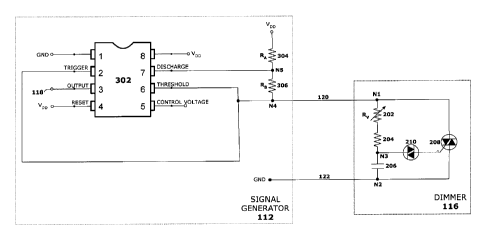
Figure 3 is a circuit diagram of the signal generator 112, also referred to as
the signal
generation circuit 112, and the dimmer 116 according to a first embodiment of
the
present invention. As shown in Figure 3, the signal generator 112 comprises a
component 302, a first resistor 304 (RA) and a second resistor 306 (RB). The
component 302 of Figure 3, according to some embodiments of the present
invention,
comprises a 555 timer integrated circuit such as ICM7555CD/01 manufactured by
NXP Semiconductor of Eindhoven, The Netherlands. It should be understood that
CA 02799658 2012-11-13
WO 2011/140631
PCT/CA2011/000524
other components with similar functionality could be utilized to implement the
present invention and the functionality of the component 302 may be
implemented by
discreet components, software and/or firmware rather than a single integrated
circuit.
As shown, the component 302 comprises eight terminals (numbered 1-8).
Terminals
1 and 8 are inputs for reference ground GND and DC supply voltage VDD
respectively. Reference ground GND and the DC supply voltage VDD are supplied
directly from the AC/DC convertor 114 in the embodiment of Figure 1B and are
supplied via DC supply/ground lines 124 in the embodiment of Figure 1C. In the
embodiment of Figure 3, terminal 4 of the component 302 is a reset terminal
and is set
to the supply voltage VDD while terminal 5 is a control voltage terminal that
may or
may not be utilized to adjust voltage thresholds for switching as will be
described
herein below. Terminals 2, 3, 6 and 7 of the component 302 comprise a trigger
terminal, an output terminal, a threshold terminal and a discharge terminal
respectively.
The dimmer 116, in this embodiment, comprises the TRIAC dimmer 200 of Figure 2
and like components are numbered with the same references. The dimmer 116 is
coupled to the signal generator 112 at nodes N1 and N2 via lines 120 and 122
respectively. In certain embodiments, node Ni may be referred to as a
connection
node. Line 120 is coupled to a node N4 described below and line 122 is coupled
to
the reference ground GND within the signal generator 112 or may otherwise be
coupled to the reference ground GND that the signal generator 112 is
utilizing. In an
alternative embodiment, line 122 may be coupled to the AC/DC convertor 114 in
order to receive the reference ground GND. A capacitor with a high capacitance
or an
Electro-Static Discharge (ESD) blocker could further be coupled to line 120.
In the embodiment of Figure 3, the first resistor 304 (RA) is coupled in
series with the
second resistor 306 (RB) between the supply voltage VDD and the node N4, node
N4
being coupled to the node N1 within the dimmer 116 via line 120. The trigger
terminal (terminal 2) and the threshold terminal (terminal 6) of the component
302 are
coupled together and further coupled to the node N4 while the discharge
terminal
(terminal 7) of the time component 302 is coupled to a node N5 defined between
the
first and second resistors 304, 306.
16
CA 02799658 2012-11-13
WO 2011/140631
PCT/CA2011/000524
With a standard DC supply voltage VDD (for example: 3 or 5V), the voltage at
node
N3 within the dimmer 116 will never be sufficient to turn on the DIAC 210 or
the
TRIAC 208. In particular, the voltage at node N3 will always be below the
breakdown voltage for the DIAC 210 and the voltage at the gate electrode of
the
TRIAC 208 will never reach the trigger voltage for the TRIAC 208. A breakdown
voltage for a DIAC 210 can be approximately 25V and a trigger voltage for a
TRIAC
208 within a TRIAC dimmer may similarly be approximately 25V. Although the
actual supply voltages may be different in a variety of embodiments of the
present
invention, the voltages applied to the DIAC and/or TRIAC within the dimmer 116
according to embodiments of the present invention are not sufficient to turn
the
components on.
Hence, in analyzing the circuit of Figure 3, the DIAC 210 and the TRIAC 208
can be
assumed to be open circuits at all times. The use of the dimmer 116 in the
circuit of
Figure 3 is not to modify an AC sinusoid as it is normally used, but instead
to allow
for the potentiometer 202 and the capacitor 206 to be included within an
overall
oscillation circuit that includes the component 302 and the first and second
resistors
304, 306. As will be described in detail, an oscillation signal with an
adjustable
frequency can be generated at the output terminal (terminal 3) of the
component 302
using the circuit of Figure 3, the oscillation signal having a frequency (and
period)
dictated in part by the resistance set at the potentiometer 202. It is noted
that the
resistance of the potentiometer 202 cannot easily be measured directly with an
ohmmeter external to the dimmer 116 since the potentiometer 202 is embedded in
series with the capacitor 206.
The circuit of Figure 3 is designed to enable the component 302 to operate
within an
astable vibrator oscillation mode. The discharge terminal (terminal 7) of the
component 302 has two states depending upon the voltage on the trigger and
threshold terminals (terminals 2 & 6), node N4 within Figure 3. In a first
state, when
the voltage on node N4 becomes one third of the supply voltage VDD or less,
the
discharge terminal (terminal 7) becomes an open circuit. In a second state,
when the
voltage on node N4 becomes two thirds of the supply voltage VDD or greater,
the
discharge terminal (terminal 7) becomes coupled to the reference ground GND.
This
17
CA 02799658 2012-11-13
WO 2011/140631
PCT/CA2011/000524
back and forth transition from the reference ground GND and an open circuit
within
the discharge terminal (terminal 7) allows the capacitor 206 within the dimmer
116 to
charge and discharge at a rate dictated by the resistance of the first and
second
resistors 304, 306 and the potentiometer 202. When the discharge terminal
(terminal
7) is an open circuit, the capacitor 206 will charge and the voltage at node
N4 will
increase based upon the voltage divider created with the combined resistance
of
resistors 304, 306 and combined resistance of the potentiometer 202 and the
resistor
204. When the discharge terminal (terminal 7) is coupled to the reference
ground
GND, the capacitor will discharge and the voltage at node N4 will decrease
based
upon the voltage divider created with the resistance of the second resistor
306 and
combined resistance of the potentiometer 202 and the resistor 204.
In the first state:
V, =V, +(Võ R ¨V,) v
Rv +RA+ R,
where V4 is the voltage on node N4; VDD is the supply voltage; Vc is the
voltage on
node N3; and RA, RB and Rv are the resistances on resistor 304, resistor 306
and
potentiometer 202 respectively. In this equation and the equation for the
second state,
the resistance of resistor 204 within the dimmer 116 is ignored for simplicity
since it
is generally relatively small compared to the resistance on the potentiometer
202.
In the first state, the voltage at node N3 (Vc) will increase as the capacitor
206
charges, thus increasing the voltage at node N4 (V4). Once the voltage at the
node N4
(V4) increases to two thirds of the supply voltage VDD (or another threshold
as could
be set), the discharge terminal (terminal 7) within the component 302 switches
and is
coupled to the reference ground GND (the second state).
In the second state:
r
R \
v
V4 = Vc
\RV + RB )
In the second state, the voltage at node N3 (Vc) will decrease as the
capacitor 206
discharges, thus decreasing the voltage at node N4 (V4). Once the voltage at
the node
N4 (V4) decreases to one third of the supply voltage VDD (or another threshold
as
18
CA 02799658 2012-11-13
WO 2011/140631 PCT/CA2011/000524
1 lA.10-U 17
could be set), the discharge terminal (terminal 7) within the component 302
switches
and is open circuited (the first state). In some embodiments, the threshold
voltage
levels on node N4 that trigger the switch from the first state to the second
state and
back can be adjusted by adjusting a voltage applied to the control voltage
terminal
(terminal 5) on the component 302 in Figure 3.
The output terminal (terminal 3) within the timing component 302 outputs the
output
signal 118 which is a representation of the switching of the discharge
terminal
(terminal 7) within the component 302 between the first and second states.
When the
discharge terminal is in the first state, the output signal 118 is a high
voltage. When
the discharge terminal is in the second state, the output signal 118 is a low
voltage.
Therefore, as the discharge terminal switches between the first and second
states, the
output signal 118 becomes an oscillation signal with an output frequency set
by the
ratio of the resistances RA, Rs, R.
One can calculate the frequency of the output signal as it relates to the
resistances RA,
RB, R. In the specific example implementation of Figure 3, while ignoring the
resistor 204, the time Tc required for the node N4 to charge to two thirds of
the supply
voltage VDD and the time TD required for the node N4 to discharge to one third
of the
supply voltage VDD are defined by the following equations:
\ (1-X \ (y\
Tc = C(R, + RH+ Ri, )1n _______________ T, =C(RB+ k )1n ¨
where:
2
X = R v ; Y = 1 + Rv and C is the capacitance of capacitor
206.
3 OA + R, ) 3 3R,
Therefore, the total time to charge and discharge can be represented by:
(1¨ ________________________ X ) t (Y )
T, +Tõ =C(RA+RB+Rv )1n + CkR, + Rv )1n ¨
1¨Y X
1
and the frequency of the output signal 118 can be calculated as: F= .
T, +T,
In order for the architecture of Figure 3 to operate properly, the values of
the
resistances RA, RB, RV must follow a particular relationship to ensure that
the node N4
19
CA 02799658 2012-11-13
WO 2011/140631
PCT/CA2011/000524
does not instantly change to less than one third of the supply voltage VDD
when the
circuit switches from the first state to the second state. The relationship
is:
<R,(R, +R,)
RA +2/?,
If the dimmer 116 is an off-the-shelf TRIAC dimmer, the range of resistance
within
the potentiometer 202 will be difficult to modify. Therefore, when designing
the
circuit of Figure 3, the selection of the resistances RA, RB for resistors
304,306 should
be done to maintain the above relationship for the various potential range of
Rv. In
one particular example, in which the potentiometer has a range of 31(.0 to
60k1, the
resistances RA, RB can both have values of 100k. This relationship can also be
adjusted by applying a voltage to the control voltage terminal (terminal 5)
within the
component 302 and therefore changing the threshold voltages at which the
component
302 switches from the first state to the second state and vice versa. When
embodiments of the invention employing an impedance matching element, such as
the
embodiment illustrated in Figure 10, are used the impact of the impedance
matching
element must also be accounted to ensure similar operation.
In the embodiment of the present invention of Figure 3, the resistors 304,306
are fixed
resistors while the potentiometer 202 has a variable resistance. As the
resistance on
the potentiometer 202 is changed by a user of the dimmer 116, the frequency
(and
period) of the output signal 118 will change in response. The output signal
118, as
depicted in Figure 1B and 1C, can be received by the lighting controller 110.
The
lighting controller 110, according to embodiments of the present invention,
can detect
the frequency of the output signal 118 or data related to the frequency (i.e.
the period).
For example, in some embodiments, the lighting controller 110 can measure the
time
between changes from high to low or low to high in the output signal 118. In
other
embodiments, the duration of a high state, low state or total duty cycle may
be
measured. In some embodiments, the lighting controller 118 could measure the
duration period of multiple cycles of high and/or low states to achieve
additional
accuracy and granularity of the setting of the potentiometer 202 within the
dimmer
116. The lighting controller 118, using the data related to the frequency of
the output
signal 118, can generate information related to the setting of the
potentiometer 202
within the dimmer 116, hereinafter referred to as dimmer information. The
period as
CA 02799658 2012-11-13
WO 2011/140631
PCT/CA2011/000524
used herein, should be construed broadly to include data related to the period
including fractions and multiples of the period and generally include data
related to
the frequency or period.
The dimmer information may be generated in a number of ways. In some
embodiments, the lighting controller 110 can use a calibration table to
determine
which of the data related to the frequency of the output signal 118
corresponds to
what corresponding dimmer information. In other cases, the lighting controller
110
may utilize a formula to generate dimmer information associated with a range
for the
data related to the frequency of the output signal 118. Other techniques for
converting the data related to the frequency of the output signal 118 to the
dimmer
information should be understood and the actual method used should not limit
the
scope of the present invention.
The lighting controller 110 can utilize the dimmer information to control an
aspect of
the lighting devices 108. In some embodiments, the lighting controller 110 can
use
the dimmer information to generate an intensity level signal to manage the
intensity of
the lighting devices 108. The intensity level signal may take a number of
forms. In
the case that the lighting devices 108 are LEDs, the intensity level signal
may
comprise a PWM signal that selectively turns on/off the LEDs for a particular
amount
of time within a duty cycle. In other cases, the intensity level signal may be
used to
adjust the current flow through the lighting devices 108. In yet other
embodiments,
the intensity level signal may be used to adjust the power to the lighting
devices 108
in other manners. For example, in the case that the lighting devices 108 are
AC
devices such as incandescent, halogen or fluorescent devices, the intensity
level signal
may adjust an AC signal being applied to the lighting devices 108.
In other embodiments, the lighting controller 110 may use the dimmer
information to
control other aspects of the lighting devices, such as the color and/or color
temperature of the lighting devices 108. For example, in the case of the
lighting
devices 108 comprising LEDs, the lighting controller 110 may turn on/off a
select set
of the LEDs for a particular time period within a duty cycle in response to
the dimmer
information in order to generate a particular light spectrum in the light
output from the
lighting apparatus 102. In some particular case, if the dimmer information
indicates
21
CA 02799658 2012-11-13
WO 2011/140631
PCT/CA2011/000524
that the lighting apparatus 102 should emit more of a red spectrum, the
lighting
controller 110 may turn on additional red LEDs or turn on a set of red LEDs
for a
longer period of time during the duty cycle. It should be understood that, in
a
scenario with various sets of LEDs of different colors and/or color
temperatures, by
adjusting which sets of LEDs are turned on and for how long each set of LEDs
are
turned on, the lighting controller 110 can change the color and/or color
temperature of
the resulting light output from the lighting apparatus 102. In other
embodiments, the
lighting controller may adjust the current flow through a plurality of sets of
LEDs in
order to adjust the resulting spectrum of the light output. As the current
level is
increased to a particular set of LEDs, the luminance of those LEDs will
typically
increase, assuming that it does not exceed the maximum allowable current.
Similarly,
as the current level is decreased to a particular set of LEDs, the luminance
of those
LEDs will typically decrease.
It should be understood that the above description of the lighting controller
110
utilizing the dimmer information should not limit the scope of the present
invention.
In some embodiments, the lighting controller 110 does not convert the data
related to
the frequency of the output signal 118 to dimmer information but instead
directly
interprets it into one or more signals that can be used to control the
lighting devices.
For example, in some embodiments, the lighting controller 110 may correlate
particular data related to the frequency of the output signal 118, for
example, the
period of the output signal 118, into particular intensity level signals
and/or signals
that can be used to control the color and/or color temperature of the lighting
apparatus
102.
It should be understood that the above description related to Figure 3 is
directed to a
particular design of the dimmer 116 and the above defined equations would
change
depending upon the specific circuits within the dimmer 116. In particular, an
alternative design for the dimmer 116 would change the calculation of the
frequency
for the output signal 118 and would also change the required relationship with
the
values of the resistors 304,306. In some cases, the circuit within the signal
generator
112 would need to be adjusted to allow for the modified design for the dimmer
116.
22
CA 02799658 2012-11-13
WO 2011/140631
PCT/CA2011/000524
In some embodiments, the lighting controller 110 can detect the minimum and
maximum frequencies that the output signal 118 can be within. This can be
accomplished by having a user of the dimmer 116 adjust the potentiometer 202
from
first and second extreme levels. By detecting data related to the frequency of
the
output signal 118 at the minimum and maximum levels, the lighting controller
110
can then utilize this data to establish a range of setting for controlling the
lighting
devices 108. For example, in one case, the lighting controller 110 could set a
linear
correlation between the minimum and maximum settings and adjust an aspect of
the
lighting devices 108 linearly depending upon the data related to the frequency
of the
output signal 118 as it relates to the maximum and minimum levels. Other non-
linear
relationships could also be used. Such a calibration procedure could be
communicated to an end user of the lighting apparatus 102 and/or control
apparatus
104 by way of a diagram or written instructions to connect the dimmer, enable
the
lighting apparatus 102 and then adjust the dial within the dimmer to each of
its
extremes slowly enough for the lighting controller 110 to capture the correct
limits.
Additional details of particular embodiments or methods that may be used to
calibrate
the lighting controller 110 to a particular dimmer 116 are described below
with
reference to Figures 8 and 9. These calibrations procedures may allow the
lighting
controller 110 to be used effectively with a variety of dimmers having
different
properties.
One example alternative dimmer design that is within a 6621-W dimmer
manufactured by Leviton Manufacturing Corporation of Melville, New York,
U.S.A.
is depicted in Figure 4. The design illustrated in Figure 4 eliminates the
TRIAC and
DIAC circuit for simplicity since the operation of the present invention
ensures that
these components are not relevant as both components remain off. As shown, a
potentiometer 402 is coupled between the line 120 and a node N6 while a first
resistor
404 is coupled between the line 120 and a node N7. A second resistor 406 is
coupled
between nodes N6 and N7. Line 122 is coupled to first and second capacitors
408,410 which are further coupled to the nodes N6 and N7 respectively. There
is also
an additional capacitor 412 coupled between the line 120 and the line 122.
In one particular implementation, the values of the linear components within
the
dimmer of Figure 4 are: potentiometer 402 of 6 to 1541a first resistor 404 of
92kCI;
23
CA 02799658 2012-11-13
WO 2011/140631
PCT/CA2011/000524
second resistor 406 of 390k12; first capacitor 408 of 68nF; second capacitor
410 of
47nF; and additional capacitor 412 of 100nF. In this particular configuration,
it has
been tested that when the dimmer of Figure 4 is implemented as dimmer 116
within a
circuit similar to Figure 3, the resistors 304,306 can both be a value of
100k. In this
set-up, the frequency of the output signal 118 adjusts between approximately
20 to
30Hz.
Although the above description includes off-the-shelf TRIAC dimmers within the
control apparatus of the present invention, it should be understood that
alternative
circuitry could be generated that does not use an off-the-shelf TRIAC dimmer
while
still gaining at least some of the benefits of the present invention. Figures
5A and 5B
are circuit diagrams of lighting control apparatus 104 according to two
particular
alternative embodiments of the present invention that do not use off-the-shelf
TRIAC
dimmers.
As depicted, the lighting control apparatus of Figure 5A is similar to the
circuit of
Figure 3 with like components being marked with the same references. Instead
of the
dimmer 116 within Figure 3, the circuit of Figure 5A has a potentiometer 502
coupled
in series with a capacitor 504 between node N4 and the reference ground GND.
This
circuit is effectively the component equivalent of Figure 3 with the resistor
204,
TRIAC 208 and DIAC 210 removed and may be implemented directly in certain
embodiments of the invention in place of a dimmer having TRIAC circuitry.
Since
the circuit is equivalent, the operation of the circuit is equivalent and the
formula for
the frequency of the output signal 118 is the same as indicated above for
Figure 3.
The lighting control apparatus of Figure 5B includes the component 302 which
is
used similar in function to the circuit of Figure 3. As depicted, the circuit
of Figure
5B further comprises a resistor 506 coupled in series with a potentiometer 508
and a
capacitor 510 between the supply voltage VDD and the reference ground GND. As
shown, a node N8 between the potentiometer 508 and the capacitor 510 is
coupled to
the threshold terminal (terminal 6) and the trigger terminal (terminal 2) of
the
component. Further, a node N9 between the resistor 506 and the potentiometer
508 is
coupled to the discharge terminal (terminal 7) of the component 302.
24
CA 02799658 2012-11-13
WO 2011/140631
PCT/CA2011/000524
In the configuration of Figure 5B, the component 302 generates an output
signal 118
similar to the output signal described above with reference to Figure 3. In
particular,
the output signal 118 can be used in a similar manner by the lighting
controller 110
with the frequency of the output signal 118 being dependent at least partially
on the
resistance of the potentiometer 508, the potentiometer 508 being adjusted by a
user of
the control apparatus. The formula for the frequency F of the output signal in
this
particular configuration is:
F= 1.38
(RA, +2R,, )C
where RAI is the resistance of resistor 506, Rv 1 is the resistance of the
potentiometer
508 and C is the capacitance of capacitor 510.
It should be understood that the control apparatus of Figures 5A and 5B are
only two
particular examples of implementations of the present invention not utilizing
an off-
the-shelf TRIAC dimmer. Other circuits that can utilize a potentiometer to
allow for
the adjusting of a frequency for an output signal can be used. For instance,
the
component equivalent of well-known TRIAC dimmers with the TRIAC and DIAC
components removed could be used along with a component similar to that of
component 302 to generate an output signal of a frequency that is dependent at
least
partially on the setting of a potentiometer.
It should further be understood that the use of the component 302 within the
circuits
of Figures 3, 5A and 5B could be replaced with discrete components that
operate in a
similar fashion. For example, one skilled in the art would understand
equivalent
circuits to replicate the functionality of a 555 Timer. These equivalent
circuits for the
time component could be used to create a functionally similar circuit to the
circuits of
Figures 3, 5A and 5B.
In the system architectures depicted in Figures 1B and 1C, the lighting
apparatus 102
and the control apparatus 104 are coupled together by fixed DC lines (120,122
in the
case of Figure 1B and 118,124 in the case of Figure 1C). It should be
understood that
in alternative embodiments, the lighting apparatus 102 and the control
apparatus 104
may communicate wirelessly as will be described herein below with reference to
CA 02799658 2012-11-13
WO 2011/140631
PCT/CA2011/000524
Figure 6A or may communicate over AC lines as described herein below with
reference to Figure 6B.
Figure 6A is a system architecture diagram according to embodiments of the
present
invention using wireless technology for communication. The architecture of
Figure
6A is a modified version of the architecture of Figure 1C and therefore like
components are marked with the same references. Within Figure 6A, the control
apparatus 104 has a separate AC mains input 602 and does not receive DC power
through DC power/ground lines 124. Instead, the control apparatus 104 of
Figure 6A
comprises an AC/DC convertor 604 which supplies DC power to the circuit
comprising the signal generator 112 and the dimmer 116. Alternatively, the AC
mains input 602 and AC/DC convertor 604 could be replaced with a separate DC
power source such as a battery or a solar array device. The control apparatus
104 of
Figure 6A further comprises a wireless transmitter 606 that receives DC power
from
the AC/DC converter 602 (or the separate DC power source) and the output
signal
118 from the signal generator 112.
Within Figure 6A, the lighting apparatus comprises the AC/DC convertor 114,
the
lighting controller 110 and the lighting devices 108 similar to that depicted
in Figure
1C but the lighting apparatus further comprises a wireless receiver 610 that
receives
DC power from the AC/DC convertor 114.
In operation, the wireless transmitter receives the output signal 118 from the
signal
generator 112 and transmits a wireless signal 610 to the wireless receiver
608, the
wireless signal 610 incorporating information related to the output signal
118. In one
embodiment, the wireless transmitter 606 is an FSK transmitter that modulates
a
higher frequency pilot signal using the relatively low frequency output signal
118. In
other embodiments, the wireless transmitter 606 may regenerate a new signal
within a
wireless standard such as SigBe, Bluetooth, WiFi, WiMax, CDMA, GSM, etc. that
conveys information related to the output signal 118 such as data related to
its
frequency. The wireless receiver 608 in operation receives the wireless signal
610
and may modify the signal. For instance, the wireless receiver 608 may
demodulate
the output signal 118 and effectively regenerate it as signal 612 for
forwarding to the
lighting controller 110. In other embodiments, the wireless receiver 608 may
interpret
26
CA 02799658 2012-11-13
WO 2011/140631
PCT/CA2011/000524
information within the wireless signal to generate the signal 612 for
forwarding to the
lighting controller 110. In yet other embodiments, the wireless receiver 608
may
remove overhead attached by the wireless transmitter 606 and forward the
content or
a representation thereof as signal 612 to the lighting controller 110. In all
cases
within the architecture of Figure 6A, the wireless transmitter 606 and the
wireless
receiver 608 work together to wirelessly communicate information within the
output
signal 118 to the lighting controller 110. It should be understood that one
skilled in
the art may contemplate other implementations for communicating information
from
the output signal 118 to the lighting controller 110.
Figure 6B is a system architecture diagram according to embodiments of the
present
invention using AC wire coupling technology for communication. The
architecture of
Figure 6B is a modified version of the architecture of Figure 1C and therefore
like
components are marked with the same references. Within Figure 6B, the control
apparatus 104 has an AC mains input 614 coupled to an AC/DC convertor 616
which
supplies DC power to the circuit comprising the signal generator 112 and the
dimmer
116. The control apparatus of Figure 6B further comprises a signal coupler 618
that is
powered by the DC output of the AC/DC convertor 616 and receives the output
signal
118 from the signal generator 112 as well as the AC supply from the AC input
614.
The signal coupler 618 uses power line carrier (PLC) or broadband over power
line
(BPL) technology to modulate the output signal 118 onto the AC supply such
that an
AC line 620 coupled between the control apparatus 104 and the lighting
apparatus
102 has the AC supply with information associated with the output signal 118
modulated onto the AC sinusoid. In one embodiment, the signal coupler 618
comprises an FSK transmitter that modulates a higher frequency pilot signal
using the
relatively low frequency output signal 118.
Within Figure 6B, the lighting apparatus 102 comprises the lighting controller
110
and the lighting devices 108 of Figure 1C but, instead of the AC/DC convertor
114,
the lighting apparatus 102 further comprises a signal decoupler 622 and an
AC/DC
convertor 624. The signal decoupler 622 is coupled to the AC line 620 and
demodulates the signal modulated onto the AC sinusoid. The resulting AC signal
is
converted by the AC/DC convertor 624 into a DC supply that powers the lighting
controller 110, the lighting devices 108 and the signal decoupler 622. The
signal
27
CA 02799658 2012-11-13
WO 2011/140631
PCT/CA2011/000524
decoupler 624 transmits a signal 626 that resulted from the demodulation to
the
lighting controller 110. The signal 626 may be a regeneration of the output
signal 118
or may be a signal that incorporates information related to the frequency of
the output
signal 118.
In both the implementations of Figures 6A and 6B, a signal representative of
the
output signal 118 or that incorporates information related to the output
signal 118 is
received by the lighting controller 110. In these cases, the lighting
controller 110 can
control the lighting devices 108 in a similar manner as described above. In
particular,
the lighting controller can control an aspect of the light output from the
lighting
apparatus 102 by controlling the lighting devices 108 in response to the
signals
received indirectly from the signal generator 112.
Figure 7 is a circuit diagram for powering a control apparatus according to
one
particular example implementation of the present invention. In specific
implementations of the present invention, the component 302 may need to be
powered
from a DC source but with only an AC source available. This could occur in the
embodiments depicted in Figures 6A and 6B as well as the embodiment depicted
in
Figure 1C if the DC power/ground lines 124 were removed. The circuit of Figure
7
depicts one particular implementation that could be used to power the
component 302
from an AC supply. As shown, the circuit of Figure 7 comprises the component
302
being powered from an AC supply 704. The AC supply 704 is coupled to a voltage
divider 706 which is subsequently coupled to a rectifier 708. The outputs from
the
rectifier 708 are the voltage supply VDD and the reference ground GND. As
shown, a
capacitor 710 and a zenor diode 712 are coupled between the outputs of the
rectifier.
It should be understood that many other well-known techniques for AC/DC
conversion can be used for this situation and the implementation of Figure 7
is only
one example of a bridge rectifier.
One example of a calibration procedure that may be used by lighting controller
110 to
determine the maximum and minimum periods of the output signal 118 when used
with a particular dimmer 116, as noted above, is illustrated in further detail
in Figure
8. The dimmer 116 may have an interface that may have a value that is
representative
of the state of the interface and may change as the interface of the dimmer
116 is
28
CA 02799658 2012-11-13
WO 2011/140631
PCT/CA2011/000524
adjusted. For example, in certain embodiments, the value of the interface may
be
considered to be the impedance of a variable impedance, such as the variable
resistor
202 included in the TRIAC dimmer, depicted in Figure 2, or an alternative
dimmer
having a variable impedance in series with a capacitor. Such a calibration
procedure
may be important to provide a full range of adjustment of an aspect of light
output
desired to be controlled with the dimmer 116, because the maximum and minimum
periods of the output signal 118 may vary depending on the properties (e.g.
resistance
and capacitance) of the particular dimmer 116 coupled to the signal generator
112
(also referred to as the signal generation circuit).
Written instructions may be provided to users to allow users to interpret
instructions
from the lighting controller 110 and adjust the interface of the dimmer 116
appropriately. When the lighting controller 110 is in a programming mode, the
lighting controller 110 may instruct the user to set the interface of the
dimmer 116 to a
first extreme value at step 150. The lighting controller 110 may enter a
programming
mode when initialized, or first turned on, or when it is desired to change
certain
parameters of the lighting controller 110. For example, the lighting
controller 110
may cause the lighting devices 108 (light radiating element) to flash or blink
a set
number of times to instruct the user to set the value of the interface to a
first extreme
value, for example, the minimum value. The lighting controller may then
determine
the period of the output signal 118 at step 152 and store the period, for
example, the
minimum period in memory. As noted above, the period as used herein should be
understood to be a duration or other data related to the frequency of a
signal, and may
include, for example, a half period, for example, the time it takes a signal
to transition
from high to low and vice versa and multiples of the period. In order to
facilitate an
accurate measurement of the period at the first extreme value, the minimum
period in
this example, the lighting controller 110 may wait a certain period of time to
ensure a
steady state is reached and/or average a number of samples in an attempt to
reduce the
effects of possible noise. The lighting controller 110 may then instruct the
user to set
the value of the interface to a second extreme value, for example, the maximum
value
at step 154. As noted above, instructing the user to set the interface to a
second
extreme value may be communicated by flashing the lighting devices 108 a
predetermined number of times or using another method. The lighting controller
110
may then determine the period of the output signal 118 at the second extreme
value,
29
CA 02799658 2012-11-13
WO 2011/140631
PCT/CA2011/000524
which in this example would be the maximum period of the output signal 118 and
store the maximum value in memory at step 156.
After the periods have been determined at the first and second extremes, the
user may
adjust the interface of the dimmer 116 to a desired value. The lighting
controller 110
may determine the period of the output signal 118 associated with the present
value of
the interface of the dimmer 116 at step 158. The lighting controller 110 may
then
control an aspect of light output from the lighting devices 108 based on the
period
relative to the periods at the first and second extreme values of the
interface of the
dimmer 116 (e.g. the minimum and maximum periods) at step 160. For example,
lighting controller 110 may be configured so that the perceived light output
(i.e. the
output perceived by the human eye) varies approximately linearly as the value
of the
interface is adjusted from a minimum to a maximum value. Lighting controller
110
may need to convert such an approximately linear relationship to an
approximately
exponential relationship, for example, to account for lighting devices 108,
such as
LEDs, that have a non-linear light output (i.e. a non-linear IV curve of a
LED).
Lighting controller 110 may also continuously monitor and determine the period
of
the output signal 118 to adjust the light output from the lighting devices 108
responsive to changes to the interface of the dimmer 116 in a similar manner.
Alternatively, the user may cause the lighting controller 110 to enter a
programming
mode in certain embodiments, for example, by communicating a command via a
remote control. The lighting controller 110 may alternatively be operable to
enter a
programming mode upon initialization. In a programming mode, the user may set
the
interface of the dimmer to the maximum and minimum extremes within a
predetermined amount of time and the maximum and minimum periods of the output
signal 118 may be captured and stored by the lighting controller 110. Written
instructions may be provided to instruct the user to set the maximum and
minimum
periods within a predetermined amount of time and to leave the interface of
the
dimmer at the maximum and minimum extremes for a certain amount of time to
ensure an accurate reading. An aspect of the light output from the lighting
devices 108
may then be controlled based on the value of the output signal 118 relative to
the
maximum and minimum periods of the output signal 118 as described above.
CA 02799658 2012-11-13
WO 2011/140631
PCT/CA2011/000524
Figure 9 illustrates an alternative calibration procedure that may allow
lighting
controller 110 to control the light output from lighting devices 108 when used
with a
particular dimmer 116 having a particular range of impedance values that may
be
adjusted by changing the value of an interface. The dimmer 116 may have an
interface that may have a value representative of the state of the interface
of the
dimmer, for example, the impedance of a variable impedance that may be
adjusted by
the interface as described above. In contrast to the calibration procedure
described
with respect to Figure 8, the calibration procedure illustrated in Figure 9
does not
require the user to undertake a series of steps in a programming mode, or upon
initialization, of the lighting controller 110 and may be referred to as an
adaptive or
automatic calibration procedure.
When the lighting controller 110 is in a programming mode, for example, when
initialized or turned on, the interface of the dimmer 116 may have an initial
value. It
should be understood that when sampling periods, the samples may be filtered
for
noise by, for example, eliminating the 2 greatest outliers among 8 running
samples
leading to the present sample and using the average of the 6 non-outliers as
the
"sample". Additionally, when sampling for the minimum and maximum, additional
care can be taken to ensure that at least 256 (or some other large number) of
samples
occurred within 1 or 2 units of the maximum or minimum being updated, since
the
normal use of a dimmer is to leave it alone once the user has adjusted it to
the
appropriate level. The lighting controller 110 may determine the initial
period of the
output signal 118 after a delay to ensure that a steady state has been reached
and store
the value of the period in memory at step 250. The lighting controller 110 may
then
establish a maximum period of the output signal 118 at step 252. The maximum
period should be chosen to be in close proximity to the initial period upon
initialization. For example, the maximum period could be set to be the initial
period,
or another period in close proximity to the initial period, such as the
initial period plus
1. Alternative methods to establish an initial value of the maximum period may
also
be used in certain implementations. Similarly, the lighting controller 110 may
establish an initial value for a minimum period of the output signal 118 and
store the
minimum period in memory at step 254. The initial value of the minimum period
may
also be chosen to be in close proximity to the initial period, for example,
the initial
value of the minimum period could be chosen to be the initial period minus 1.
Other
31
CA 02799658 2012-11-13
WO 2011/140631
PCT/CA2011/000524
initial values for the minimum period may also be chosen without departing
from the
scope of the invention. Steps 250, 252, and 254 may be considered to be part
of the
initialization procedure of the lighting controller 110 and may only be
performed
when the lighting controller 110 is first turned on or in a programming mode.
During continued or ongoing operation, the lighting controller 110 may
determine the
period of the output signal 118 at step 256 and be operable to detect changes
in the
period of the output signal 118 as the value of the interface of the dimmer is
changed.
If the period of the output signal 118 is greater than the maximum value of
the period
stored in memory the maximum value may be set to be the period of the output
signal
118 and the updated maximum value may be stored in memory at step 258.
Analogously, if the period of the output signal 118 is less than the minimum
value of
the period stored in memory the minimum value may be set to be the period of
the
output signal 118 and the updated minimum value may be stored in memory at
step
260. The lighting controller 110 may then control an aspect of the light
output from
lighting devices 108 based on the period of the output signal (value of the
interface of
the dimmer) relative to the maximum and minimum values of the period at step
262.
For example, an aspect of the light output may be controlled based on the
percentage
that the period is between the minimum and maximum values. The minimum and
maximum values of the period may also be considered to be a first and second
extreme value of the interface as used hereinafter. To achieve a percentage
value of an
aspect of the light output to be controlled the following representative
formula may be
used:
(Period ¨ MinimumPeriod)
%Aspect =
(MaximumPeriod ¨ MinimumPeriod)
Alternatively, other methods to control an aspect of the light output, such as
the
luminosity may also be used without departing from the scope of the invention.
The
lighting controller 110 may then proceed to determine the period of the output
signal
118 to determine if the period has changed responsive to a change in the value
of the
interface at step 256 and repeat the steps 256, 258, 260, and 262 in a loop
during
continued operation.
32
CA 02799658 2012-11-13
WO 2011/140631
PCT/CA2011/000524
Other embodiments of the invention may not utilize a calibration procedure or
adaptive algorithm to account for the variation between various types of
dimmers,
including different implementations of TRIAC dimmers that may have a different
range of resistance or impedance values. Instead, these embodiments may be
designed
to be suitable for use with a particular model of a dimmer having known
properties.
For example, one embodiment of the invention may be designed to be used with a
particular TRIAC dimmer having known properties so that the minimum and
maximum periods, or more generally the value of the interface, at the first
and second
extreme values of the interface of the dimmer are known and the lighting
controller
110 may control an aspect of the light output based on the period of the
output signal
118 relative to the known minimum and maximum periods.
These embodiments may be suitable for use with a low cost lighting controller
110
that may have limited functionality, for example, the Lutron Skylark model
number 5-
600H-WH-CSA. For example, certain lighting controllers 110 may have limited
memory resources such that a minimum and maximum value of the interface of the
dimmer 116 or period of the output signal 118 of the signal generation circuit
112
cannot be stored dynamically, but rather must be programmed into ROM as part
of
the manufacture of the lighting controller 110. In one embodiment, the minimum
and
maximum periods of the output signal 118 for a particular dimmer 116 may be
programmed during the manufacture of the lighting controller 110 so that the
period
of the output signal 118 may be properly interpreted by the lighting
controller 110,
when used with the particular dimmer 116, to control an aspect of the light
output
from the lighting devices 118 based at least in part on the period of the
output signal,
or the value of the interface of the dimmer 116, relative to the maximum and
minimum values of the period of the output signal 118 or the maximum and
minimum
values of the interface.
In another embodiment of the invention illustrated in Figure 10, a lighting
controller
110 may be matched to a particular dimmer even though the lighting controller
110
has a predetermined maximum and minimum period that was not specifically
calibrated for use with the particular dimmer. The signal generation circuit
112 (signal
generator) and dimmer 116 may have the same functionality as described with
reference to Figure 3. This embodiment may also include an impedance matching
33
CA 02799658 2012-11-13
WO 2011/140631
PCT/CA2011/000524
circuit 315 so that the period of the output signal 118 when the signal
generation
circuit 112 is coupled to the dimmer 116 has a minimum and maximum period that
is
in close proximity to the predetermined minimum and maximum values that are
programmed into the lighting controller 110. In this manner, the lighting
controller
110 may control an aspect of the light output, such as the luminosity
(intensity) of the
lighting devices 108, based on the period of the output signal 118 relative to
the
maximum and minimum periods.
The impedance matching circuit 315 may be comprised of a variable resistor 307
connected in series with node Ni of the dimmer 116 and a variable resistor 313
connected in parallel between node Ni of the dimmer 116 and node N2. Although
adjustments to the impedance of both variable resistors 307 and 313 affect the
period
of the output signal 118, adjusting variable resistor 307 may be considered to
primarily change the absolute value of the period of the output signal 118.
Conversely, adjustments to variable resistor 313 may be considered to
primarily
change the difference between the maximum and minimum values of the period of
the
output signal 118. Alternatively, certain embodiments of the impedance
matching
circuit 315 may only include variable resistor 307 and not variable resistor
313, but
may lack the range of adjustment when compared to an impedance matching
circuit
315 having multiple variable resistors as described above. In a further
alternative,
impedance matching circuit 315 may be implemented using transresistance or
transimpedance amplifiers instead of variable resistors and may generally be
considered to be comprised of elements having variable impedances that may be
adjusted as required in the particular implementation.
Certain embodiments of lighting apparatus 102 may also include a frequency
compensation circuit 317 that may be coupled between the signal generation
circuit
112 and dimmer 116 as shown in Figure 11. The signal generator 112 and dimmer
116 may have the same functionality as previously described with reference to
Figure
3. The frequency compensation circuit 317 may comprise a resistor 309 in
series with
a capacitor 311 coupled between nodes Ni and N2 of dimmer 116. The resistor
309
may be chosen to be a large resistance, for example, 1 MCI, and the capacitor
311 may
be chosen to be, for example, 1 mF, for use with many TRIAC dimmers. Other
values
of the resistor 309 and capacitor 311 may be required for use with certain
34
CA 02799658 2012-11-13
WO 2011/140631
PCT/CA2011/000524
implementations of dimmer 116. The frequency compensation circuit 317 may act
to
prevent a runaway frequency of the output signal 118 when the signal
generation
circuit 112 is disconnected from the dimmer 116 to increase the stability of
the
lighting apparatus 102.
Figure 12 depicts another embodiment of lighting apparatus 102 that is similar
in
functionality to that previously described in Figure 1B, so like components
may be
assumed to have like functionality. In addition to the components previously
described, the embodiment in Figure 12 may include an optical coupler 111 that
may
be coupled between the lighting controller 110 and signal generator 112 and
powered
by the AC/DC converter 114. The optical coupler 111 may be comprised of a
photodiode and infrared emitter, as is known in the art, and provide isolation
between
the signal generator 112 and lighting controller 110. Additionally, the signal
generator
may be isolated electrically from the AC/DC converter by means of a second
transformer winding, or even an LED based optical power coupling system using
a
small solar panel and LED since the current required is minimal. Providing
isolation
between the signal generator 112 and lighting controller 110 may improve
performance in certain embodiments where common mode currents are present and
may impact the reliability of the lighting apparatus 102.
Another embodiment of the lighting apparatus 102 is depicted in part in Figure
13A.
Generally, this embodiment may be considered to use an astable multivibrator
to
implement a signal generation circuit 805 in place of the circuit described
previously
with reference to Figure 3. This embodiment may have a dimmer 116 coupled to a
signal generation circuit 805 that may be implemented as an astable
multivibrator,
which is well known in the art, operable to generate an output signal 807. The
output
signal 807 may have a period that is dictated at least in part by the value of
the
interface of the dimmer 116. The output signal 807 may be received by a
lighting
controller 110 that may control an aspect of the light output from the
lighting devices
108 as previously described.
The astable multivibrator used to implement one embodiment of signal
generation
circuit 805 may comprise transistors 814 and 822 that may be npn bipolar
junction
transistors (BJT). The astable multivibrator may also include resistors 808,
810, 816,
CA 02799658 2012-11-13
WO 2011/140631 PCT/CA2011/000524
and 818 and capacitors 812 and 820 that may be connected as illustrated in
Figure
13A and may have the following component values, in one particular
implementation:
Component Value
Resistor 808 500 kn
Resistor 810 1 MC2
Capacitor 812 10 nF
Resistor 816 1 MS2
_ _
Resistor 818 500 kt2
Capacitor 820 10 Nf
The lighting apparatus 102 may also be constructed using a variable voltage
signal
generation circuit 800 that is illustrated in Figures 13B-13D. For example, as
shown
in Figure 13B, a variable voltage signal generation circuit 800 may be coupled
to a
dimmer 116, which may be a TRIAC dimmer, and may have an output signal 834
that
may have a voltage that is dictated at least in part by the value of the
interface of the
dimmer 116 and may vary as the value of the interface is adjusted. The output
signal
834 may be received by a driving circuit 870 that is operable to control an
aspect of
the light output from lighting devices 108 based on the voltage of the output
signal
834. More specifically, the driving circuit 870 may operate to supply a PWM
signal to
the lighting devices 108 having a duty cycle that is dictated at least in part
by the
voltage of the output signal 834. The driving circuit 870 may be implemented
as a
lighting controller 880 as shown in Figure 13C, a monostable multivibrator 850
as
described below in greater detail with reference to Figure 14, or as a circuit
using a
555 timer operating in a monostable vibratory oscillation mode as described
below in
greater detail with reference to Figure 15B. In embodiments where the driving
circuit
870 is implemented as a lighting controller 880, a constant current signal
could be
supplied to the lighting devices 108, with the current being dictated at least
in part by
the voltage of the output signal 834. The fact that the variable voltage
signal
generation circuit 800 is operable to provide a variable voltage output may be
advantageous as it may allow the variable voltage signal generation circuit
800 to be
used with existing lighting controllers that have been designed for use with 0-
10V
dimmers currently on the market allowing TRIAC dimmers to be used in place of
0-
36
CA 02799658 2012-11-13
WO 2011/140631
PCT/CA2011/000524
10V dimmers. This may allow existing lighting systems to be more readily
modified
for use with the variable voltage signal generation circuit 800 and more
generally for
use with a TRIAC dimmer.
One particular embodiment of a variable voltage signal generation circuit 800
is
illustrated in Figure 13D. The dimmer 116 may have an interface as previously
described and may be a TRIAC dimmer, although other types of dimmers may be
used in certain embodiments. The dimmer 116 may be coupled to a resistor 802
that is
coupled to a DC power supply VDD at a power supply node 804. The output node
806
of the dimmer 116 may be coupled to a signal generation circuit 801. The
signal
generation circuit 801 may be operable to generate a periodic signal 823
having a
period that may be dictated at least in part by the value of the interface of
the dimmer
116. A voltage conversion circuit, such as the filter 803, may be coupled to
the signal
generation circuit 801 to receive the periodic signal 823 and generate an
output signal
834. The output signal 834 generated by the voltage conversion circuit, for
example,
the filter 803 may have a voltage that is dictated at least in part by the
period of the
periodic signal 823 so that the voltage of the output signal 834 is dictated
at least in
part by the value of the interface of the dimmer 116. The filter 803 may be,
for
example, a low pass filter although other types of filters may be used.
Alternatively, the voltage conversion circuit may be implemented in another
configuration that may generate an output signal having a voltage that is
dependent on
the frequency of the input signal without departing from the scope of the
invention.
For example, the voltage conversion circuit may be implemented as a
microcontroller
operable to receive the periodic signal 823 and generate an output signal 834
having a
voltage that is dictated at least in part by the value of the interface of the
dimmer 116.
Additionally, the signal generation circuit 801 shown in Figure 13D may be
implemented using a 555 timer in an astable vibratory oscillation mode,
similar to that
described with reference to Figure 3, in place of an astable multivibrator and
may be
used with either a microcontroller or filter 803 with suitable modification to
generate
an output signal 834 having a voltage that is dependent on the value of the
interface of
the dimmer 116.
37
CA 02799658 2012-11-13
WO 2011/140631
PCT/CA2011/000524
The signal generation circuit 801 may be implemented as an astable
multivibrator,
similar to that described above with reference to Figure 13A.
An embodiment of the filter 803 may have a variable resistor 824 coupled in
series to
the output of the signal generation circuit 801. The value of the variable
resistor 824
may vary depending on the particular dimmer 116 that may be coupled to the
variable
voltage signal generation circuit 800 and may be, for example, 100 ka The
variable
resistor 824 may be coupled to the base of an npn BIT 828 and a capacitor 826
that
may be coupled in parallel with the BIT 828 and coupled to ground at one
terminal.
The emitter of the BIT 828 may be coupled to ground and the collector may be
coupled to a resistor 830 and capacitor 832 connected in parallel to a DC
supply
voltage VDD. The output signal 834 may also be taken from the node common to
the
collector of BIT 828 and the resistor 830 and capacitor 832. The component
values in
one particular implementation may be as follows: capacitor 826 ¨ 0.67 nF;
resistor
830 - 100 kil; and capacitor 832¨ 1 g.
One implementation of a driving circuit 870, that does not employ a
microcontroller,
which may reduce costs, is illustrated in Figure 14. As noted above, the
driving circuit
870 may operate to generate a PWM signal to be supplied to the lighting
devices 108
having a duty cycle that may be adjusted to control an aspect of the light
output from
the lighting devices. For example, the duty cycle of the PWM signal may be
dictated
at least in part by the voltage of the output signal 834 received from a
variable voltage
signal generation circuit 800. In one embodiment, the driving circuit 870 may
include
an astable multivibrator 827 as configured in Figure 14 that is operable to
generate a
periodic signal 825. The component values used in the astable multivibrator
827 may
vary depending on the particular application, however, the component values of
a
sample implementation may be as follows:
Component Value
Resistor 809 10 Idl
Resistor 811 1 Nu/
Capacitor 813 3 nF
Resistor 817 1 MS/
38
CA 02799658 2012-11-13
WO 2011/140631
PCT/CA2011/000524
Resistor 819 10 kl2
Capacitor 821 100 pF
Alternatively, a circuit employing a 555 timer operating in an astable
vibratory
oscillation mode may be used in place of the astable multivibrator 827 in
certain
embodiments as will be described with reference to Figure 15B.
A resistor 886 may be coupled in series between the output of the astable
multivibrator 827 and an amplifer 884 with the amplifier 884 coupled to
receive the
periodic signal 825. The amplifier 884 may comprise a pnp BJT 880, with the
base of
BJT 880 being coupled to the resistor 886. The emitter of the BJT 880 may be
coupled to a resistor 888, with the resistor 888 also being coupled to a DC
power
supply VDD. The collector of BJT 880 may be coupled to the base of a npn BJT
882.
The emitter of BJT 882 may be coupled to ground and the collector may be
coupled to
a node N10. The amplifier 884 may be operable to provide isolation to the
astable
multivibrator 827 and generate an amplified version of the periodic signal
825.
The input to a monostable multivibrator 850 may also be coupled to node N10 to
receive the amplified version of the periodic signal 825. The monostable
multivibrator
850 may have a npn BJT 836 having its base coupled to node N10. The emitter of
BJT 836 may be coupled to ground and the collector may be coupled to a
resistor 838
that may be coupled to the DC power supply VDD. A resistor 842 may also be
coupled
between the collector of BJT 836 and a node N11. A resistor 840 may also be
coupled
between the DC power supply VDD and node N11. A resistor 844 may be coupled
between node N11 and ground. The base of a npn BJT 848 may be coupled to node
N11. The emitter of BJT 848 may be coupled to ground and a resistor 846 may be
coupled between the collector of BJT 848 and the DC power supply VDD. The
collector of BJT 848 may also be coupled to a capacitor 852, with the
capacitor 852
also being coupled to node N10. A driving signal 860 may be generated by the
monostable multivibrator 850 and output via a line coupled to the collector of
BJT
836. The driving signal 860 may be coupled to the lighting devices 108 to
provide a
current to provide a light output from the lighting devices 108.
39
CA 02799658 2012-11-13
WO 2011/140631
PCT/CA2011/000524
Alternatively, a circuit employing a 555 timer operating in a monostable
vibratory
oscillation mode may be operable to receive the amplified version of the
periodic
signal 825 and generate a driving signal 860 in a similar fashion to the
monostable
multivibrator 850 described above.
A variable voltage dimmer 854 may also be coupled to the driving circuit 870
at node
N10. The variable voltage dimmer 854 may also be coupled to a resistor 856
that may
be coupled to a DC power supply VDD. The variable voltage dimmer 854 may
provide
a control signal (not shown) to node N10 having a voltage that is
representative of the
value of the interface of the variable voltage dimmer 854 and varies depending
on the
value of said interface. The output signal 860 may vary depending on the
voltage of
the control signal provided to node N10 by the variable voltage dimmer 854 so
that
the driving signal 860 is dictated at least in part by the value of the
interface of the
variable voltage dimmer 854. More specifically, the driving signal 860 may be
a pulse
width modulated (PWM) signal having a duty cycle that is dependent on the
voltage
of the control signal so that an aspect of the light output from the lighting
devices, for
example, the luminosity, may be controlled by the duty cycle of the driving
signal
860.
The variable voltage dimmer 854 may be implemented as a variable voltage
signal
generation circuit 800, as described with reference to Figures 13B-13D, that
may be
configured to have the output signal 834 coupled to node N10 so that the duty
cycle of
the driving signal 860, which may be a PWM signal, is dictated at least in
part by the
voltage of the output signal 834. This particular configuration may be a low
cost
implementation that facilitates that use of a TRIAC dimmer. Alternatively, a
commercially available 0-10 y dimmer, which may be implemented as a
potentiometer and diode in series, may be used to implement a variable voltage
dimmer 854 in certain embodiments. Of course, other analogous circuits could
be
used to provide a similar functionality without departing from the scope of
the
invention and the circuit described above is merely a representative example
of a
possible implementation. For example, other possible implementations of a
variable
voltage signal generation circuit, driving circuit, etc. may be used without
departing
from the scope of the invention.
CA 02799658 2012-11-13
WO 2011/140631
PCT/CA2011/000524
Other possible embodiments of a lighting apparatus that do not employ a
lighting
controller 110 may also be used with a dimmer 116, which may be a TRIAC
dimmer,
without departing from the scope of the invention. For example, lighting
apparatus
900 illustrated in Figure 15A may be implemented using two 555 timers or
circuits
having similar functionality. The 555 timers 902 and 904 may have the same
terminal
numbering and functionality as described previously with respect to component
302,
illustrated in Figure 3. Similarly, components with element numbers previously
used
may have similar functionality to that previously described, including the
dimmer 116
and the lighting devices 108.
Lighting apparatus 900 may have a capacitor 912 coupled between a DC power
supply VDD and ground. In parallel with the capacitor 912, a resistor 906 may
be
connected in series with a variable resistor 902 between the DC power supply
VDD
and node N91. A resistor 910 may be coupled between node N91 and node N92.
A dimmer 116 may have a connection node coupled to node N92 and a line 930
coupled to ground. A 555 timer 902 may have terminal 7 (discharge) coupled to
node
N91. Terminals 4 (reset) and 8 of the 555 timer 902 may be coupled to the DC
power
supply VDD. Terminals 2 (trigger) and 6 (threshold) of the 555 timer 902 may
be
coupled to node N92 so that an indication of the value of the interface of the
dimmer
116 may be provided to the 555 timer 902. Terminal 1 of the 555 timer 902 may
be
coupled to ground and terminal 5 (control voltage) may be coupled to a
capacitor 914,
which is in turn coupled to ground. The output terminal, terminal 3, of the
555 timer
902 may be coupled to terminal 2 (trigger) of a second 555 timer, 555 timer
904.
Resistor 918 may be coupled in series with a variable resistor 920 between the
DC
power supply VDD and node N93. A capacitor 916 may be coupled between node N93
and ground. Terminals 6 (threshold) and 7 (discharge) of the 555 timer 904 may
also
be coupled to node N93. Terminals 4 (reset) and 8 of the 555 timer 904 may be
coupled to the DC power supply VDD. Terminal 1 of the 555 timer 904 may be
coupled to ground and terminal 5 (control voltage) may be coupled to a
capacitor 922,
which is in turn coupled to ground. The output terminal, terminal 3, of the
555 timer
904 may be coupled to a resistor 924, the resistor 924 may also be coupled to
the base
of a transistor 926, which may be a npn WT. The emitter of the transistor 926
may be
41
CA 02799658 2012-11-13
WO 2011/140631
PCT/CA2011/000524
coupled to ground and the collector of the transistor may be coupled to the
lighting
devices 108, which may also be coupled to the DC power supply VDD. In this
configuration, the output signal provided from 555 timer 904 may be used to
modulate the current that may flow from the DC power supply VDD through the
lighting devices 108 by modulating the current that flows through transistor
926.
More specifically, a PWM signal may be supplied to the lighting devices 108
having a
duty cycle that is dictated at least in part by the value of the dimmer 116 so
that an
aspect of the light output from the lighting devices 108 may be controlled by
adjusting
the duty cycle of the PWM signal responsive to changes to the interface of the
dimmer 116. Alternatively, other configurations including different types of
transistors may be used without departing from the scope of the invention
according
to well known principles. Generally, the component values for elements shown
in
Figure 15A should be chosen so that the 555 timer 902 operates in an astable
vibrator
oscillation mode and the 555 timer 904 operates in a monostable vibrator
oscillation
mode. More specifically, the component values for elements shown in Figure 15A
should be chosen to allow the frequency of the 555 timer 902, which may act
similarly to an astable multivibrator, to change between two values based on
the
TRIAC dimmer such that the first value is a maximum period and the second
value is
a minimum period. Similarly, components should be chosen to ensure that the
decay
time of the 555 timer 904, which may act similar to a monostable
multivibrator, is
equal to the minimum period, so that the output during the minimum period is
always
on, and the inverted output is an LED that is always off. The maximum pulse
width
on for the lighting devices will occur during the maximum period of the
astable
multivibrator, which may be a duty cycle of approximately 50%.
Additionally, other circuit elements may be used in place of the 555 timers
noted
above to provide a similar functionality without departing from the scope of
the
invention. For example, an astable multivibrator may be used in place of the
555 timer
902 and accompanying components in certain embodiments to generate a periodic
signal having a period that is based at least in part on the value of the
interface of the
dimmer 116. Similarly, a monostable multivibrator could be used in place of
the 555
timer 904 and accompanying circuit in certain embodiments. A microcontroller
may
also be used in place of the 555 timer 904 in some embodiments. The
alternatives
noted above may also be combined in different ways and the alternatives noted
should
42
CA 02799658 2012-11-13
WO 2011/140631
PCT/CA2011/000524
be considered functional substitutes that may be interchanged with suitable
modification as known to persons skilled in the art.
Another embodiment of a lighting apparatus 970 that may be used with a
variable
voltage dimmer 854 is illustrated in Figure 15B with like components having
like
functionality to that described above with reference to Figure 15A. The
variable
voltage dimmer 854 may be implemented as a variable voltage signal generation
circuit 800 coupled to a dimmer 116, that may be a TRIAC dimmer, as described
above with reference to Figures 13B-13D. Alternatively, the variable voltage
dimmer
854 may be implemented as a commercially available 0-10V dimmer in other
embodiments. The circuit disclosed in Figure 15B may function as a driving
circuit
operable to generate a PWM signal that may be supplied to the lighting devices
108
having a duty cycle that is dictated at least partially by the voltage output
from the
variable voltage dimmer 854. In this manner, the voltage output from the
variable
voltage dimmer 854, for example, the output signal 834 when the variable
voltage
dimmer 854 is implemented using the variable voltage signal generation circuit
800
shown in Figure 13D, may be used to control an aspect of the light output
(e.g. the
intensity) from the lighting apparatus 970.
Within Figure 15B, the 555 timers may be connected in a similar manner to that
described above with reference to Figure 15A except the dimmer 116 is not
present
and terminals 2 and 6 of the 555 timer 902 and resistor 910 are coupled to
ground
instead of to the dimmer 116. A resistor 918 may be coupled in series with a
variable
voltage dimmer 854 coupled between the DC power supply VDD and a node N93. The
555 timer 904 may be configured and otherwise operate as described above with
reference to Figure 15A but generate an output signal that is dictated at
least in part by
the voltage provided to node N93 by the variable voltage dimmer 854 so that an
aspect of the light output from the lighting devices 108 may be controlled by
the
variable voltage dimmer 854. Moreover, the 555 timer 902 may alternatively be
implemented as an astable multivibrator. The 555 timer 904 may be implemented
as a
monostable multivibrator with suitable modifications in certain embodiments.
Various
combinations of these implementations may also be used without departing from
the
scope of the invention.
43
CA 02799658 2012-11-13
WO 2011/140631
PCT/CA2011/000524
Lighting apparatus 1000 may have an alternative power supply architecture to
provide
a source of power to the lighting controller 110 and signal generator 112 as
illustrated
in Figure 16. The lighting controller 110, signal generator 112, and dimmer
116 may
be coupled together and operate as previously described but be provided with a
source
of power in a different manner. Power supply 1002 may be a DC power supply and
may be coupled between the lighting devices 108 and a reference ground GND.
The
lighting devices 108 may be a plurality of LEDs that may be coupled together
in
various combinations. The lighting devices 108 may be coupled to a switching
element 1004 that may be controlled by the lighting controller 110. The
switching
element 1004 may be implemented as a transistor or a plurality of transistor
and may
operate under the control of the lighting controller 110 to provide a PWM
signal
through the lighting devices 108. The switching element 1004 may also be
coupled in
series to a diode 1006 and regulator 1008 that may be coupled between the
switching
element 1004 and a reference ground GND. The regulator 1008 may also have an
output that may be coupled to the lighting controller 110 and signal generator
112 to
provide a source of DC power to the lighting controller 110 and signal
generator 112.
A capacitor 1010 may also be coupled between the output of the regulator 1008
and
ground. In one particular implementation, the switching element 1004 may be a
MOSFET transistor, such as the FDN337N transistor manufactured by Fairchild
Semiconductor. Similarly, the regulator 1008 may be a 5 volt regulator; the
diode
1006 may be a 1N4148 diode manufactured by NXP semiconductor; and the
capacitor
1010 may be a 1 mF capacitor. Other component values may be used in other
implementations without departing from the scope of the invention.
In other embodiments of the invention, different configurations may also be
used to
provide a source of DC power to the lighting controller 110 and signal
generation
circuit 112 without departing from the scope of the invention.
Certain other embodiments of the invention may include more than one control
apparatus 104 to control different aspects of the light output from the
lighting devices
108 (light radiating element) as noted above. For example, lighting apparatus
1100 as
shown in Figure 17 incorporates a control apparatus 104a comprising a dimmer
116a
and a control apparatus 104b comprising a dimmer 116b. Each of control
apparatus
104a and 104b may be connected to a signal generator 112a and 112b via lines
120a,
44
CA 02799658 2012-11-13
WO 2011/140631
PCT/CA2011/000524
122a and 120b, 122b respectively. The signal generators 112a and 112b may be
operable to generate output signals 118a and 118b respectively and to provide
these
output signals to a lighting controller 110. The dimmers 116a and 116b and
signal
generators 112a and 112b may operate as described previously with like numbers
having similar functionality so that the output signals 118a and 118b may have
periods that are representative of the values of the interfaces of the dimmers
116a and
116b respectively. The power supplied architecture has been omitted from
Figure 17
for simplicity but may be implemented in a similar manner to that shown in
Figure
1B.
The lighting controller 110 may control one aspect of the light output from
the
lighting devices 108 (light radiating element), for example the intensity,
based on the
period of the output signal 118a. The lighting controller 110 may control
another
aspect of the light output from the lighting devices 108 (light radiating
element), for
example the color temperature, based on the period of the output signal 118b.
More
specifically, in one embodiment where the lighting devices 108 are LEDs, the
lighting
controller may set the relative intensity of at least one LED set having LEDs
of a first
wavelength to a first value and/or set the relative intensity of at least one
other LED
set having LEDs of a second wavelength to a second value to set the color
temperature of the light output from the lighting devices 108 (light radiating
element).
Likewise, to set the intensity of the light output from the lighting devices
108 (light
radiating element), the lighting controller 110 may set the intensity of light
emitted
from all LED sets. In certain embodiments, the lighting controller 110 may
change the
duty cycle of a PWM signal supplied to each LED sets to increase or decrease
the
intensity of the light emitted from the particular LED set to alter the light
output from
the lighting apparatus 1100.
Alternatively, a control apparatus 104 may have multiple dimmers that may or
may
not be connected to separate signal generation circuits depending on the
particular
implementation. Additionally, more than two control apparatus or a control
apparatus
having more than two dimmers may be employed in certain embodiments of the
invention used with a lighting controller 110 that is operable to control more
than two
aspects of the light output from the lighting devices.
CA 02799658 2012-11-13
WO 2011/140631
PCT/CA2011/000524
The present invention described above is focused on the control of a lighting
apparatus. It should be understood that the use of a TRIAC dimmer as described
could be used to control other devices and is not limited to lighting
apparatus. For
instance, the output signal 118 of Figure 3 could be used to control an aspect
of a
apparatus (machine, device, network, etc.) that performs non-lighting
functionality.
In particular examples, the output signal of Figure 3 could be used to
control: the
operational speed of an apparatus (ex. a fan, sewing machine, assembly line
conveyer
belt, assembly line machine, timer, air conditioner etc.); the audio volume on
of an
apparatus (ex. television, stereo, radio, public announcement system, etc.);
the
temperature within a location (ex. a building, room or apparatus (ex.
fridge)); the
frequency of an apparatus (ex. strobe light, fan, audio apparatus) and/or the
position
of an apparatus (ex. factory assembly line machine, construction apparatus,
window
coverings, position/angle of an antenna etc.).
Although the above description described the signal generator 112 as a
separate
element from the lighting controller 110, it should be understood that the
signal
generator 112 or a portion thereof could be integrated within the lighting
controller
110. For example, the component 302 within the signal generator 112 could be
integrated within the lighting controller 110. In one particular case, an ASIC
chip
could be used to integrate different aspects of the system together. In
another case,
software within a microcontroller or other component could be used to
implement the
functionality of the signal generator or a portion thereof within the lighting
controller
110.
Although various embodiments of the present invention have been described and
illustrated, it will be apparent to those skilled in the art that numerous
modifications
and variations can be made without departing from the scope of the invention,
which
is defined in the appended claims.
46