Note: Descriptions are shown in the official language in which they were submitted.
246080-11
DEVICE FOR MEASURING MATERIAL THICKNESS
BACKGROUND OF THE INVENTION
[0002] The subject matter disclosed herein relates to measuring material
thickness
using ultrasonic transducers and in one embodiment to a piezoelectric sensing
device that
comprises a flexible circuit for use in high temperature environments.
[0003] Several industries (e.g., oil and gas, refinery, chemical, power
generation)
require the transport of fluid (e.g., liquids or gases) through pipes.
Nondestructive testing
systems can be placed on the outer surface of these pipes to monitor
corrosion/erosion of
the pipes, including corrosion/erosion on the interior of pipe walls. These
systems are
usually implemented as part of manual inspection over the course of time,
wherein the
pipe wall thickness and changes in the thickness are monitored over time. In
some cases,
the probe or other nondestructive testing device is permanently coupled to the
outer
surface of the pipe to continuously monitor corrosion/erosion at that location
to determine
pipe corrosion/erosion rates and to determine whether that pipe location is in
need of
preventative maintenance to prevent a pipe failure.
[0004] One example of a nondestructive testing system used to monitor
corrosion/erosion of a pipe is an ultrasonic testing system. When conducting
ultrasonic
testing of a pipe, an ultrasonic pulse is emitted from a probe coupled to the
outer surface
1
CA 2799731 2017-10-20
CA 02799731 2012-12-20
246080-11
of the pipe and passed through the pipe wall. As the ultrasonic pulse passes
into and
through the pipe wall, various pulse reflections called echoes are reflected
back to the
probe as the pulse interacts with the outer surface of the pipe, internal
structures within
the pipe wall, and with the back wall of the pipe wall. The echo signals can
be displayed
on a screen with echo amplitudes appearing as vertical traces and time of
flight or
distance as horizontal traces. By tracking the time difference between the
transmission of
the ultrasonic pulse and the receipt of the echoes, various characteristics of
the pipe can
be determined, including pipe wall thickness. If the thickness of the pipe
wall at the
location of the ultrasonic testing system decreases over time (e.g., as would
be shown be
a reduction in the time of flight of the back wall echo), this can be an
indication of
corrosion/erosion.
100051 Various factors influence the configuration of devices and in
particular the
materials for use in these non-destructive testing systems. Operating
conditions such as
the operating temperature in some applications, for example, can exceed the
temperature
thresholds of materials such as copolymers of polyvinylidene fluoride (PVDF)
(e.g.,
P(VDF-TrFE)) or polytetrafluoroethylene (PTFE)). Processing conditions
including
temperatures related to certain processing steps during manufacture are also
limiting.
Performance factors such as accuracy and sensitivity to small defects and to
small
changes in material thickness are other factors that preclude the use of
particular
materials and combinations thereof However, while improved performance can be
achieved using certain configurations of materials, these configurations often
result in
physical characteristics (e.g., height profile) that limit the applicability
of the resultant
devices in certain applications, including high temperature applications
(e.g., nuclear
power generation environments which are routinely operating well above 120 C).
100061 The discussion above is merely provided for general background
information
and is not intended to be used as an aid in determining the scope of the
claimed subject
matter.
2
CA 02799731 2012-12-20
246080-11
BRIEF DESCRIPTION OF THE INVENTION
[0007] A piezoelectric sensing device is described for measuring material
thickness
of targets such as pipes, tubes, and other conduits that carry fluids. The
piezoelectric
sensing device includes a piezoelectric element mounted to a flexible circuit
with glass
reinforced polyimide C-stage cover layers surrounding a pure polyimide C-stage
core.
An advantage that may be realized in the practice of some disclosed
embodiments of the
piezoelectric sensing device is that the device can be used in high
temperature
applications above 120 C and, in some cases, as high as 300 C.
[0008] In one embodiment, a piezoelectric sensing device is disclosed. The
piezoelectric sensing device comprises a plurality of piezoelectric elements,
and a
flexible circuit comprising a pure polyimide C-stage core between a first
copper layer on
a first side of the pure polyimide C-stage core and a second copper layer on a
second side
pure polyimide C-stage core opposite the first side, a first glass reinforced
polyimide C-
stage cover layer formed over the first copper layer, and a second glass
reinforced
polyimide C-stage cover layer formed over the second copper layer, wherein the
plurality
of piezoelectric elements are mounted to the flexible circuit in a plurality
of windows
formed in the first glass reinforced polyimide C-stage cover layer to receive
the plurality
of piezoelectric elements.
[0009] In another embodiment, the piezoelectric sensing device comprise a
plurality
of ceramic piezoelectric transducers, and a flexible circuit comprising a pure
polyimide
C-stage core between a first plurality of conductors on a first side of the
pure polyimide
C-stage core and a second plurality of conductors on a second side pure
polyimide C-
stage core opposite the first side, a first glass reinforced polyimide C-stage
cover layer
formed over the first plurality of conductors, and a second glass reinforced
polyimide C-
stage cover layer formed over the second plurality of conductors, wherein the
plurality of
piezoelectric elements are mounted to the flexible circuit in a plurality of
windows
formed in the first glass reinforced polyimide C-stage cover layer to receive
the plurality
of ceramic piezoelectric transducers, and wherein the windows expose ground
electrodes
3
CA 02799731 2012-12-20
246080-11
and hot electrodes to which the plurality of ceramic piezoelectric transducers
are
soldered.
[0010] This brief description of the invention is intended only to provide
a brief
overview of subject matter disclosed herein according to one or more
illustrative
embodiments, and does not serve as a guide to interpreting the claims or to
define or limit
the scope of the invention, which is defined only by the appended claims. This
brief
description is provided to introduce an illustrative selection of concepts in
a simplified
form that are further described below in the detailed description. This brief
description is
not intended to identify key features or essential features of the claimed
subject matter,
nor is it intended to be used as an aid in determining the scope of the
claimed subject
matter. The claimed subject matter is not limited to implementations that
solve any or all
disadvantages noted in the background.
BRIEF DESCRIPTION OF THE DRAWINGS
[0011] So that the manner in which the features of the invention can be
understood, a
detailed description of the invention may be had by reference to certain
embodiments,
some of which are illustrated in the accompanying drawings. It is to be noted,
however,
that the drawings illustrate only certain embodiments of this invention and
are therefore
not to be considered limiting of its scope, for the scope of the invention
encompasses
other equally effective embodiments. The drawings are not necessarily to
scale,
emphasis generally being placed upon illustrating the features of certain
embodiments of
the invention. In the drawings, like numerals are used to indicate like parts
throughout
the various views. Thus, for further understanding of the invention, reference
can be
made to the following detailed description, read in connection with the
drawings in
which:
[0012] FIG. 1 is a schematic diagram of an exemplary embodiment of a
measurement
system;
4
CA 02799731 2012-12-20
246080-11
[0013] FIG. 2 is an exploded assembly view of an exemplary embodiment of a
piezoelectric sensing device;
[0014] FIG. 3 is a side, cross-section, assembled view of the piezoelectric
sensing
device of FIG. 2;
[0015] FIG. 4 is a front view of another exemplary embodiment of a
piezoelectric
sensing device;
[0016] FIG. 5 is a side, cross-section view of the piezoelectric sensing
device of FIG.
4;
[0017] FIG. 6 is a front view of yet another exemplary embodiment of a
piezoelectric
sensing device;
[0018] FIG. 7 is a side, cross-section view of the piezoelectric sensing
device of FIG.
6;
[0019] FIG. 8 is a front view of still another exemplary embodiment of a
piezoelectric sensing device;
[0020] FIG. 9 is a side, cross-section view of the piezoelectric sensing
device of FIG.
8;
[0021] FIG. 10 is a schematic diagram of an implementation of a
piezoelectric
sensing device such as the piezoelectric sensing devices of FIGS. 2-5; and
[0022] FIG. 11 is a schematic diagram of another implementation of a
piezoelectric
sensing device such as the piezoelectric sensing devices of FIGS. 2, 3, and 6-
9.
DETAILED DESCRIPTION OF THE INVENTION
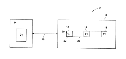
[0023] Referring now to the figures, there is illustrated in FIG. 1 an
exemplary
embodiment of a measurement system 10 with improved sensitivity and
construction, the
CA 02799731 2012-12-20
246080-11
latter of which is beneficial for implementation of the measurement system 10
at
operating temperatures greater than, e.g., 120 C, and in areas where access
by other
measurement systems is limited. The measurement system 10 can comprise a
transducer
array 12 and instrumentation 14, which is operatively coupled to the
transducer array 12
via a connection 16. The transducer array 12 can comprise one or more sensing
elements
18, each of the sensing elements 18 having a piezoelectric element 20 coupled
to a
substrate 22.
[0024] Transducer array 12 can be disposed on a target, such as a pipe, a
tube, and
related conduits that can be subject to corrosion and erosion by way of the
fluid that is
transported therein. The disposition of the transducer array 12 permits
ultrasonic signals
generated by the piezoelectric element 20 to impinge on the material of the
target. These
ultrasonic signals are reflected such as by surfaces of the material, wherein
the reflected
signals are detected by the piezoelectric element 20.
[0025] In one embodiment, instrumentation 14 can include an ultrasonic test
unit 24
that generates waveform pulses (generally, "inputs"), which are applied to the
piezoelectric element 20 via the connection 16. The waveform pulses cause a
mechanical
change (e.g., a dimensional change) in the piezoelectric element 20. This
change can
cause an acoustic wave, which is transmitted through the material of the
target.
Conversely, the piezoelectric element 20 generates a voltage difference when
acoustic
waves reflected from the material under inspection contact the surface of the
piezoelectric
element 20. This voltage difference is detected as receive signals (generally,
"outputs")
by the ultrasonic test unit 24 or other signal processing electronics.
[0026] The ultrasonic test unit 24 can include various control means, which
are useful
to determine the amplitude, timing, and transmit sequence of the waveform
pulse
generated by the piezoelectric element 20. The waveform pulse is generally in
the
frequency range of about 5 MHz to about 20 MHz. By tracking the difference
between
the transmission of the waveform pulse and the receipt of the received signal
and
measuring the amplitude of the reflected wave, various characteristics of the
material can
6
CA 02799731 2012-12-20
246080-11
be determined. In one example, the thickness of the material of the target, as
well as any
corresponding changes in the thickness, can be determined using time-of-flight
analysis,
the subject matter of which will be recognized by those artisans having skill
in the
transducer and related arts.
[0027] In one embodiment, the sensing elements 18 are separately arranged
and are
constructed as individual sensing units. Communication between these
individual units
and the ultrasonic test unit 24 is facilitated by the connection 16, and in
one construction
the connection 16 has a plurality of cables (not shown). These cables are
coupled to each
of the sensing elements 18. Exemplary cables can include coaxial cables and
optical
fibers, as well as single and plural strands of copper and/or related
materials that can
conduct the inputs and outputs (e.g., the waveform pulses and the received
signals) to and
from the piezoelectric element 20 as contemplated herein.
[0028] In another embodiment, the sensing elements 18 are arranged on a
common
substrate, generally demarcated in the present example with the numeral 26.
This
arrangement is defined by one or more of the piezoelectric elements 20 being
disposed on
the common substrate 26. The piezoelectric element 20 of the sensing elements
18 can
be spaced apart from one another along for example a strip of material, and as
discussed
in one or more embodiments below, this material can comprise a flexible
circuit material
that can conform to the shape of the target. In one example, conductors are
incorporated
in the flexible circuit material, with each conductor terminating at the
piezoelectric
element 20 and at the end of the common substrate 26. The connection 16 can
include
one or more connectors (not shown), which are coupled to the conductors, and
which can
be incorporated or otherwise affixed onto the free end. The connector can be
coupled to a
mating connector or other device such as a bundle of coaxial cables extending
from the
ultrasonic test unit 24. This combination can communicate the inputs and
outputs
between the piezoelectric element 20 and the instrumentation 14.
[0029] The number of the sensing elements 18 in the transducer array 12 can
vary,
and in one construction the number can vary from one to twenty. In one
particular
7
CA 02799731 2012-12-20
246080-11
example the number is fourteen. An alternative selection of the number can be
based on
any one or combination of the dimensions of the target under inspection, the
preferred
spacing of the sensing elements 18 on the target, and the type of defect being
detected.
When implemented in connection with the common substrate 26, the spacing
between the
approximate centers of the piezoelectric element 20 can be from about 10 mm to
about
100 mm. Moreover, in implementations where the sensing elements 18 are
arranged as
individualized units, each can be located on the target independently of other
ones of the
sensing elements 18 of the transducer array 12. Thus the space between
adjacent ones of
the piezoelectric element 20 and the location of the piezoelectric element 20
relative to
features (e.g., edges) of the target can be optimized for each of the sensing
elements 18 as
desired.
[0030] Although the transducer array 12 is depicted as a linear array
(e.g., wherein
the sensing elements 18 form a single row with one or more columns) other
configurations are also envisioned. In one embodiment, the transducer array 12
can
include one or more rows and one or more columns of sensing elements 18. In
another
embodiment, the sensing elements 18 are arranged in formations that are
different than
arrays of rows and columns. By way of example, one formation for transducer
array 12
can comprise a first row of sensing elements 18 and a second row of sensing
elements 18,
wherein the second row is positioned in perpendicular relation to the first
row, thus
forming a "t" shape.
[0031] Focusing now on the construction of the sensing elements 18,
reference can be
had to FIGS. 2 and 3. Here there is depicted an exemplary embodiment of a
piezoelectric
sensing device 100 which can be deployed as one or more of the sensing
elements 18 of
FIG. 1. In one embodiment, the piezoelectric sensing device 100 can comprise a
substrate 102 and a piezoelectric element 104 with a ceramic body 106. The
ceramic
body 106 can be configured with an electrode 108, a ground 110, and a wrap tab
112
constructed of gold plating or comparable conductive material that is
deposited on the
ceramic body 106. The substrate 102 can comprise a flexible circuit material
114, shown
8
CA 02799731 2012-12-20
246080-11
in this example with a first layer 116 and a second layer 118, and with a
receiving area
120 that is configured to receive the piezoelectric element 104. The receiving
area 120
can have electrodes 122 for connecting to, e.g., the electrode 108 and the
ground 110.
The electrodes 122 can include a first or ground electrode 124 and a second or
hot
electrode 126. The electrodes 122 can conform to an electrode geometry 128
that is
defined by an isolation gap 130 between the electrodes 122 and/or a shape
geometry 132
as applied to one or both of the electrodes 122. In one example the shape
geometry 132
comprises a t-shaped geometry 134 for the hot electrode 126.
[0032] In one embodiment, the piezoelectric sensing device 100 may also
include a
solder layer 136 that comprises one or more materials such as tin, lead,
silver, bismuth,
and indium. The solder layer 136 is deposited during assembly and is used to
couple the
piezoelectric element 104 to the receiving area 120 of the substrate 102. When
assembled, the combination of the substrate 102, the piezoelectric element
104, and the
solder layer 136 are arranged as a layered structure 138 with a profile height
P.
Embodiments of the piezoelectric sensing device 100 can be configured so that
the profile
height P does not exceed about 7 mm, and in one example the profile height is
from about
0.25 mm to about 1 mm. These values are smaller than conventional devices,
which
permits use of the piezoelectric sensing device 100 in places that are
generally not
accessible with measurement devices of conventional construction.
[0033] Materials for use in the ceramic body 106 are selected for their
properties
including for example compatibility with processing conditions during assembly
such as
the reflow temperatures required to reflow the solder layer 136. These reflow
temperatures typically are in excess of 200 C and in one exemplary process
the reflow
temperatures is about 220 C. Other properties to consider include, but are
not limited to,
dielectric constant of the material, wherein the materials that are selected
for the ceramic
body 106 should have a dielectric constant that renders good electrical
impedance
matching, while minimizing the overall dimensions of the piezoelectric element
104.
These dimensions include, for example, dimensions for the rectangular shape of
FIG. 2 of
9
246080-11
about 3 mm by about 5 mm, although the length and width can vary,
respectively, from
about 2 mm to about 8 mm. In other examples, the shape of the piezoelectric
element
104 can comprise a square, a circle, and/or an ellipse. With reference to the
profile height
P discussed above, it is further contemplated that piezoelectric element 104
is formed
with an overall thickness from about 0.1 mm to about 1 mm.
[0034] In one embodiment, it may be desirable to use piezoelectric
ceramics such as
Navy Type II materials and related ceramics (e.g., lead zirconium titanate
piezoelectric),
although other materials having similar properties and composition are
likewise
contemplated and may be used. For purposes of constructing the ceramic body
106 (and
the piezoelectric element 104 in general), in one example a brick of Navy Type
II
material can be diced into plates having a thickness on the order of 0.6 mm.
These plates
can be finished by way of finish grinding operations so that the thickness of
the resulting
plates is about 0.2 mm. Linear grinding, lapping, and back grinding are all
acceptable
finish grinding operations. The plates can thereafter be cut into strips with
a width of
about 9 mm and the electrodes can be formed, poled, and tested. Plating
operations such
as sputtering can be used to deposit the gold (Au) plating and the finished
plates can be
diced to form the individual piezoelectric elements (e.g., the piezoelectric
element 104).
In one example, a single brick of Navy Type II material can yield
approximately 2880 of
the piezoelectric element 104. It will be appreciated that the electrodes 122
can be
formed using certain deposition, etching, sputtering, and related processing
techniques
and processes recognized within the scope of the present disclosure.
[0035] The layers (e.g., the first layer 116 and the second layer 118) of
the flexible
circuit material 114 can comprise materials such as a polyamide-based film, as
well as
other materials and films that comprise one or more of polyester (PET),
polyimide (PI),
polyethylene napthalate (PEN), and polyetherimide (PEI). The layers can be
constructed
together to form a laminate that is compatible with the processing conditions,
operating
temperatures, and physical characteristics (e.g., the profile height P)
discussed herein.
Conductors such as electrical conductors like metal foil may be included among
the
CA 2799731 2017-10-20
CA 02799731 2012-12-20
246080-11
layers, or in other examples the conductors can be incorporated amongst the
layers such
as by using electroplating and related plating and deposition techniques.
These
conductors can extend to the electrodes 122 as well as to peripheral edges and
areas of
the substrate 102. This configuration is useful to conduct the pulse and
electrical signals
to and from the piezoelectric element 104, an example of which was discussed
above in
connection with the common substrate (e.g., the common substrate 26 of FIG.
1).
[0036] Referring next to FIGS. 4-9, there is provided exemplary embodiments
of a
piezoelectric sensing device 200 (FIGS. 4 and 5), 300 (FIGS. 6 and 7), and 600
(FIGS. 8
and 9). For purposes of the discussion that follows below, like numerals are
used to
identify like components as between FIGS. 2-9, except that the numerals are
increased by
a multiple of 100 (e.g.. 200 in FIGS. 4 and 5, 300 in FIGS. 6 and 7, 600 in
FIGS. 8 and
9). The piezoelectric sensing devices 200, 300, and 600 are useful for
implementation in
one or more of the configurations of the transducer array 12 discussed in
connection with
FIG. 1 above.
[0037] The piezoelectric sensing device 200 that is depicted in FIGS. 4 and
5, for
example, is suited for use in connection with the configuration of the
transducer array 12
(FIG. 1) wherein each of the sensing elements 18 is arranged as individual
units. In one
embodiment, the piezoelectric sensing device 200 can comprise a substrate 202
and a
piezoelectric element 204. The substrate 202 can comprise a flexible circuit
material 214
with a receiving area 220 in which is positioned the piezoelectric element
204. The
receiving area 220 can have electrodes 222 including a ground electrode 224
and a hot
electrode 226. A solder layer 236 can be disposed on one or more of the
electrodes 222
using screen printing techniques recognized in the art.
[00381 The flexible circuit material 214 can comprise a frontside 240 and a
backside
242 on which are located the electrodes 222. The piezoelectric sensing device
200 can
also comprise one or more cable connections 244 with cable connection pads 246
and
strain reliefs 248. The cable connection pads 246 can include a ground pad 250
and a hot
pad 252, each being coupled to, respectively, the ground electrode 224 and the
hot
11
CA 02799731 2012-12-20
246080-11
electrode 226 by way of one or more vias 254. The vias 254 extend through the
flexible
circuit material 214, thereby coupling the cable connection pads 246 on the
frontside 240
to the electrodes 222 on the backside 242. In one example, a ground plane 256
is also
incorporated into the flexible circuit material 214. The ground plane 256 is
coupled to
the ground electrode 224 and the ground pad 250.
[0039] The piezoelectric sensing device 300, as depicted in FIGS. 6 and 7,
can be
implemented when the transducer array 12 (FIG. 1) utilizes a common substrate
(e.g., the
common substrate 26 (FIG. 1)). In one embodiment, the piezoelectric sensing
device 300
can comprise a substrate 302 and a piezoelectric element 304. The substrate
302 can
comprise a flexible circuit material 314 with one or more receiving areas 320
configured
for receiving the piezoelectric element 304 thereon. The receiving areas 320
can have
electrodes 322 including a ground electrode 324 and a hot electrode 326. A
solder layer
336 is also included for securing the piezoelectric element 304 to the
electrodes 322.
[0040] The piezoelectric sensing device 300 can comprise a common substrate
358 in
which a plurality of conductors 360 are incorporated. The conductors 360 can
include
hot conductors 362 and ground conductors 364, each being illustrated as
extending from
a free end 366 of the common substrate 358. Disposed on the free end 366 is a
connector
368 such as a multi-pin connector that is coupled to each of the conductors
360. The
connector 368 is likewise configured to couple to a mating connector (not
shown) as
might be associated with the instrumentation (e.g., instrumentation 14 (FIG.
1))
contemplated herein.
[0041] The piezoelectric sensing device 600, as depicted in FIGS. 8 and 9,
can also
be implemented when the transducer array 12 (FIG. 1) utilizes a common
substrate (e.g.,
the common substrate 26 (FIG. 1)). The piezoelectric sensing device 600 can
have a first
side (or backside) 642 and a second side (or front side) 640. In one
embodiment, the
piezoelectric sensing device 600 can comprise a substrate 602 and a plurality
of
piezoelectric elements 604 mounted on the backside 642 of the substrate 602.
The
piezoelectric elements 604 can be ceramic piezoelectric transducers (PZT). The
substrate
12
CA 02799731 2012-12-20
246080-11
602 can comprise a flexible circuit 660 with a plurality of receiving areas
606 on the
backside 642 configured for mounting the piezoelectric elements 604 thereon.
[0042] The flexible circuit 660 can comprise a plurality of conductors 690.
The
conductors 690 can include hot conductors 632 and ground conductors 612, 622,
632
extending from a free or first end 696 of the flexible circuit 660. Disposed
on the free
end 696 can be a connector 698 such as a multi-pin connector that is coupled
to each of
the conductors 690. The connector 698 is likewise configured to couple to a
mating
connector (not shown) as might be associated with the instrumentation (e.g.,
instrumentation 14 (FIG. 1)) contemplated herein.
[0043] The flexible circuit 660 of the piezoelectric sensing device 600 can
comprise a
plurality of different layers. In one embodiment illustrated in FIG. 9, the
flexible circuit
660 has a double-sided copper-cladded core 610, including a pure polyimide C-
stage core
620 between a first copper layer on the back side 642 and a second copper
layer on the
front side 640. As a C-stage material, the core 620 is fully cured and is
therefore
relatively insoluble and infusible. In one embodiment, the core 620 can be
0.005 in.
(0.127 mm) thick. The copper layers of the double-sided copper-cladded core
610 can be
etched with, e.g., chemicals, to form a plurality of conductors 612, 622, 632
on the front
side 640 and the backside 642 of the pure polyimide C-stage core 620. In one
embodiment, the copper layers 640, 642 can be 0.0007 in. (0.0178 mm) thick. As
shown
in FIG. 9, the etching can provide an isolation gap 650 between the backside
ground
conductors 612 and the backside hot conductors 632. A plurality of plated vias
630
extending through the pure polyimide C-stage core 620 can be used to connect
the
backside ground conductors 612 and the front side ground conductors 622.
[0044] In one embodiment of the piezoelectric sensing device 600
illustrated in FIG.
9, the flexible circuit 660 has glass reinforced polyimide C-stage cover
layers 616. 626
formed over the conductors 612, 622, 632. In one embodiment, the glass
reinforcement
can be woven fibreglass with a 1080 glass type. Before processing (e.g.,
laminating), as a
B-stage prepreg material (e.g., low flow polyimide 1080 prepreg), the backside
cover
13
CA 02799731 2012-12-20
246080-11
layer 616 and the front side cover layer 626 are partially cured and such that
they are not
completely fused or dissolved, but rather soften when heated and swell in
contact with
certain liquids. After processing, the cover layers 616, 626 are fully cured
to a C-stage
material. Windows 608 can be formed in the backside cover layer 616 to form
the
receiving areas 606 configured for receiving the piezoelectric elements 604
thereon and
to expose a ground electrode 618 and a hot electrode 638 in each window. A
first solder
layer 603 secures the piezoelectric element 604 to the ground electrode 618
and a second
solder layer 605 secures the piezoelectric element 604 to the hot electrode
638. Given the
material properties of the glass reinforced polyimide C-stage cover layers
616, 626, a
laser or other cutting technique may be used to form the windows 608 if
etching cannot
be used to remove the glass reinforced polyimide C-stage material.
[0045] To facilitate soldering, the conductors 612, 622, 632 can be plated
with plating
layers 614, 624. In one embodiment, the plating can be 0.0005 in. (0.0127 mm)
thick. In
one embodiment, electrolysis nickel over immersion gold (ENIG) is used to
plate the
conductors 612, 622, 632 before the cover layers 616, 626 are formed over the
conductors
612, 622, 632. In another embodiment, ENIG is used to plate the conductors
612, 622,
632 with the plating layers only after the cover layers 616, 626 are formed
over the
conductors 612, 622, 632 and the windows 606 are formed to expose the
conductors 612,
622, 632 for plating.
[0046] The pure polyimide C-stage core 620 and the glass reinforced
polyimide C-
stage cover layers 616, 626 provide the flexibility and support necessary for
the flexible
circuit 660 to be installed on curved surfaces of a conduit or other
circumferential
devices. The use of a pure polyimide C-stage core 620 and glass reinforced
polyimide C-
stage cover layers 616, 626 also eliminates impurities or other additives that
may
decrease the temperature rating of the piezoelectric sensing device 600 and
allow the
piezoelectric sensing device 600 to operate in environments and on devices
that are
routinely operating well above 120 C (e.g., nuclear power generation
environments).
14
CA 02799731 2012-12-20
246080-11
[00471 In one
embodiment, the glass reinforced polyimide C-stage cover layers 616,
626 can be formed over the conductors 612, 622, 632 by providing glass-
reinforced
polyimide B-stage sheets on the front side 640 and the backside 642 of the
pure
polyimide C-stage core 620, which can also be provided in a sheet, and
compressing the
polyimide layers between two presses while exposing the layers to temperatures
that will
form the flexible circuit 660 after lamination. The use of the described
polyimide layers
can avoid the need for using epoxies or other adhesive materials that may have
lower
temperature ratings than the glass reinforced polyimide cover layers 616, 626
and the
pure polyimide C-stage core 620.
[0048] Discussing
now the implementation of piezoelectric sensing devices such as
the piezoelectric sensing devices 100, 200, 300, and 600 discussed above,
reference is
now directed to FIGS. 10 and 11. FIGS. 10 and 11 illustrate, respectively
exemplary
embodiments of a piezoelectric sensing device 400 and 500, these embodiments
being
configured for use in measurement systems such as the measurement systems
described
above and in more detail below. Like numerals are also used to identify like
components
as between the FIGS. 2-11. However, although some of the features and concepts
of the
piezoelectric sensing devices of the present disclosure may not be depicted or
discussed
in connection with FIGS. 10 and 11, it is contemplated that such features and
concepts
are applicable to the piezoelectric sensing devices 400 and 500 as well as
embodiments
and derivation thereof
[0049] There is
depicted in FIG. 10, for example, a plurality of piezoelectric sensing
devices 400, each of which can comprise a substrate 402 and a piezoelectric
element 404.
The substrate 402 can include a flexible circuit material 414 with a ground
electrode 424,
a hot electrode 426, and a solder layer 436 that is used to secure the
piezoelectric element
404 to the substrate 402. The flexible circuit material 414 includes a
frontside 440 and a
backside 442. In one
embodiment, the piezoelectric sensing devices 400 are
implemented as part of a measurement system 470, which can comprise a
transducer
array 472, instrumentation 474, and a connection 476 such as one or more
cables 478 that
CA 02799731 2012-12-20
246080-11
are coupled to the piezoelectric element 404. The measurement system 470 can
also
comprise a connection terminal 480 to aggregate the cables 478, acting in one
example as
a central hub for communicating signals to and from the instrumentation 474
and the
piezoelectric sensing devices 400 of the transducer array 472.
[0050] In one embodiment, the piezoelectric sensing devices 400 are secured
to a
surface 482 of a target 484 using a couplant 486 such as an adhesive that is
disposed on
the backside 442 of the substrate 402. To further ensure proper functioning
and coupling
of the piezoelectric sensing devices 400 to the surface 482, one or more outer
structures
488 can be utilized such as a protective layer 490 and a fastening mechanism
492. These
outer structures 488 can be incorporated as part of the piezoelectric sensing
devices 400
or in one embodiment the outer structures 488 comprise one or more pieces
separate from
the piezoelectric sensing devices 400. Assembly of the pieces of the outer
structures 488
can occur at the time of implementation and installation of piezoelectric
sensing devices
400 and the measurement system 470 generally.
[0051] The couplant 486 can be disposed on surfaces of the substrate 402,
as depicted
in FIG. 10, as well as on the piezoelectric element 404. Care should be taken
during
application to avoid degradation of the performance of the piezoelectric
element 404. In
addition to performance characteristics, it may be desirable that materials
for use as the
couplant 486 are compatible with the material characteristics of the substrate
402 and the
target 484. In one example, adhesives such as acrylic adhesives can be applied
at as a
layer with a nominal initial thickness of about 1 mm. Other adhesives and
related
materials that may be likewise acceptable include, but are not limited to,
cyanocrylates,
epoxies, solvent-based adhesives, and cold-flow adhesives, as well as
combinations and
derivations thereof
[0052] The protective layer 490 is used to prevent damage to the underlying
structure,
e.g., the piezoelectric sensing devices 400. Materials can likewise have
electrically
insulating properties thus providing protection from the outer environment as
well as
preventing arcing, shorting, and other electrical-induced failures that can
occur.
16
246080-11
Exemplary materials for use as the protective layer 490 can include silicon,
nylon,
neoprene, polymeric materials, and combinations and derivations thereof.
[0053] The
fastening mechanism 492 can be in the form of the band-like structure
illustrated in FIG. 11. When the target 484 is a conduit or other
circumferential device,
such structures can be affixed about the circumference. These structures can
incorporate
secondary fastening and tightening features that reduce the diameter of the
band about the
conduit, thereby applying a force onto the piezoelectric sensing devices 400.
For other
configurations of the target 484, such as for targets with flat or irregular
constructions,
the fastening mechanism 492 may be configured with devices that are designed
for the
specific configuration of the target 484. These devices may include magnets
and
magnetized implements that can cause to be applied to force onto the
piezoelectric
sensing devices 400.
[0054] Referring
now to FIG. 11, it is seen that the piezoelectric sensing device 500
can comprise a substrate 502 and a piezoelectric element 504. The substrate
502 can
comprise a ground electrode 524 and a hot electrode 526, and a solder layer
536 is
included as contemplated herein. The substrate 502 is arranged as a common
substrate
558 with a free end 566 on which is disposed a connector 568. The
piezoelectric sensing
device 500 is part of a measurement system 570, which can comprise a
transducer array
572, instrumentation 574, and a connection 576 coupled therebetween. To secure
the
piezoelectric sensing device 500, a couplant 586 is used and further
protection is afforded
by a protective layer 590 and a fastening mechanism 592. In one embodiment,
the
connection 576 can comprise a single cable 594 that is coupled to the
connector 568 and
to the instrumentation 574. The single cable 594 can comprise, for example, a
mating
connector 596 that is configured to mate with the connector 568.
[0055] This written
description uses examples to disclose embodiments of the
invention, including the best mode, and also to enable any person skilled in
the art to
practice the invention, including making and using any devices or systems and
performing any incorporated methods. The patentable scope of the invention may
include
17
CA 2799731 2017-10-20
246080-11
other examples that occur to those skilled in the art in view of the
description. Such other
examples are intended to be within the scope of the invention.
18
CA 2799731 2017-10-20