Note: Descriptions are shown in the official language in which they were submitted.
CA 02800847 2014-10-28
UNCOOLED INFRARED DETECTOR AND
METHODS FOR MANUFACTURING THE SAME
BACKGROUND
[0002] 1. Field
[0003] The present invention generally relates to the field of infrared
detectors, and more
particularly to uncooled infrared detectors that are manufactured from foundry-
defined
silicon-on-insulator (SOI) complementary metal oxide semiconductor (CMOS)
wafers.
[0004] 2. Description of the Related Art
[0005] An uncooled (thermal) infrared detector is a device including a
pixel with an
infrared absorption layer (a.k.a. heat absorption layer) and a thermoelectric
conversion
element. The infrared absorption layer receives and converts an infrared ray
(wave) into heat.
The thermoelectric conversion element converts the heat into an electric
signal that
communicates the characteristics of the received infrared ray.
[0006] Conventional uncooled infrared detectors may have an array of
pixels, each of
which may include a single diode for performing the function of the
thermoelectric
conversion element. Generally, the single diode may have a turn-on voltage
that depends on
the temperature of the heat absorption layer. When the single diode conducts a
constant
current, the potential difference across the single diode may vary with the
heat converted by
the heat absorption layer. As such, the potential difference of the single
diode may be used
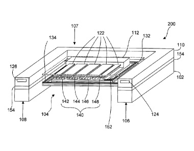
for measuring the intensity of the received infrared ray.
1
CA 02800847 2012-10-11
WO 2011/130284
PCT/US2011/032136
[0007] In order
to prevent the heat from transferring among pixels, conventional
uncooled infrared detectors use various types of closed well structures to
thermally isolate
each pixel. Typically, a closed well may be formed on the substrate layer, and
it may define
a cavity that surrounds the pixel. A support structure may be formed between
the closed well
and the pixel for suspending the pixel within the cavity. The suspended pixel,
the closed
well, and the support structures may be fabricated on a silicon substrate by
using customer-
specific fabrication processes.
[0008] However,
these customer-specific fabrication processes generally involve several
iterations of high precision lithography, each of which may be costly and time
consuming to
perform. Moreover, these customer-specific fabrication processes may suffer
from low yield
because the failure rates of high precision lithography are statistically
high. In exchange for a
better yield, some conventional infrared detectors may sacrifice the
reliability of the pixels,
the closed wells, and/or the support structures.
[0009] Thus,
there is a need for an uncooled infrared detector with improved quality,
higher yield, and lower production cost.
SUMMARY
[0010] The
present invention may provide several solutions to satisfy the need as
identified in the previous section. One of the solutions may include various
methods for
manufacturing the uncooled infrared detectors by using foundry-defined silicon-
on-insulator
(SOI) complementary metal oxide semiconductor (CMOS) wafers. Generally, a
foundry-
defined SOI-CMOS wafer may be fabricated by using a generic SOI-CMOS process
(a.k.a.
standard SOI-CMOS process).
[0011] The
generic SOI-CMOS process may be defined and offered by one or more
foundries (e.g., fabrication companies that fabricate SOI-CMOS wafers). The
generic SOI-
CMOS process may fulfill the design requirements of many customers. As such,
the generic
2
CA 02800847 2012-10-11
WO 2011/130284
PCT/US2011/032136
SOI-CMOS process typically involves standard design rules, process sequence,
and/or
process parameters, which may reduce the time and cost for fabricating the
foundry-defined
SOI-CMOS wafers. Moreover, because of its standardization nature, the SOI-CMOS
wafers
fabricated according to the generic SOI-CMOS process can be adopted by other
applications.
Due to the economies of scale, the production cost of foundry-defined SOI-CMOS
wafers
(a.k.a. standard SOI-CMOS wafers) can be substantially reduced.
[0012] The manufacturing methods disclosed herein involve a few process
steps for
modifying the foundry-defined SOI-CMOS wafers. The modification may allow the
SOI-
CMOS wafers to incorporate the functional and structural features of the
uncooled infrared
detectors. When compared to conventional lithography and deposition steps,
these process
steps may be cost efficient and easy to perform because they have a relatively
high tolerance
margin (a.k.a. non-critical). Advantageously, the methods disclosed herein may
allow the
cost and yield of the uncooled infrared detectors to be improved tremendously.
[00131 In one embodiment, the present invention may be a silicon-on-
insulator (SOI)
complementary metal oxide semiconductor (CMOS) wafer for use in manufacturing
an
uncooled microbolometer. The SOI-CMOS wafer may include a substrate layer, an
insulation layer formed on the substrate layer, the insulation layer having a
pixel region and a
wall region surrounding the pixel region, a pixel structure formed on the
pixel region of the
insulation layer, a wall structure formed adjacent to the pixel structure and
on the wall region
of the insulation layer, a dielectric layer covering the pixel structure and
the wall structure, a
pixel mask formed within the dielectric layer, and for protecting the pixel
structure during a
dry etching process, and a wall mask formed within the dielectric layer, and
for protecting the
wall structure during the dry etching process, thereby releasing a space
defined between the
wall structure and the pixel structure after the dry etching process.
3
CA 02800847 2012-10-11
WO 2011/130284
PCT/US2011/032136
[0014] In another
embodiment, the present invention may provide an infrared detector
manufactured from a foundry-defined silicon-on-insulator (SOI) complementary
metal oxide
semiconductor (CMOS) wafer. The infrared detector may include a plurality of
walls
forming a through well defining a first opening and a second opening opposing
the first
opening, an infrared sensor configured to detect an infrared wave passing
through one of the
first opening or the second opening of the through well, and a support arm
connecting the
sensor to at least one of the plurality of walls so as to suspend the infrared
sensor within the
through well and adjacent to the first opening.
[0015] In another
embodiment, the present invention may provide a method for
manufacturing an uncooled infrared detector from a foundry-defined silicon-on-
insulator
(SOI) complementary metal oxide semiconductor (CMOS) wafer having a substrate
layer, an
insulation layer formed on the substrate layer and having a pixel region and a
wall region
surrounding the pixel region, a pixel structure formed on the pixel region of
the insulation
layer, a wall structure formed adjacent to the pixel structure and on the wall
region of the
insulation layer, a dielectric layer covering the pixel structure and the wall
structure, a pixel
mask formed within the dielectric layer and covering the pixel structure, and
a wall mask
formed within the dielectric layer and covering the wall structure. The method
may include
the steps of performing a first vertical etching through a portion of the
substrate layer to
define a back pixel space terminated by the pixel region of the insulation
layer, performing a
second vertical etching through a portion of the dielectric layer not covered
by the pixel mask
and the wall mask and through a portion of the insulation layer not covered by
the pixel mask
and the wall mask, so as to define a front pixel space for separating the
pixel structure from
the wall structure, and removing the pixel mask and the wall mask.
[0016] In yet
another embodiment, the present invention may provide a method for
manufacturing an uncooled infrared detector from a foundry-defined silicon-on-
insulator
4
CA 02800847 2012-10-11
WO 2011/130284
PCT/US2011/032136
(SOI) complementary metal oxide semiconductor (CMOS) wafer having a substrate
layer, an
insulation layer formed on the substrate layer and having a pixel region and a
wall region
surrounding the pixel region, a pixel structure formed on the pixel region of
the insulation
- layer, a wall structure formed adjacent to the pixel structure and on the
wall region of the
insulation layer, a dielectric layer covering the pixel structure and the wall
structure, a pixel
mask formed within the dielectric layer and covering the pixel structure, and
a wall mask
formed within the dielectric layer and covering the wall structure. The method
may include
the steps of performing a vertical etching through a portion of the dielectric
layer not covered
by the pixel mask and the wall mask and through a portion of the insulation
layer not covered
by the pixel mask and the wall mask, so as to define a front pixel space for
separating the
pixel structure from the wall structure, removing the pixel mask and the wall
mask, and
performing an anisotropic silicon etching to form a well on the substrate
layer and under the
pixel structure, the well defining a back pixel space joining the front pixel
space for thermally
isolating the pixel structure from the substrate layer and the wall structure.
[0017] This summary is provided merely to introduce certain concepts and
not to identify
any key or essential features of the claimed subject matter.
BRIEF DESCRIPTION OF THE DRAWINGS
[0018] Other systems, methods, features, and advantages of the present
invention will be
or will become apparent to one with skill in the art upon examination of the
following figures
and detailed description. It is intended that all such additional systems,
methods, features,
and advantages be included within this description, be within the scope of the
present
invention, and be protected by the accompanying claims. Component parts shown
in the
drawings are not necessarily to scale, and may be exaggerated to better
illustrate the
important features of the present invention. In the drawings, like reference
numerals
designate like parts throughout the different views, wherein:
CA 02800847 2012-10-11
WO 2011/130284
PCT/US2011/032136
[0019] FIG. 1
shows a top view of an infrared detector pixel according to an embodiment
of the present invention;
[0020] FIG. 2A
shows a perspective view of an infrared detector pixel according to an
embodiment of the present invention;
[0021] FIG. 2B
shows a cross-sectional view of the infrared detector pixel according to
an embodiment of the present invention;
[0022] FIGS. 3A ¨
3H show the cross-sectional views of a foundry-defined silicon-on-
insulator (SOI) complementary metal oxide semiconductor (CMOS) wafer being
processed to
form a through well microbolometer according to an embodiment of the present
invention;
[0023] FIGS. 4A ¨
4F show the cross-sectional views of the foundry-defined SOI-CMOS
wafer being processed to form a closed well microbolometer according to an
embodiment of
the present invention;
[0024] FIG. 5A
shows a perspective view of an infrared detector pixel with a heat
absorption umbrella according to an embodiment of the present invention;
[0025] FIG. 5B
shows a cross-sectional view of the infrared detector pixel with a heat
absorption umbrella according to an embodiment of the present invention;
[0026] FIGS. 6A ¨
6F show the cross-sectional views of a foundry-defined silicon-on-
=
SOI-CMOS wafer being processed to form a through well microbolometer with heat
absorption umbrellas according to an embodiment of the present invention; and
[0027] FIGS. 7A ¨
7B show the cross-sectional views of a post-CMOS processed wafer
being further processed to form a closed well microbolometer with a heat
absorption
umbrella according to an embodiment of the present invention.
DETAILED DESCRIPTION
[0028] Apparatus,
systems and methods that implement the embodiment of the various
features of the present invention will now be described with reference to the
drawings. The
6
CA 02800847 2012-10-11
WO 2011/130284
PCT/US2011/032136
drawings and the associated descriptions are provided to illustrate some
embodiments of the
present invention and not to limit the scope of the present invention.
Throughout the
drawings, reference numbers are re-used to indicate correspondence between
reference
elements. In addition, the first digit of each reference number indicates the
figure in which
the element first appears.
[0029] FIG. 1 shows a top view of an infrared detector pixel 100 according
to an
embodiment of the present invention. The infrared detector pixel 100 may be a
single
sensing unit, such that it may be duplicated and arranged to form a
microbolometer focal
plane array (FPA). The infrared detector pixel 100 may include a pixel wall
101, a pixel
island 104, a first (right) support arm 132, and a second (left) support arm
134.
[0030] The pixel wall 101 may have a rectangular (e.g., a square) cross-
sectional frame,
which defines a thermal isolation space 103. The pixel island 104 may be
positioned within
the thermal isolation space 103 but without contacting the pixel wall 101. The
first support
arm 132 and the second support arm 134 may mechanically connect the pixel
island 104 to
the interior of the pixel wall 101. As such, the first support arm 132 and the
second support
arm 134 may suspend the pixel island 104 within the thermal isolation space
103.
[0031] The thermal isolation space 103 may provide thermal isolation
between the pixel
island 104 and the pixel wall 101, which may be shared by an adjacent infrared
detect pixel
(not shown). Accordingly, the thermal isolation space 103 may help prevent or
slow down
the transfer of heat between the pixel island 104 and the pixel wall 101. In
one embodiment,
the pixel wall 101 may form a through well with a first opening and a second
opening. As
such, the thermal isolation space 103 may be a through space that extends
through the first
opening and the second opening. In another embodiment, the pixel wall 101 may
form a
closed well with only one opening. As such, the thermal isolation space 103
may be a semi-
through space that extends though only one opening of the closed well.
7
CA 02800847 2012-10-11
WO 2011/130284
PCT/US2011/032136
[0032] The pixel island 104 may include a heat absorption layer 112 and a
diode group
140. The heat absorption layer 112 may receive the infrared ray (wave) and
retain heat
energy extracted from the infrared ray. In one embodiment, the heat absorption
layer 112
may completely encapsulate the diode group 140. In another embodiment, the
heat
absorption layer 112 may substantially cover the diode group 140. In any
event, the heat
absorption layer 112 may have an internal temperature that indicates the
characteristics of the
received infrared ray. To enhance the infrared ray retention characteristics
of the heat
absorption layer 112, a layer of titanium, titanium nitride, and/or other
similar material may
be deposited on or formed within the heat absorption layer 112.
[0033] The diode group 140 may include one or more diodes, each of which
may have a
turn-on voltage that is controlled by the internal temperature of the heat
absorption layer 112.
In one embodiment, each diode may have a turn-on voltage that is different
than the other
diodes. In another embodiment, all the diodes may share similar turn-on
voltages. By
varying the turn-on voltages of the diodes, the infrared detector pixel 100
may provide an
enhanced sensitivity to the incident infrared ray. The diodes may be arranged
in various
configurations. In one embodiment, for example, the diodes of the diode group
140 may be
connected serially to form a diode chain. In another embodiment, for example,
the diodes of
the diode group 140 may be connected in parallel to form a diode net.
[0034] FIG. 2A shows a perspective view of an infrared detector pixel 200
according to
an embodiment of the present invention. The infrared detector pixel 200 may
share several
interchangeable features with the infrared detector pixel 100. Additionally,
the infrared
detector pixel 200 may include functional and structural features that are
different from those
of the infrared detector pixel 100. The detector pixel 200 may include four
pixel walls.
However, for purpose of illustrating the internal structure of the infrared
detector pixel 200,
only the first (right) pixel wall 106, the second (back) pixel wall 107, and
the third (left) pixel
8
CA 02800847 2012-10-11
WO 2011/130284
PCT/US2011/032136
wall 108 are shown, while the fourth (front) pixel wall is omitted. The four
pixel walls may
join one another to form a through pixel well, which may define a first (top)
opening, a
second (bottom) opening, and a through space positioned between the first
opening and the
second opening.
[0035] Each of the pixel walls (e.g., the first, second, and third pixel
walls 106, 107, and
108) may include a pixel wall oxide layer 110, a pixel wall insulating (buried
oxide) layer
154, and a pixel wall substrate layer 102. Optionally, each of the pixel walls
(e.g., the first,
second, and third pixel walls 106, 107, and 108) may include one or more
electrical wire for
conducting electrical signal between a readout circuit (not shown) and the
diode group 140.
[0036] In one embodiment, for example, the first pixel wall 106 may
encapsulate a first
readout wire 124 within the pixel wall oxide layer 110. In another embodiment,
for example,
the third pixel wall 108 may encapsulate a second readout wire 126 within the
pixel wall
oxide layer 110. The first readout wire 124 and the second readout wire 126
may each be
used for carrying a digital signal, an analog signal, a biasing signal, an
input signal, a column
select signal, a row selection signal, and/or other signals for controlling
the operation of the
diode group 140. The first readout wire 124 and the second readout wire 126
may be part of
a Metal-1 layer, a Metal-2 layer and/or a Metal-3 layer, each of which may
include a
conducting metal, such as copper, gold, and/or aluminum.
[0037] The infrared detector pixel 200 may include the pixel island 104,
which may be
suspended above the substrate layer 102 of the through pixel well, such that
the pixel island
104 may be thermally isolated from the pixel walls (e.g., the first, second,
and third pixel
walls 106, 107, and 108). The pixel island 104 may include an island
insulation (buried
oxide) layer 152, the heat absorption layer 112, and the diode group 140. The
island
insulation layer 152 may be horizontally aligned with the pixel wall
insulation layer 154. The
9
CA 02800847 2012-10-11
WO 2011/130284
PCT/US2011/032136
heat absorption layer 112 may be horizontally aligned with the pixel wall
oxide layer 110,
and it may include multiple dielectric layers and anti-reflection layers.
[0038] In one embodiment, the heat absorption layer 112 may be made of the
same
material as the pixel wall oxide layer 110. In another embodiment, the heat
absorption layer
112:may be made of a material that is different from that of the pixel wall
oxide layer 110. In
another embodiment, the heat absorption layer 112 may include a dielectric
material, such as
a nitride material and/or an oxide material. In yet another embodiment, the
heat absorption
layer 112 may include an anti-reflective material, such as a titanium
material, a titanium
nitride material, and/or other material with similar physical and chemical
properties.
Together, the heat absorption layer 112 and the island insulation layer 152
may substantially
encapsulate the diode group 140.
[0039] The infrared detector pixel 100 may be deployed in a flip-chip
configuration, in
which the island insulation layer 152 may be oriented as the top side of the
infrared detector
pixel 100. Accordingly, the island insulation layer 152 may be used as a heat
absorption
layer. A titanium layer, a titanium nitride layer, and/or a layer with other
material with
similar physical and chemical properties may be deposited on the insulation
layer 152 to
enhance the infrared ray retention characteristic thereof.
[0040] The diode group 140 may include a plurality of diodes, such as a
first diode 142, a
second diode 144, a third diode 146, and a fourth diode 148. Each of the
diodes (e.g., the
first, second, third, and fourth diodes 142, 144, 146, and 148) may have a
turn-on voltage that
is adjustable by the internal temperature of the heat absorption layer 112.
However, the turn-
on voltage of each of the diodes (e.g., the first, second, third, and fourth
diodes 142, 144, 146,
and 148) may or may not be the same as one another. In one embodiment, for
example, the
diodes may share the same turn-on voltage. In another embodiment, for example,
the diodes
CA 02800847 2012-10-11
WO 2011/130284
PCT/US2011/032136
may have various progressive turn-on voltages. In yet another embodiment, for
example, the
diodes may have various linear turn-on voltages.
[0041] The first diode 142, the second diode 144, the third diode 146, and
the fourth
diode 148 may each have a p-n junction that is perpendicular to the island
insulation layer
152 and to the substrate layer 102 of the pixel wall. The first diode 142, the
second diode
144, the third diode 146, and the fourth diode 148 may be connected serially
to form a diode
chain. In one embodiment, the pixel island 104 may include a plurality of
inter-diode
metallic plates 122, each of which may connect the opposite junctions of a
pair of diodes.
[0042] In addition to providing electrical connection among the diode group
140, the
inter-diode metallic plates 122 may function as a series of internal
reflecting surface for the
heat absorption layer 112. Because the turn-on voltages of the diodes (e.g.,
the first diode
142, the second diode 144, the third diode 146, and/or the fourth diode 148)
are controlled by
temperature, but not directly by the received infrared ray, it may be
desirable to use the inter-
diode metallic plates 122 to reflect the unabsorbed infrared ray back to the
heat absorption
layer 112 for further absorption. In return, the heat absorption layer 112 may
further convert
the reflected infrared ray to heat. In one embodiment, the inter-diode
metallic plates 122 may
be extended to cover the entire horizontal cross sectional surface of the heat
absorption layer
112 in order to maximum the reflection functionality thereof.
[0043] The electrical signal carried by the inter-diode metallic plates 122
may be
communicated to a readout circuit via the first support arm 132 and/or the
second support
arm 134. In one embodiment, for example, the first support arm 132 may provide
electrical
and/or mechanical connections between the pixel island 104 and the third pixel
wall 108. In
another embodiment, for example, the second support arm 134 may provide
electrical and/or
mechanical connections between the pixel island 104 and the first pixel wall
106.
11
CA 02800847 2012-10-11
WO 2011/130284
PCT/US2011/032136
[0044] As shown in FIG. 2B, each of the first support arm 132 and the
second support
arm 134 may include similar layers as the pixel walls (e.g., the first,
second, and/or third
pixel walls 106, 107, and/or 108) and the pixel island 104. In one instance,
the first support
arm 132 and the second support arm 134 may each include a support arm
insulation layer
156, which may be horizontally aligned with the island insulation layer 152
and the pixel wall
insulation layer 154. In another instance, the first support arm 132 and the
second support
arm 134 may each include a support arm oxide layer 114, which may be
horizontally aligned
with the pixel wall oxide layer 110 and the heat absorption layer 112. The
support arm oxide
layer 114 may provide mechanical support for the pixel island 104, and it may
prevent the
transfer of heat between the pixel island 104 and the pixel walls (e.g., the
first pixel wall 106
and/or the third pixel wall 108).
[0045] The first support arm 132 may include a first polysilicon wire 135,
which may be
encapsulated by the support arm oxide layer 114. The first polysilicon wire
135 may
establish an electrical coupling between the inter-diode metallic plates 122
and the first
readout wire 124 of the first pixel wall 106. The second support arm 134 may
include a
second polysilicon wire 137, which may be encapsulated by the support arm
oxide layer 114.
The second polysilicon wire 137 may establish an electrical coupling between
the inter-diode
metallic plates 122 and the second readout wire 126 of the first pixel wall
106. While other
conducting material may be used for forming the conducting wires in the first
support arm
132 and/or the second support arm 134, polysilicon may be preferred because of
its relatively
low thermal conductance.
[0046] In addition to the first readout wire 124, the first pixel wall 106
may include a
third readout wire 164. Generally, the third readout wire 164 may conduct
similar signals as
the first readout wire 124. The third readout wire 164 may be a part of a
higher metal layer
than the first readout wire 124. As such, the third readout wire 164 may be
used for global
12
CA 02800847 2012-10-11
WO 2011/130284
PCT/US2011/032136
routing while the first readout wire 124 may be used for local and/or inter-
pixel routings.
Similarly, in addition to the second readout wire 126, the third pixel wall
108 may include a
fourth readout wire 166. Generally, the fourth readout wire 166 may conduct
similar signals
as the second readout wire 126. The fourth readout wire 166 may be a part of a
higher metal
layer than the second readout wire 126. As such, the fourth readout wire 166
may be used for
global routing while the second readout wire 126 may be used for local and/or
inter-pixel
routings.
[0047] The discussion now turns to various methods for manufacturing
uncooled infrared
detectors (e.g., the infrared detector pixels 100 and 200) by using foundry-
defined silicon-on-
insulator (SOI) complementary metal oxide semiconductor (CMOS) wafers. A SOI-
CMOS
wafer may be fabricated by using a SOI-CMOS process. Generally, the SOI-CMOS
process
may be customer-specific or generic.
[0048] The customer-specific SOI-CMOS process may be defined by individual
customers based on their particular design goals. The customer-specific SOI-
CMOS process
of one customer may or may not fulfill the design goals of another customer.
As such, the
customer-specific SOI-CMOS process typically involves specific design rules,
process
sequence, and/or process parameters. These specific requirements may increase
the time and
cost for fabricating the SOI-CMOS wafers. Moreover, because of its specific
nature, the
SOI-CMOS wafers fabricated according to the customer-specific SOI-CMOS process
are
unlikely to be adopted by other applications. Therefore, the production cost
of customer-
specific SOI-CMOS wafers is generally high.
[0049] On the other hand, the generic SOI-CMOS process (a.k.a. standard SOI-
CMOS
process) may be defined and offered by one or more foundries (e.g.,
fabrication companies
that fabricate SOI-CMOS wafers). The generic SOI-CMOS process may fulfill the
design
requirements of the many customers. As such, the generic SOI-CMOS process
typically
13
CA 02800847 2012-10-11
WO 2011/130284
PCT/US2011/032136
involves standard design rules, process sequence, and/or process parameters,
which may
reduce the time and cost for fabricating the foundry-defined SOI-CMOS wafers.
Moreover,
because of its generic nature, the SOI-CMOS wafers fabricated according to the
generic SOI-
CMOS process are likely to be adopted by other applications. Due to the
economies of scale,
the production cost of foundry-defined SOI-CMOS wafers (a.k.a. standard SOI-
CMOS
wafers) is much lower than that of the customer-specific SOI-CMOS wafers.
[0050] The methods disclosed herein may involve a few process steps for
modifying the
foundry-defined SOI-CMOS wafers. The modification may allow the SOI-CMOS
wafers to
incorporate the functional and structural features of the uncooled infrared
detector (e.g., the
uncooled infrared detector pixels 100 and 200). These process steps may be
cost efficient
and easy to perform because they have a relatively high tolerance margin
(a.k.a. non-critical)
when compared to conventional lithography and deposition steps.
Advantageously, the
methods disclosed herein may allow the cost and yield of the uncooled infrared
detectors to
be improved tremendously.
[0051] Generally, a foundry-defined SOI-CMOS wafer may include a substrate
layer, an
insulation layer, and a dielectric layer. The substrate layer may provide
structural support for
the insulation layer and the dielectric layer. The insulation layer may be
formed on the
substrate layer, and it may define at least one pixel region and at least one
wall region. The
wall region may, partially or completely, surround the pixel region, but
without contacting
the pixel region. As such, a space may be defined between the pixel region and
the wall
region.
[0052] Depending on the design goal, the pixel region and the wall region
may have
various shapes. In one embodiment, for example, the pixel region may have a
square shape
and the wall region may have a square frame shape. In another embodiment, for
example, the
pixel region may have a circular shape and the wall region may have a
circumferential shape.
14
CA 02800847 2012-10-11
WO 2011/130284
PCT/US2011/032136
In yet another embodiment, for example, the pixel region may have a hexagonal
shape and
the wall region may have a hexagonal frame shape.
[0053] The dielectric layer may be formed on top of the insulation layer,
and it may
cover, and be used for composing, one or more pixel structures, wall
structures, biasing
circuits, and/or readout circuits. The pixel structure may include a diode
group (e.g., the
diode group 140). The diode group may include similar functional and
structural features as
the diode group 140 as previously discussed. The diode group may include one
or more
doped silicon material, and it may be formed on the insulation layer (hence
the term "SOI").
[0054] The dielectric layer may include multiple layers, each of which may
include an
oxide material, a nitride material, and/or other dielectric materials. The
dielectric layer may
be embedded with multiple mask layers, each of which may be designated to
protect a
particular structure (e.g., the pixel structure, the wall structure, the
biasing circuit, or the
readout circuit) from one or more post-CMOS front etching processes. The mask
layers may
be made of a metallic material and/or a polysilicon material. In one
embodiment, for
example, the mask layers may be formed as part of the polysilicon layer and/or
the metal
layers (e.g., the Metal-1 layer, Metal-2 layer, and/or Metal-3 layer).
Similarly, the insulation
layer may be designated to protect all the structures from one or more post-
CMOS back
etching processes.
100551 As discussed herein, but without prescribing any limitation hereto,
the front side
of the SOI-CMOS wafer may be understood as the exposed surface of the
dielectric layer,
while the back side of the SOI-CMOS wafer may be understood as the exposed
surface of the
substrate layer. Moreover, the horizontal direction may be understood as a
direction that is
parallel to the substrate layer, while the vertical direction may be
understood as a direction
that is perpendicular to the substrate layer. The post-CMOS back etching may
be used for
removing a portion of the substrate layer to define a back pixel space that is
terminated by the
CA 02800847 2012-10-11
WO 2011/130284
PCT/US2011/032136
insulation layer. The post-CMOS front etching may be used for removing some
portions of
the dielectric layer and the insulation layer. Typically, the removed portions
are the exposed
portions, which might not be protected by any of the mask layers. After the
post-CMOS front
etching, a front pixel space may be defined between the pixel structure and
the wall structure.
[0056] Accordingly, the pixel structure may become a suspended pixel
island, which may
be thermally isolated from the wall structure. After establishing the thermal
isolation for the
pixel island, a mask layer removal step may be performed to remove all the
mask layers.
Both the front and back etchings may be classified as vertical etchings
because they progress
along the vertical direction of the SOI-CMOS wafer. Moreover, the back
etchings may
involve horizontal etching during an anisotropic silicon etching and/or a
sacrificial layer
etching, which may be discussed in greater detail in the later sections.
[0057] The front etching may include using a dry etchant that may etch away
the
dielectric material but not the mask material. As such, the front etching may
be referred as a
dry dielectric etching. The front etching may include, but not limited to, a
reactive ion
etching (RIE), a reactive ion-beam etching (RIBE), and/or a chemically
assisted ion-beam
etching (CAIBE).
[0058] The back etching may include using an etchant that may etch away the
silicon
material but not the dielectric material or the insulation material (e.g.,
buried oxide).
Depending on the types of pixel well to be formed, the back etching may
include a deep dry
silicon etching and/or an anisotropic silicon etching. For example, a deep dry
silicon etching
may be used to form a through pixel well, while an anisotropic silicon etching
may be used to
form a closed pixel well.
[0059] The deep dry silicon etching may employ a dry etchant to completely
remove a
vertical portion of the substrate layer to form a through pixel well. As such,
the pixel region
of the insulation layer may be completely exposed to a back space after the
deep dry etching.
16
CA 02800847 2012-10-11
WO 2011/130284
PCT/US2011/032136
The deep dry silicon etching may include, but not limited to, a deep reactive
ion etching
(DRIE) and/or other types of vertical silicon etchings.
[0060] The
anisotropic silicon etching may employ a chemical solution to partially
remove a horizontal portion of the substrate layer that is located directly
under, and adjacent
to, the pixel region of the insulation layer. The chemical solution may
include various
compounds, such as ethylenediamine pyrocatechol (EDP), tetramethylammonium
hydroxide
(TMAH), and/or potassium hydroxide (KOH). After the horizontal portion of the
substrate
layer is removed, a closed well with a partially enclosed cavity may be
formed. The partially
enclosed cavity may provide the desired thermal isolation for the pixel
island. Unlike the
through well structure, the closed well structure might not define a through
space. That is,
the vertical portion of the substrate layer positioned below the pixel region
might not be
completely removed.
[0061] During the
anisotropic silicon etching, the insulation layer and the dielectric layer
may cover the diode group, and thereby protect the diode group from being
etched by the
etchant. Because of the protection provided by the insulation layer and the
dielectric layer,
the anisotropic silicon etching may achieve the desired result (e.g.,
providing thermal
isolation for the pixel island) even without using any electrochemical etch
stop, which may
be used in conventional anisotropic silicon etching for preventing the etching
of the exposed
diode group. The elimination of the electrochemical etch stop may allow the
anisotropic
silicon etching to be performed uniformly across an array of pixels without
the burden of
applying and fine-tuning voltages between multiple pixel structures and the
substrate layer.
In such a manner, the anisotropic silicon etching may be performed
efficiently.
[0062] Although
the aforementioned methods and process steps may be used for
manufacturing uncooled infrared detector from foundry-defined SOI-CMOS wafers,
these
methods and process steps may be adaptively applied to customer-specific SOI-
CMOS
17
CA 02800847 2012-10-11
WO 2011/130284
PCT/US2011/032136
wafers as well. While such an adaptive application might not incur the
benefits of the
foundry-defined SOI-CMOS wafers, it may nevertheless obtain the advantages of
the
aforementioned methods and process steps.
[0063] The following discussion provides several specific embodiments for
implementing
the aforementioned methods and/or process steps. These specific embodiments,
as shown in
FIGS. 3A ¨ 3H, 4A ¨ 4F, 5A ¨ 5B, 6A ¨ 6F, and 7A and 7B, may introduce new
components
and/or terminologies that are not discussed or described in the previous
sections. It is
understood that these newly introduced components and/or terminologies may be
construed
in a manner that is consistent with, but without limiting, the scope and
spirit of the
aforementioned methods and process.
[0064] FIGS. 3A ¨ 3H show the cross-sectional views of a foundry-defined
SOI-CMOS
wafer (or the "wafer) 300 being processed to form a through well
microbolometer 380
according to an embodiment of the present invention. Referring to FIG. 3A, the
wafer 300
may include a substrate layer (silicon handler wafer) 301, an insulation layer
302, and several
oxide layers 307.
[0065] The substrate layer 301 may be made of silicon and/or other
semiconducting
material, and it may provide a foundation for the insulation layer 302 and the
oxide layers
307. The insulation layer 302 may be made of an insulating material, such as
silicon dioxide
and/or silicon nitride. When the insulation layer 302 is made of an oxide
material, the
insulation layer 302 may be a buried oxide (BOX) layer. The oxide layers 307
may be
formed on top of the insulation layer 302 for covering various structures
(e.g., pixel
structures, wall structures, and/or circuit structures) and filling in the
space defined among
the various structures. Moreover, the oxide layers 307 may be used for
separating various
conducting and/or semiconducting layers within each structure. Generally, the
exposed side
of the oxide layers 307 may be referred to as the front side and/or the top
side, and the
18
CA 02800847 2012-10-11
WO 2011/130284
PCT/US2011/032136
exposed side of the substrate layer 301 may be referred to as the back side
and/or the bottom
side. Although the oxide layers 307 are generally described in FIG. 3A, one or
more of the
oxide layers 307 may be replaced with layers that are made of other dielectric
materials (e.g.,
a nitride material) in various embodiments.
[0066] The insulation layer 302 may define various regions for supporting
various
structures (e.g., pixel structures, wall structures, and/or circuit
structures) thereon. In one
embodiment, for example, the insulation layer 302 may define a first wall
region 311, a
second wall region 312, a third wall region 313, and a fourth wall region 314.
A wall
structure may be developed on top of one or more of the wall regions (e.g.,
the first wall
region 311, the second wall region 312, the third wall region 313, and/or the
fourth wall
region 314). In another embodiment, for example, the insulation layer 302 may
define a first
pixel region 320, a second pixel region 340, and a third pixel region 360.
Each of the pixel
regions 320, 340, and 360 may be surrounded, partially or completely, by one
or more wall
regions (e.g., the first wall region 311, the second wall region 312, the
third wall region 313,
and/or the fourth wall region 314).
[0067] A first wall structure 351 may be formed on the first wall region
311. The first
wall structure 351 may include a first inter-pixel metal layer 332 and a first
inter-pixel mask
layer 352. The first inter-pixel metal layer 332 may be used for conducting
electrical signals
to and from the adjacent pixel structure. The first inter-pixel mask layer 352
may cover and
protect the first inter-pixel metal layer 332 and the interposing oxide layers
307. The first
inter-pixel mask layer 352 may be made of a material that is resistive to the
dry oxide
etching. In one embodiment, for example, the first inter-pixel mask layer 352
may be made
of aluminum, gold, copper, titanium, and/or other metallic material.
Generally, the first inter-
pixel mask layer 352 may position farther away from the insulation layer 302
than the first
inter-pixel metal layer 332.
19
CA 02800847 2012-10-11
WO 2011/130284
PCT/US2011/032136
[0068] A second wall structure 353 may be formed on the second wall region
312. The
second wall structure 353 may include a second inter-pixel metal layer 334 and
a second
inter-pixel mask layer 354. The second inter-pixel metal layer 334 may be used
for
conducting electrical signals to and from the adjacent pixel structure. The
second inter-pixel
mask layer 354 may cover and protect the second inter-pixel metal layer 334
and the
interposing oxide layers 307. The second inter-pixel mask layer 354 may be
made of a
material that is resistive to the dry oxide etching. In one embodiment, for
example, the
second inter-pixel mask layer 354 may be made of aluminum, gold, copper,
titanium, and/or
other metallic material. Generally, the second inter-pixel mask layer 354 may
position
farther away from the insulation layer 302 than the second inter-pixel metal
layer 334.
[0069] A third wall structure 355 may be formed on the third wall region
313. The third
wall structure 355 may include a third inter-pixel metal layer 336 and a third
inter-pixel mask
layer 356. The third inter-pixel metal layer 336 may be used for conducting
electrical signals
to and from the adjacent pixel structure. The third inter-pixel mask layer 356
may cover and
protect the third inter-pixel metal layer 336 and the interposing oxide layers
307. The third
inter-pixel mask layer 356 may be made of a material that is resistive to the
dry oxide
etching. In one embodiment, for example, the third inter-pixel mask layer 356
may be made
of aluminum, gold, copper, titanium, and/or other metallic material.
Generally, the third
inter-pixel mask layer 356 may position farther away from the insulation layer
302 than the
third inter-pixel metal layer 336.
[0070] A fourth wall structure 357 may be formed on the fourth wall region
314. The
fourth wall structure 357 may include a fourth inter-pixel metal layer 338 and
a fourth inter-
pixel mask layer 358. The fourth inter-pixel metal layer 338 may be used for
conducting
electrical signals to and from the adjacent pixel structure. The fourth inter-
pixel mask layer
358 may cover and protect the fourth inter-pixel metal layer 338 and the
interposing oxide
CA 02800847 2012-10-11
WO 2011/130284
PCT/US2011/032136
layers 307. The fourth inter-pixel mask layer 358 may be made of a material
that is resistive
to the dry oxide etching. In one embodiment, for example, the fourth inter-
pixel mask layer
358 may be made of aluminum, gold, copper, titanium, and/or other metallic
material.
Generally, the fourth inter-pixel mask layer 358 may position farther away
from the
insulation layer 302 than the fourth inter-pixel metal layer 338.
[0071] A first pixel structure 322 may be formed on the first pixel region
320, such that it
may be surrounded by the first and second wall structures 351 and 353. The
first pixel
structure 322 may include a first diode group 321, a first intra-pixel metal
layer 325, and a
first intra-pixel mask layer 326. The first diode group 321 may have similar
functional and
structural features as the diode group 140. The first intra-pixel metal layer
325 may have
similar functional and structural features as the inter-diode metallic plates
122. The first
intra-pixel mask layer 326 may cover and protect the first diode group 321,
the first intra-
pixel metal layer 325, and the oxide layers 307 positioned therebetween. The
first intra-pixel
mask layer 326 may be made of a material that is resistive to the dry oxide
etching. In one
embodiment, for example, the first intra-pixel mask layer 326 may be made of
aluminum,
gold, copper, titanium, and/or other metallic material. Generally, the first
intra-pixel mask
layer 326 may position farther away from the insulation layer 302 than the
first intra-pixel
metal layer 325.
[0072] A second pixel structure 342 may be formed on the second pixel
region 340, such
that it may be surrounded by the second and third wall structures 353 and 355.
The second
pixel structure 342 may include a second diode group 341, a second intra-pixel
metal layer
345, and a second intra-pixel mask layer 346. The second diode group 341 may
have similar
functional and structural features as the diode group 140. The second intra-
pixel metal layer
345 may have similar functional and structural features as the inter-diode
metallic plates 122.
The second intra-pixel mask layer 346 may cover and protect the second diode
group 341, the
21
CA 02800847 2012-10-11
WO 2011/130284
PCT/US2011/032136
second intra-pixel metal layer 345, and the oxide layers 307 positioned
therebetween. The
second intra-pixel mask layer 346 may be made of a material that is resistive
to the dry oxide
etching. In one embodiment, for example, the second intra-pixel mask layer 346
may be
made of aluminum, gold, copper, titanium, and/or other metallic material.
Generally, the
second intra-pixel mask layer 346 may position farther away from the
insulation layer 302
than the second intra-pixel metal layer 345.
[0073] A third pixel structure 362 may be formed on the third pixel region
360, such that
it may be surrounded by the third and fourth wall structures 355 and 357. The
third pixel
structure 362 may include a third diode group 361, a third intra-pixel metal
layer 365, and a
third intra-pixel mask layer 366. The third diode group 361 may have similar
functional and
structural features as the diode group 140. The third intra-pixel metal layer
365 may have
similar functional and structural features as the inter-diode metallic plates
122. The third
intra-pixel mask layer 366 may cover and protect the third diode group 361,
the third intra-
pixel metal layer 365, and the oxide layers 307 positioned therebetween. The
third intra-pixel
mask layer 366 may be made of a material that is resistive to the dry oxide
etching. In one
embodiment, for example, the third intra-pixel mask layer 366 may be made of
aluminum,
gold, copper, titanium, and/or other metallic material. Generally, the third
intra-pixel mask
layer 366 may position farther away from the insulation layer 302 than the
third intra-pixel
metal layer 365.
[0074] A pair of support arm structures may be formed adjacent to each of
the, pixel
structures (e.g., the first, second, and third pixel structures 322, 342, and
362). Similar to the
first and second support arms 132 and 134 as shown in FIGS. 2A and 2B, the
pair of support
arm structures may provide mechanical and electrical connections between the
pixel structure
and the adjacent wall structures. Each of the support arm structure may
include a polysilicon
wire 392 and a support arm mask layer 394. The polysilicon wire 392 may be
used for
22
CA 02800847 2012-10-11
WO 2011/130284
PCT/US2011/032136
establishing an electrical connection between the pixel structure and one of
the adjacent wall
structures. The support arm mask layer 394 may cover and protect the
polysilicon wire 392.
[0075] Within the first pixel region 320, the first right support arm 323
may connect the
first pixel structure 322 to the second wall structure 353, while the first
left support arm 324
may connect the first pixel structure 322 to the first wall structure 351.
Within the second
pixel region 340, the second right support arm 343 may connect the second
pixel structure
342 to the third wall structure 355, while the second left support arm 344 may
connect the
second pixel structure 342 to the second wall structure 353. Within the third
pixel region
360, the third right support arm 363 may connect the third pixel structure 362
to the fourth
wall structure 357, while the third left support arm 364 may connect the third
pixel structure
362 to the third wall structure 355.
[0076] The foundry-defined SOI-CMOS wafer (or the "wafer") 300 may include
a
readout circuit 309 for interacting with one or more diode groups (e.g., the
first diode group
321, the second diode group 341, and the third diode group 361). The readout
circuit 309
may be configured to select one or more diode groups, to bias the selected
diode groups, to
receive sensing signals from the selected diode groups, and/or to amplify the
received sensing
signals. In order to communicate with the diode groups, the readout circuit
309 may be
routed with various conductive layers, such as a global polysilicon layer 303,
a global Metal-
1 layer 304, a global Metal-2 layer 305, and a global Metal-3 layer 306.
Generally, the global
Metal-3 layer 306 may be used as a mask layer for protecting other parts of
the wafer 300.
For example, the Metal-3 layer 306 may be used for protecting the readout
circuit 309 during
a dry oxide etching. Moreover, the Metal-3 layer 306 may be used for forming
any of the
other mask layers, such as the inter-pixel mask layers, the intra-pixel mask
layers, and/or the
support arm mask layers. In addition to the Metal-1 layer 304, the Metal-2
layer 305, and the
23
CA 02800847 2012-10-11
WO 2011/130284
PCT/US2011/032136
Metal-3 layer 306, the wafer 300 may include additional metal layers, each of
which may be
used as a mask.
[0077] Referring to FIG. 3B, a back side mask layer 370 may be deposited
and/or coated
on the back side of the wafer 300. The back side mask layer 370 may be made of
a material
that is resistive to silicon etching. In one embodiment, for example, the back
side mask layer
370 may be made of a nitride. In another embodiment, for example, the back
side mask layer
370 may be made of an oxide. In another embodiment, for example, the back side
mask layer
370 may be made of a photoresist material. In yet another embodiment, for
example, the
back side mask layer 370 may be made of a metallic material.
[0078] After the deposition of the back side mask layer 370, a plurality of
back side
apertures 372 may be defined thereon. If the back side mask layer 370 is made
of a
photoresist material, a back side lithography process 371 may be performed.
Alternatively, if
the back side mask layer 370 is made of a metallic material, an oxide
material, and/or a
nitride material, a selective etching process (not shown) may be performed.
Each of the back
side apertures 372 may vertically align or overlap with one of the pixel
regions (e.g., the first
pixel region 320, the second pixel region 340, and the third pixel region
360). As such, each
of the back side apertures 372 may prepare a vertical portion of the substrate
layer 301 for the
upcoming silicon etching process. On the other hand, the remaining back side
mask layer
370 may cover various portions of the substrate layer 301. These portions may
vertically
align or overlap with the wall regions and the readout circuit 309, and they
may be preserved
from being etching during the upcoming silicon etching process.
[0079] Referring to FIG. 3C, a back side deep dry silicon etching (a first
vertical etching)
373 may be performed after the back side apertures 372 are properly defined.
The back side
deep dry silicon etching 373 may etch away the uncovered portions (i.e., the
portions aligned
24
CA 02800847 2012-10-11
WO 2011/130284
PCT/US2011/032136
with the back side apertures 372) of the substrate layer 301. The back side
deep dry silicon
etching 373 may be terminated or stopped at the insulation layer 302.
[0080] As a result of the deep dry silicon etching 373, a plurality of back
pixel spaces 374
may be defined within and throughout the substrate layer 301. Each of the back
pixel spaces
374 may align with one of the pixel regions (e.g., the first pixel region 320,
the second pixel
region 340, and the third pixel region 360), thereby allowing air to circulate
to the pixel
regions of the insulation layer 302. The deep dry silicon etching 373 may
include a deep
reactive ion etching (DRIE) or other types of vertical silicon etchings.
[0081] Each of the back pixel spaces 374 may be surrounded by a plurality
of wall st-rips,
which may extend from the wall regions of the insulation layer 302. For
example, a first wall
strip 315 may extend from the first wall region 311; a second wall strip 316
may extend from
the second wall region 312; a third wall strip 317 may extend from the third
wall region 313;
and a fourth wall strip 318 may extend from the fourth wall region 314. Each
of the wall
strips may have an aspect ratio, which may be defined as a ratio of the length
of the wall strip
to the width of the wall strip. To improve the thermal isolation feature and
the spatial
efficiency of the uncooled infrared detector, it may be desirable to have
relatively narrow
wall strips. Because the thickness of the substrate layer may be fixed, the
height of each of
the wall strips may be fixed as well. Therefore, it may be desirable to have
wall strips with
high aspect ratio. In one embodiment, for example, each of the wall strips may
have an
aspect ratio of about 10.
[0082] Referring to FIG. 3D, a back side mask releasing step 378 may be
performed after
the plurality of back pixel spaces 374 are properly defined. Referring to FIG.
3E, a front side
photoresist mask 375 may be deposited to cover the input-output (1/0) pads 308
of the wafer
300. The photoresist mask 375 may be resistive to wet metal etching, such that
it may be
used for protecting the global metal layers of the I/0 pads 308. In one
embodiment, the
CA 02800847 2012-10-11
WO 2011/130284
PCT/US2011/032136
photoresist mask 375 may be deposited before the performance of the front side
etching. In
another embodiment, the photoresist mask 375 may be deposited before the
performance of
the wet metal etching.
[0083] Referring to FIG. 3F, a front side dry oxide etching (a second
vertical etching) 376
may be performed to remove the unprotected portions of the oxide layers 307
and the
unprotected portions of the insulation layer 302. As disclosed herein, the
unprotected
portions may be the portions that are not covered by any mask layer. For
example, the
portions positioned between various structures may be the unprotected
portions. The purpose
of the front side dry oxide etching 376 may be to define a plurality of front
pixel spaces
between the pixel structures (e.g., the first, second, and third pixel
structures 322, 342, and
362) and the wall structures (e.g., the first, second, third, and fourth wall
structures 351, 353,
355, and 357). The front side dry oxide etching 376 may be generally
implemented by a
front side dry dielectric etching (not shown) when one or more of the oxide
layers 307 are
replaced with layers that are made of other dielectric materials (e.g., a
nitride material). The
front side dry oxide etching 376 may include a reactive ion etching (RIE), a
reactive ion-
beam etching (RIDE), and/or a chemically assisted ion-beam etching (CAIBE).
[0084] The various mask layers (e.g., the pixel masks, the wall masks, the
support arm
masks, and the circuit mask) may be preformed by using one or more metal
layers during the
foundry defined SOI-CMOS process. As such, no additional post-CMOS
lithographic
process may be required to define these mask layers. Therefore, the front side
oxide etching
process may be performed at a relatively low cost and within a relatively
short period of time.
[0085] As a result of the front side dry oxide etching 376, the various
pixel structures
may become various suspended pixel islands, each of which may be held or
suspended by the
adjacent walls via a pair of support arms. In one embodiment, for example, the
first pixel
island 322 may be held or suspended by the first wall 351 and the second wall
353 via the
26
CA 02800847 2012-10-11
WO 2011/130284
PCT/US2011/032136
first left support arm 324 and the first right support arm 323 respectively.
In another
embodiment, for example, the second pixel island 342 may be held or suspended
by the
second wall 353 and the third wall 355 via the second left support arm 344 and
the second
right support arm 343 respectively. In yet another embodiment, for example,
the third pixel
island 362 may be held or suspended by the third wall 355 and the fourth wall
357 via the
third left support arm 364 and the third right support arm 363 respectively.
[0086] Referring to FIG. 3G, a metal mask etching (a third etching) 377 may
be
performed to remove the various mask layers (e.g., the pixel masks, the wall
masks, and the
support arm masks). Because the I/0 pads 308 are protected by the front side
photoresist
mask 375, the underlying metal layers may be preserved from being etched.
Referring to
FIG. 3H, a front side photoresist mask release 379 may be performed after the
metal mask
etching 377 is completed. At this stage, the manufacturing of the through well
microbolometer 380 may be completed.
[0087] The microbolometer 380 may include an uncooled infrared detector
array, which
may be controlled and accessed by the readout circuit 309. The uncooled
infrared detector
array may include a plurality of detector pixels, each of which may include a
pixel island and
a wall. The walls may form a through well structure for suspending the pixel
island. The
first wall 351 and the second wall 353 may form a first through well 327,
which may define a
first front opening 328 and a first back opening 329. The first pixel island
322 may be
situated within the first through well 327 and positioned adjacent to the
first front opening
328. The second wall 353 and the third wall 355 may fowl a second through well
347, which
may define a second front opening 348 and a second back opening 349. The
second pixel
island 342 may be situated within the second through well 347 and positioned
adjacent to the
second front opening 348. The third wall 355 and the fourth wall 357 may form
a third
through well 367, which may define a third front opening 368 and a third back
opening 369.
27
CA 02800847 2012-10-11
WO 2011/130284
PCT/US2011/032136
The third pixel island 362 may be situated within the third through well 367
and positioned
adjacent to the third front opening 368.
[0088] Depending on the final packaging and bonding, the microbolometer 380
may
receive and convert the infrared ray via the various front openings (e.g., the
first, second, and
third front openings 328, 348, and 368), or alternatively, via the various
back openings (e.g.,
the first, second, and third back openings 329, 349, and 369). When the
microbolometer 380
is adapted to a flip-chip packaging, the insulation layer 302 may serve as the
heat absorption
layer, the functional features of which may be similar to those of the heat
absorption layer
112 as discussed in FIGS. 2A and 2B. In one embodiment, a titanium layer, a
titanium
nitride layer, and/or a layer having a material with similar physical and
chemical properties
may be deposited on the insulation layer 302 in the flip-chip arrangement for
improving the
heat absorption characteristics thereof.
[0089] FIGS. 4A ¨ 4F show the cross-sectional views of the foundry-defined
SOI-CMOS
wafer (or the "wafer") 300 being processed to form a closed well
microbolometer 400
according to an embodiment of the present invention. Generally, because no
through well is
formed in the microbolometer 400, the back side vertical etching may be
skipped. Instead, an
anisotropic silicon etching may be performed after the front side vertical
etching. Referring
to FIG. 4A, the initial structure of the wafer 300 may be identical to the
initial structure
thereof as discussed in FIG. 3A.
[0090] Referring to FIG. 4B, a front side photoresist mask 375 may be
deposited to cover
the input-output (I/0) pads 308 of the wafer 300. The photoresist mask 375 may
be resistive
to wet metal etching, such that it may be used for protecting the global metal
layers of the I/0
pads 308. In one embodiment, the photoresist mask 375 may be deposited before
any front
side etching is performed. In another embodiment, the photoresist mask 375 may
be
deposited before any wet metal etching is performed.
28
CA 02800847 2012-10-11
WO 2011/130284
PCT/US2011/032136
[0091] Referring to FIG. 4C, a front side dry oxide etching (a vertical
etching) 376 may
be performed to remove the unprotected portions of the oxide layers 307 and
the unprotected
portions of the insulation layer 302. As disclosed herein, the unprotected
portions may be the
portions that are not covered by any mask layers. For example, the portions
positioned
between various structures may be the unprotected portions. The purpose of the
front side
dry oxide etching 376 may be to define a plurality of front pixel spaces
between the pixel
structures (e.g., the first, second, and third pixel structures 322, 342, and
362) and the wall
structures (e.g., the first, second, third, and fourth wall structures 351,
353, 355, and 357).
The front side dry oxide etching 376 may be generally implemented by a front
side dry
dielectric etching (not shown) when one or more of the oxide layers 307 are
replaced with
layers that are made of other dielectric materials (e.g., a nitride material).
The front side dry
oxide etching 376 may include a reactive ion etching (RIE), a reactive ion-
beam etching
(RIBE), and/or a chemically assisted ion-beam etching (CAIBE).
[0092] The various mask layers (e.g., the pixel masks, the wall masks, the
support arm
masks, and the circuit mask) may be preformed by using one or more metal
layers during the
foundry defined SOI-CMOS process. As such, no additional post-CMOS
lithographic
process may be required to define these mask layers. Therefore, the front side
oxide etching
process may be performed at a relatively low cost and within a relatively
short period of time.
[0093] Referring to FIG. 4D, a metal mask etching (a third etching) 377 may
be
performed to remove the various mask layers (e.g., the pixel masks, the wall
masks, and the
support arm masks). Because the I/0 pads 308 are protected by the front side
photoresist
mask 375, the underlying metal layers may be preserved from being etched.
Referring to
FIG. 4E, a front side photoresist mask release 379 may be performed after the
metal mask
etching 377 is completed.
29
CA 02800847 2012-10-11
WO 2011/130284
PCT/US2011/032136
[0094] Referring to FIG. 4F, an anisotropic silicon etching 470 may be
performed after
the mask layers are properly removed. The anisotropic silicon etching 470 may
involve
introducing one or more chemical etchants to the exposed surfaces of the
substrate layer 301.
As disclosed herein, the exposed surfaces of the substrate layer 301 may
include one or more
surfaces thereon that are not covered by the insulation layer 302. Unlike
conventional
anisotropic silicon etching processes, the anisotropic silicon etching 470
might not require
any electrochemical etch stop because the insulation layer 302 may serve as a
passive etch
stopper.
[0095] Accordingly, the anisotropic silicon etching 470 may eliminate the
process of
applying various controlled voltages to the pixel structures (e.g., the first,
second, and/or third
pixel structures 322, 342, and/or 362) and the substrate layer 301, which may
purport to
establish a potential difference therebetween. In other words, the pixel
structures and the
substrate layer 301 may each have a floating potential during the anisotropic
silicon etching
470. The chemical etchants used in the anisotropic silicon etching 407 may
include, but not
limited to, ethylenediamine procatechol (EDP), tetramethylammonium hydroxide
(TMAH),
and/or potassium hydroxide (KOH).
[0096] As a result of the front side dry oxide etching 376 and the
anisotropic silicon
etching 407, the various pixel structures may become various suspended pixel
islands, each
of which may be held or suspended by the adjacent walls via a pair of support
arms. In one
embodiment, for example, the first pixel island 322 may be held or suspended
by the first
wall 351 and the second wall 353 via the first left support arm 324 and the
first right support
arm 323. In another embodiment, for example, the second pixel island 342 may
be held or
suspended by the second wall 353 and the third wall 355 via the second left
support arm 344
and the second right support arm 343. In yet another embodiment, for example,
the third
CA 02800847 2012-10-11
WO 2011/130284
PCT/US2011/032136
pixel island 362 may be held or suspended by the third wall 355 and the fourth
wall 357 via
the third left support arm 364 and the third right support arm 363.
[0097] At this stage, the manufacturing of the microbolometer 400 may be
completed.
The microbolometer 400 may include an uncooled infrared detector array, which
may be
controlled and accessed by the readout circuit 309. The uncooled infrared
detector array may
include a plurality of detector pixels, each of which may include a pixel
island and a wall.
The walls may form a closed well structure for suspending the pixel island.
The first wall
351 and the second wall 353 may form a first closed well 472 with the
substrate layer 301.
The first closed well 472 may define a cavity, on top of which the first pixel
island 322 may
be situated. The second wall 353 and the third wall 355 may form a second
closed well 474
with the substrate layer 301. The second closed well 474 may define a cavity,
on top of
which the second pixel island 342 may be situated. The third wall 355 and the
fourth wall
357 may form a third closed well 476 with the substrate layer 301. The third
closed well 476
may define a cavity, on top of which the third pixel island 362 may be
situated.
[0098] Depending on the final packaging and bonding, the microbolometer 400
may
receive and convert infrared ray via the front openings, or alternatively, via
the closed wells,
which may include substrate silicon that is transparent to infrared ray. When
the
microbolometer 380 is adapted to a flip-chip packaging, the insulation layer
302 may serve as
the heat absorption layer, the functional features of which may be similar to
those of the heat
absorption layer 112 as discussed in FIGS. 2A and 2B. In one embodiment, a
titanium layer,
a titanium nitride layer, and/or a layer having a material with similar
physical and chemical
properties may be deposited on the insulation layer 302 in the flip-chip
arrangement for
improving the heat absorption characteristics thereof.
[0099] The discussion now turns to various methods for manufacturing
uncooled infrared
detectors with one or more heat absorption umbrellas. FIGS. 5A and 5B show a
perspective
31
CA 02800847 2012-10-11
WO 2011/130284
PCT/US2011/032136
view and a cross-sectional view of an infrared detector pixel 500 with a heat
absorption
umbrella 510 according to an embodiment of the present invention. The infrared
detector
pixel 500 may incorporate all the structural and functional features of the
infrared detector
pixel 200 as shown in FIGS. 2A and 2B. Additionally, the infrared detector 500
may include
a heat absorption umbrella 510, which may be formed on top of the heat
absorption layer 112.
[0100] The heat absorption umbrella 510 may have a larger surface area than
the heat
absorption layer 112. In one embodiment, for example, the heat absorption
umbrella 510
may extend beyond the vertical space defined by the heat absorption layer 112
to cover the
first support arm 132 and the second support arm 134. In another embodiment,
for example,
the heat absorption umbrella 510 may have an elevated wing section that
protrudes from the
top opening of the through well and extends to cover a portion of the through
well.
[01011 Because of its larger surface area, the heat absorption umbrella 510
may enhance
the uncooled infrared detector's capability of receiving and detecting
infrared ray. Such
enhancement may be measured by a filled factor, which may be a ratio of the
surface area of
the umbrella 510 to the cross sectional area of the through well. As discussed
herein, the heat
absorption umbrella 510 may achieve a filled factor that ranges, for example,
from about 80%
to about 95%. The heat absorption umbrella 510 may be made of a similar
material as the
heat absorption layer 112. As such, the method for manufacturing the uncooled
infrared
detector 500 may be monolithic, and it may be similar to the methods as
discussed in FIGS.
3A ¨ 3H and 4A ¨ 4F.
[01021 FIGS. 6A ¨ 6F show the cross-sectional views of a foundry-defined
silicon-on-
SOI-CMOS wafer (or the "wafer") 600 being processed to form a through well
microbolometer 680 with heat absorption umbrellas 682 and 684 according to an
embodiment
of the present invention. The wafer 600 may be similar to the wafer 300. For
example, the
wafer 600 may include a substrate layer (silicon handler wafer) 601, an
insulation layer 602,
32
CA 02800847 2012-10-11
WO 2011/130284
PCT/US2011/032136
and several oxide layers 607. Additionally, the wafer 600 may include a
sacrificial layer
(e.g., a first sacrificial layer 628 and/or a second sacrificial layer 648)
and an umbrella layer
(e.g., a first umbrella layer 627 and/or a second umbrella layer 647).
[0103] The substrate layer 601 may be made of silicon and/or other
semiconducting
material, and it may provide a foundation for the insulation layer 602 and the
oxide layers
607. The insulation layer 602 may be made of an insulating material, such as
silicon dioxide
and/or silicon nitride. When the insulation layer 602 is made of an oxide
material, the
insulation layer 602 may be understood as a buried oxide layer (BOX). The
oxide layers 607
may be formed on top of the insulation layer 602 for covering various
structures (e.g., pixel
structures, wall structures, and/or circuit structures) and filling in the
space defined among
the various structures. Moreover, the oxide layers 607 may be used for
separating various
conducting and/or semiconducting layers within each structure. Generally, the
exposed side
of the oxide layers 607 may be understood as the front side and/or the top
side, and the
exposed side of the substrate layer 601 may be understood as the back side
and/or the bottom
side.
101041 The insulation layer 602 may define various regions for supporting
various
structures (e.g., pixel structures, wall structures, and/or circuit
structures) thereon. In one
embodiment, for example, the insulation layer 602 may define a first wall
region 611, a
second wall region 612, and a third wall region 613. A wall structure may be
developed on
top of one or more of the wall regions (e.g., the first wall region 611, the
second wall region
612, and/or the third wall region 613). In another embodiment, for example,
the insulation
layer 602 may define a first pixel region 620 and a second pixel region 640.
Each of the pixel
regions 620 and 640 may be surrounded, partially or completely, by one or more
wall regions
(e.g., the first wall region 611, the second wall region 612, and/or the third
wall region 613).
33
CA 02800847 2012-10-11
WO 2011/130284
PCT/US2011/032136
[0105] A first wall structure may be formed on the first wall region 611.
The first wall
structure may include a first inter-pixel metal layer 654 and a first inter-
pixel mask layer 651.
The first inter-pixel metal layer 654 may be used for conducting electrical
signals to and from
the adjacent pixel structure. The first inter-pixel mask layer 651 may cover
and protect the
first inter-pixel metal layer 654 and the interposing oxide layers 607. The
first inter-pixel
mask layer 651 may be made of a material that is resistive to the dry oxide
etching. In one
embodiment, for example, the first inter-pixel mask layer 651 may be made of
aluminum,
gold, copper, titanium, and/or other metallic material. Generally, the first
inter-pixel mask
layer 651 may position farther away from the insulation layer 602 than the
first inter-pixel
metal layer 654.
[0106] A second wall structure may be formed on the second wall region 612.
The
second wall structure may include a second inter-pixel metal layer 655 and a
second inter-
pixel mask layer 652. The second inter-pixel metal layer 655 may be used for
conducting
electrical signals to and from the adjacent pixel structure. The second inter-
pixel mask layer
652 may cover and protect the second inter-pixel metal layer 655 and the
interposing oxide
layers 607. The second inter-pixel mask layer 652 may be made of a material
that is resistive
to the dry oxide etching. In one embodiment, for example, the second inter-
pixel mask layer
652 may be made of aluminum, gold, copper, titanium, and/or other metallic
material.
Generally, the second inter-pixel mask layer 652 may position farther away
from the
insulation layer 602 than the second inter-pixel metal layer 655.
[0107] A third wall structure may be formed on the third wall region 613.
The third wall
structure may include a third inter-pixel metal layer 656 and a third inter-
pixel mask layer
653. The third inter-pixel metal layer 656 may be used for conducting
electrical signals to
and from the adjacent pixel structure. The third inter-pixel mask layer 653
may cover and
protect the third inter-pixel metal layer 656 and the interposing oxide layers
607. The third
34
CA 02800847 2012-10-11
WO 2011/130284
PCT/US2011/032136
inter-pixel mask layer 653 may be made of a material that is resistive to the
dry oxide
etching. In one embodiment, for example, the third inter-pixel mask layer 653
may be made
of aluminum, gold, copper, titanium, and/or other metallic material.
Generally, the third
inter-pixel mask layer 653 may position farther away from the insulation layer
602 than the
third inter-pixel metal layer 656.
[0108] A first pixel structure may be formed on the first pixel region 620,
such that it
may be surrounded by the first and second wall structures. The first pixel
structure may
include a first diode group 621, a first intra-pixel metal layer 625, and a
first intra-pixel mask
layer 626. The first diode group 621 may have similar functional and
structural features as
the diode group 140. The first intra-pixel metal layer 625 may have similar
functional and
structural features as the inter-diode metallic plates 122. The first intra-
pixel mask layer 626
may cover and protect the first diode group 621, the first intra-pixel metal
layer 625, and the
oxide layers 607 positioned therebetween. The first intra-pixel mask layer 626
may be made
of a material that is resistive to the dry oxide etching. In one embodiment,
for example, the
first intra-pixel mask layer 626 may be made of aluminum, gold, copper,
titanium, and/or
other metallic material. Generally, the first intra-pixel mask layer 626 may
position farther
away from the insulation layer 602 than the first intra-pixel metal layer 625.
[0109] A rim of first sacrificial layer 628 may be formed on top of the
oxide layer 607
that covers the support arm structures and/or adjacent to the oxide layer 607
that covers the
first intra-pixel metal layer 625. Subsequently, a first umbrella layer 627
may be formed on
top of the first sacrificial layer 628 and the oxide layer 607 that covers the
first intra-pixel
metal layer 625. Depending on the types of etching to be performed on the
front side and the
back side, the first sacrificial layer 628 may be made of a material that is
resistive to the
etching of the substrate layer 601, the insulation layer 602, and the oxide
layers 607. In one
embodiment, the first sacrificial layer 628 may be made of the same material
as the global
CA 02800847 2012-10-11
WO 2011/130284
PCT/US2011/032136
Metal-2 layer 605. In another embodiment, the first sacrificial layer 628 may
be made of the
same material as the first intra-pixel mask layer 626. In yet another
embodiment, the first
sacrificial layer 628 may be made of the same material as the first intra-
pixel metal layer 625.
[0110] The first sacrificial layer 628 may form a sandwich structure with
the first intra-
pixel mask layer 626 to protect the first umbrella layer 627. In this manner,
the first
sacrificial layer 628 may cooperate with the first intra-pixel mask layer 626
to provide the
first umbrella layer 627 with structural support before and during the etching
of the oxide
layers 607, the insulation layer 602, and the substrate layer 601.
[01111 The first umbrella layer 627 may be made of a heat absorption
material for
receiving infrared ray and converting the received infrared ray to heat. In
one embodiment,
the first umbrella layer 627 may be made of the same material as the heat
absorption layer
112. In another embodiment, the first umbrella layer 627 may be made of an
oxide. In yet
another embodiment, the first umbrella layer 627 may be made of a nitride.
Depending on
the thickness of the first sacrificial layer 628, the first umbrella layer 627
may have a rim of
elevated wing section that extends beyond the height of one or more wall
structures.
Advantageously, the elevated wing section may enhance the heat absorption
characteristic of
the pixel island without degrading the thermal isolation characteristic
thereof
[0112] A second pixel structure may be formed on the second pixel region
640, such that
it may be surrounded by the second and third wall structures. The second pixel
structure may
include a second diode group 641, a second intra-pixel metal layer 645, and a
second intra-
pixel mask layer 646. The second diode group 641 may have similar functional
and
structural features as the diode group 140. The second intra-pixel metal layer
645 may have
similar functional and structural features as the inter-diode metallic plates
122. The second
intra-pixel mask layer 646 may cover and protect the second diode group 641,
the second
intra-pixel metal layer 645, and the oxide layers 607 positioned therebetween.
The second
36
CA 02800847 2012-10-11
WO 2011/130284
PCT/US2011/032136
intra-pixel mask layer 646 may be made of a material that is resistive to the
dry oxide
etching. In one embodiment, for example, the second intra-pixel mask layer 646
may be
made of aluminum, gold, copper, titanium, and/or other metallic material.
Generally, the
second intra-pixel mask layer 646 may position farther away from the
insulation layer 602
than the second intra-pixel metal layer 645.
[0113] A rim of second sacrificial layer 648 may be formed on top of the
oxide layer 607
that covers the support arm structures and/or adjacent to the oxide layer 607
that covers the
second intra-pixel metal layer 645. Subsequently, a second umbrella layer 647
may be
formed on top of the second sacrificial layer 648 and the oxide layer 607 that
covers the
second intra-pixel metal layer 645. Depending on the types of etching to be
performed on the
front side and the back side, the second sacrificial layer 648 may be made of
a material that is
resistive to the etching of the substrate layer 601, the insulation layer 602,
and the oxide
layers 607. In one embodiment, the second sacrificial layer 648 may be made of
the same
material as the global Metal-2 layer 605. In another embodiment, the second
sacrificial layer
648 may be made of the same material as the second intra-pixel mask layer 646.
In yet
another embodiment, the second sacrificial layer 648 may be made of the same
material as
the second intra-pixel metal layer 645.
[0114] The second sacrificial layer 648 may form a sandwich structure with
the second
intra-pixel mask layer 646 to protect the second umbrella layer 647. In this
manner, the
second sacrificial layer 648 may cooperate with the second intra-pixel mask
layer 646 to
provide the second umbrella layer 647 with structural support before and
during the etching
of the oxide layers 607, the insulation layer 602, and the substrate layer
601.
[0115] The second umbrella layer 647 may be made of a heat absorption
material for
receiving infrared ray and converting the received infrared ray to heat. In
one embodiment,
the second umbrella layer 647 may be made of the same material as the heat
absorption layer
37
CA 02800847 2012-10-11
WO 2011/130284
PCT/US2011/032136
112. In another embodiment, the second umbrella layer 647 may be made of an
oxide. In yet
another embodiment, the second umbrella layer 647 may be made of a nitride.
Depending on
the thickness of the second sacrificial layer 648, the second umbrella layer
647 may have a
rim of elevated wing section that extends beyond the height of one or more
wall structures.
Advantageously, the elevated wing section may enhance the thermal isolation
characteristic
of the pixel island.
[0116] A pair of support arm structures may be formed adjacent to each of
the pixel
structures. Each of the support arm structures may be positioned between the
respective pixel
structure and an adjacent wall structure. Similar to the first and second
support arms 132 and
134 as shown in FIGS. 2A and 2B, the pair of support arm structures may
provide mechanical
and electrical connections between the pixel structure and the adjacent wall
structures. Each
of the support arm structure may include a polysilicon wire and a support arm
mask layer.
The polysilicon wire may be used for establishing an electrical connection
between the pixel
structure and one of the adjacent wall structures. The support arm mask layer
may cover and
protect the polysilicon wire.
101171 The wafer 600 may include a readout circuit 609 for interacting with
one or more
diode groups (e.g., the first diode group 621 and the second diode group 641).
The readout
circuit 609 may be configured to select one or more diode groups, to bias the
selected diode
groups, to receive sensing signals from the selected diode groups, and/or to
amplify the
received sensing signals. In order to communicate with the diode groups, the
readout circuit
609 may be routed with various conductive layers, such as a global polysilicon
layer 603, a
global Metal-1 layer 604, a global Metal-2 layer 605, and a global Metal-3
layer 606.
Generally, the global Metal-3 layer 606 may be used as a mask layer for
protecting other
parts of the wafer 600. For example, the Metal-3 layer 606 may be used for
protecting the
readout circuit 609 during a dry oxide etching. Moreover, the Metal-3 layer
606 may be used
38
CA 02800847 2012-10-11
WO 2011/130284
PCT/US2011/032136
for forming any of the other mask layers, such as the inter-pixel mask layers,
the intra-pixel
mask layers, and/or the support arm mask layers.
[0118] Referring to FIG. 6B, a first back side mask 660 and a second back
side mask 670
may be coated on the back side of the wafer 600. The first back side mask 660
may be made
of a material that is resistive to silicon etching. In one embodiment, for
example, the first
back side mask 660 may be made of a nitride. In another embodiment, for
example, the back
side mask 660 may be made of an oxide. In yet another embodiment, for example,
the back
side mask 660 may be made of a photoresist material. The second back side mask
670 may
be made of a material that is resistive to silicon etching, oxide etching,
and/or nitride etching.
In one embodiment, for example, the second back side mask 670 may be made of a
photoresist material.
[0119] The first back side mask 660 may define a plurality of first
apertures 671, each of
which may vertically align with one pixel region (e.g., the first pixel region
620 or the second
pixel region 640). The plurality of first apertures 671 may be used for
directing back side the
silicon etching of the silicon substrate layer 601, so as to remove only the
portions that
vertically overlap with the pixel regions of the insulation layer 602.
[0120] The second back side mask 670 may define a plurality of second
apertures 672,
each of which may vertically align with a space defined between one support
arm structure
and an adjacent pixel structure. The plurality of second apertures 672 may be
used for
directing the back side silicon etching of the silicon substrate layer 601,
the back side
insulation etching of the insulation layer 602, and the back side oxide
etching of the oxide
layers 607. Each of the plurality of second apertures 672 may be used for
directing the
removal of a portion of the oxide layers 607 and a portion of the insulation
layer 602, both of
which may be formed between one support arm structure and an adjacent pixel
structure. As
such, each of the first apertures 671 may overlap with a pair of second
apertures 672, and
39
CA 02800847 2012-10-11
WO 2011/130284
PCT/US2011/032136
each of the first apertures 671 may be substantially wider than each of the
second apertures
672.
[0121] A first back side deep dry etching 674 may be performed after the
coating of the
first back side mask 660 and the second back side mask 670. The first back
side deep dry
etching 674 may etch away the uncovered portions (i.e., the portions aligned
with the second
back side apertures 672) of the substrate layer 601, the insulation layer 602,
and the oxide
layers 607. The first back side deep dry etching 674 may be terminated or
stopped at the
sacrificial layers (e.g., the first sacrificial' layer 628 and/or the second
sacrificial layer 648).
Consequently, various back side tunnels may be defined. In one embodiment, a
first left back
side tunnel 636 and a first right back side tunnel 637 may be defined between
the first pixel
structure and the adjacent support arm structures. In another embodiment, a
second left back
side tunnel 638 and a second right back side tunnel 639 may be defined between
the second
pixel structure and the adjacent support arm structures.
[0122] Referring to FIG. 6C, a second back side mask removal 676 may be
performed
after the first back side deep dry etching 674 is perfornied. At this stage,
the back side of the
wafer 600 may be only covered by the first back side mask 660. Moreover, a
front side
photoresist mask 673 may be deposited to cover the input-output (I/0) pads 608
of the wafer
600. The photoresist mask 673 may be resistive to wet metal etching, such that
it may be
used for protecting the global metal layers of the I/0 pads 608. In one
embodiment, the
photoresist mask 673 may be deposited before any front side etching is
performed. In
another embodiment, the photoresist mask 673 may be deposited before any wet
metal
etching is performed.
[0123] Furthermore, a front side dry etching 675 may be performed to remove
the
unprotected portions of the oxide layers 607 and the unprotected portions of
the insulation
layer 602. As disclosed herein, the unprotected portions may be the portions
that are not
CA 02800847 2012-10-11
WO 2011/130284
PCT/US2011/032136
covered by any mask layers. For example, the portions positioned between
various structures
may be the unprotected portions. The purpose of the front side dry etching 675
may be to
define a plurality of front pixel spaces between the pixel structures and the
wall structures.
The front side dry etching 675 may include a reactive ion etching (RIE), a
reactive ion-beam
etching (RIBE), ancUor a chemically assisted ion-beam etching (CAIBE).
[0124] The various mask layers (e.g., the pixel masks, the wall masks, the
support arm
masks, and the circuit mask) may be preformed by using one or more metal
layers during the
foundry defined SOI-CMOS process. As such, no additional post-CMOS
lithographic
process may be required to define these mask layers. Therefore, the front side
oxide etching
process may be performed at relatively low cost and within a relatively short
period of time.
[0125] Referring to FIG. 6D, a second back side deep dry etching 677 may be
performed
after the second back side mask removal 676 is performed. The second back side
deep dry
etching 677 may etch away the uncovered portions (i.e., the portions aligned
with the first
back side apertures 671) of the substrate layer 601. The back side deep dry
etching 676 may
be terminated or stopped at the insulation layer 602.
[0126] As a result of the second deep dry etching 677, a first back pixel
space 681 and a
second back pixel space 683 may be defined within and throughout the substrate
layer 601.
The first and second back pixel spaces 681 and 683 may align with the
respective first and
second pixel regions 620 and 640, thereby allowing air to circulate to the
first and second
pixel structures. The first and second deep dry etchings 674 and 677 may each
be a deep
reactive ion etching (DRIE) or other types of vertical silicon etchings.
[0127] A plurality of wall strips may extend from the wall regions of the
insulation layer
602 after the first and second back pixel spaces 681 and 683 are defined. For
example, a first
wall strip 615 may extend from the first wall region 611; a second wall strip
616 may extend
from the second wall region 612; and a third wall strip 617 may extend from
the third wall
41
CA 02800847 2012-10-11
WO 2011/130284
PCT/US2011/032136
region 613. Each of the wall strips may have an aspect ratio, which may be
defined as a ratio
of the length of the wall strip to the width of the wall strip. To improve the
thermal isolation
feature of the uncooled infrared detector, it is desirable to have a
relatively high aspect ratio.
In one embodiment, for example, each of the wall strips may have an aspect
ratio of about 10.
[0128] Referring to FIG. 6E, a wet metal mask etching 678 may be performed
to remove
the various layers that are made of one or more metallic materials. These
layers may include,
but are not limited to, the protection mask (e.g., the pixel masks, the wall
masks, and the
support arm masks) and the sacrificial layers (e.g., the first and second
sacrificial layers 628
and 648). Because the I/0 pads 608 are protected by the front side photoresist
mask 673, the
underlying metal layers may be preserved from being etched. Moreover, the
first back side
mask 660 may be removed before or after the wet metal mask etching 678 is
performed so as
to free up the back side of the wafer 600.
[0129] Referring to FIG. 6F, the various pixel structures may become
various suspended
pixel islands after the front side dry etching 675, the second back side deep
dry etching 677,
and the wet metal mask etching 678 are performed. Each of the pixel islands
may be held or
suspended by the adjacent walls via a pair of support arms. In one embodiment,
for example,
the first pixel island 622 may be held or suspended by the first wall and the
second wall via
the first left support arm 624 and the first right support arm 623. In another
embodiment, for
example, the second pixel island 642 may be held or suspended by the second
wall and the
third wall via the second left support arm 644 and the second right support
arm 643.
[0130] After the sacrificial layers are removed, the first umbrella layer
627 may become a
first heat absorption umbrella 682, and the second umbrella layer 647 may
become a second
heat absorption umbrella 684. The first and second heat absorption umbrellas
682 and 684
may increase the total infrared reception area (filled factor) of the
respective first and second
pixel islands 622 and 624. As a result, the first and second heat absorption
umbrellas 682 and
42
CA 02800847 2012-10-11
WO 2011/130284
PCT/US2011/032136
684 may enhance the sensitivity of the first and second pixel islands 622 and
642
respectively.
[01311 Upon the completion of the wet metal mask etching 678, a front side
photoresist
release 679 may be performed to release the front side photoresist mask 673.
At this stage,
the manufacturing method of the through well microbolometer 680 may be
completely. The
microbolometer 680 may include an uncooled infrared detector array, which may
be
controlled and accessed by the readout circuit 609. The uncooled infrared
detector array may
include a plurality of detector pixels, each of which may include a pixel
island and a plurality
of walls. The walls may form a through well for suspending the pixel island.
Accordingly,
the microbolometer 680 may include multiple through wells, each of which may
be partially
covered by one heat absorption umbrella (e.g., the first heat absorption
umbrella 682 and/or
the second heat absorption umbrella 684). Moreover, each of the multiple
through wells may
have similar structure and arrangement as the through wells as described in
FIG. 3H.
[01321 Depending on the final packaging and bonding, the microbolometer 680
may
receive and convert the infrared ray via the various front openings, or
alternatively, via the
various back openings. When the microbolometer 380 is adapted to a flip-chip
packaging,
the insulation layer 602 may serve as the heat absorption layer, the
ffinctional features of
which may be similar to those of the heat absorption layer 112 as discussed in
FIGS. 2A and
2B.
[0133] FIGS. 7A ¨ 7B show the cross-sectional views of a post-CMOS
processed wafer
(or the "wafer") 700 being further processed to form a closed well
microbolometer 780 with a
heat absorption umbrella 760 according to an embodiment of the present
invention. The
wafer 700 may be a foundry-defined SOI-CMOS wafer that has received several
post-CMOS
process steps. In one embodiment, for example, the wafer 700 may be a foundry-
defined
SOI-CMOS wafer that has received a front dry oxide etching but before
receiving an
43
CA 02800847 2012-10-11
WO 2011/130284
PCT/US2011/032136
anisotropic silicon etching. In another embodiment, for example, the wafer 700
may be
similar to the partially processed wafer 300 as shown in FIG. 4E and according
to the
manufacturing method as discussed therein.
[0134] Referring to FIG. 7A, a unit segment of the wafer 700 is shown. The
unit segment
may include a substrate layer 701 and various structures, such as the pixel
structure, the wall
structures, and the support arm structures. Each of the structures may be
positioned on top of
a respective region. In one embodiment, a first wall structure may be formed
on a first wall
region 710, and a second wall structure may be formed on a second wall region
750. In
another embodiment, a pixel structure may be formed on a pixel region 730. In
yet another
embodiment, a first support arm structure may be formed on a first support arm
region 720,
and a second support arm structure may be formed on a second support arm
region 740.
[0135] The first wall structure may include a first wall buried oxide layer
712, a first wall
oxide layer 713, and a first wall metal layer 716. The second wall structure
may include a
second wall buried oxide layer 752, a second wall oxide layer 753, and a
second wall metal
layer 756. The pixel structure may be positioned between the first and second
wall
structures. The pixel structure may include a pixel buried oxide layer 732, a
diode group 731,
a pixel heat absorption layer 733, and a pixel metal layer 735.
[0136] The first support arm structure may be positioned between the first
wall structure
and the pixel structure. The first support arm structure may include a first
support arm buried
oxide layer 722, a first support arm oxide layer 723, and a first support arm
polysilicon layer
724. The second support arm structure may be positioned between the second
wall structure
and the pixel structure. The second support arm structure may include a second
support arm
buried oxide layer 742, a second support arm oxide layer 743, and a second
support arm
polysilicon layer 744. The functional features and arrangement of the
components within
44
CA 02800847 2012-10-11
WO 2011/130284
PCT/US2011/032136
each of the wall structures, pixel structure, and support arm structures may
be similar to those
as discussed in FIGS. 3A and 4A.
[0137] After the front dry oxide etching, these structures may be laterally
separated from
one another, although they are still attached to a common substrate layer 701.
According to
an embodiment of the present invention, a silicon layer 770 may be deposited
on the
processed wafer 700 to cover the various structures and to fill in the lateral
spaces defined
among these structures. The silicon layer 770 may contain a silicon material,
such as
amorphous silicon, which may be later etched away by the anisotropic silicon
etching. The
deposited silicon layer 770 may serve as a sacrificial layer, which may
provide structural
support for the to-be-deposited umbrella layer 760.
[0138] Moreover, the deposited silicon layer 770 may define the surface
profile of the to-
be-deposited umbrella layer 760. In one embodiment, for example, if a flat
umbrella layer
760 is desired, a thick silicon layer 770 may be deposited and then smoothened
out by a
chemical mechanical planarization (CMP) process. In another embodiment, for
example, if a
convoluted umbrella layer 760 is desired, a thin silicon layer 770 may be
deposited such that
the umbrella layer 760 may follow the contour of the underlying structures.
[0139] In order to establish a thermal contact between the umbrella layer
760 and the
pixel heat absorption layer 733, a portion of the deposited silicon layer 770
may be patterned
and removed before depositing the umbrella layer 760. For example, the portion
of the
deposited silicon layer 770 positioned on the top surface of the pixel heat
absorption layer
733 may be removed.
[0140] Consequently, the umbrella layer 760 may be deposited on the
deposited silicon
layer 770. The umbrella layer 760 may combine various dielectric layers and
metal layers to
match the characteristic impedance of the pixel heat absorption layer 733 to
that of the free
space. As a result, the umbrella layer 760 may help minimize the surface
reflection of
CA 02800847 2012-10-11
WO 2011/130284
PCT/US2011/032136
infrared ray, which may enhance the sensitivity of the uncooled infrared
detector. The
umbrella layer 760 may be subdivided into a group of umbrellas, such as a
first wall umbrella
761, a left arm umbrella 762, a pixel (main) umbrella 763, a right arm
umbrella 764, and a
second wall umbrella 765.
[0141] A selective etching process may be performed to pattern the umbrella
layer 760.
The patterning may define one or more apertures for introducing the
anisotropic silicon
etchant to remove the silicon layer 770 and to define a closed well within the
substrate layer
701. In one embodiment, for example, a first umbrella aperture 711 may be
defined for
introducing anisotropic silicon etchant from the first wall structure. In
another embodiment,
for example, a second umbrella aperture 751 may be defined for introducing
anisotropic
silicon etchant from the second wall structure. Together, the first and second
umbrella
apertures 711 and 751 may set the boundary of the umbrella layer 760. The
first and second
umbrella apertures 711 and 751 may be a point aperture, an extended aperture,
a line
aperture, and/or an aperture with various dimensions and shapes.
[0142] Although FIG. 7A show that two apertures are defined within a unit
segment,
various numbers of apertures may be defined on the umbrella layer 760
according to various
embodiments of the present invention. In order to expedite the anisotropic
silicon etching,
for example, additional umbrella apertures may be defined on the pixel
umbrella 763, the left
arm umbrella 762, and/or the right arm umbrella 764.
[0143] After the umbrella apertures are defined, the anisotropic silicon
etching may
begin. As disclosed herein, the anisotropic silicon etching may be similar to
the anisotropic
silicon etching 470 as discussed in FIG. 4F. Hence, the anisotropic silicon
etching might not
require any electrochemical etch stop because the insulation layer 302 may
serve as a passive
etch stopper.
46
CA 02800847 2012-10-11
WO 2011/130284
PCT/US2011/032136
[0144] Accordingly, the anisotropic silicon etching may eliminate the
process of applying
various controlled voltages to the pixel and the substrate layer 701, which
may purport to
establish a potential difference therebetween. In other words, the pixel
structures and the
substrate layer 701 may each have a floating potential during the anisotropic
silicon etching.
The chemical etchants used in the anisotropic silicon etching 407 may include,
but not
limited to, ethylenediamine procatechol (EDP), tetramethylammonium hydroxide
(TMAH),
and/or potassium hydroxide (KOH).
[0145] As shown in FIG. 7B, a closed well 773 may be formed within the
substrate layer
701 after the completion of the anisotropic silicon etching. The closed well
773 may define a
cavity (back side isolation space) 774 directly underneath the pixel buried
oxide layer 732.
The cavity 774 may provide thermal isolation between the pixel island and the
adjacent walls,
such that the heat absorption in one pixel cell might not affect the infrared
detection of an
adjacent pixel cell.
[0146] Exemplary embodiments of the invention have been disclosed in an
illustrative
style. Accordingly, the terminology employed throughout should be read in a
non-limiting
manner. Although minor modifications to the teachings herein will occur to
those well
versed in the art, it shall be understood that what is intended to be
circumscribed within the
scope of the patent warranted hereon are all such embodiments that reasonably
fall within the
scope of the advancement to the art hereby contributed, and that that scope
shall not be
restricted, except in light of the appended claims and their equivalents.
47