Note: Descriptions are shown in the official language in which they were submitted.
CA 02801586 2015-04-07
51085-721
- 1 -
DCDC CONVERTER WITH CONVERTER MODULES
THAT CAN BE DYNAMICALLY ENABLED OR DISABLED
Field of the Disclosure
[0001] This disclosure relates to electronics, and more particularly
to direct
current to direct current (DCDC) converters.
Background
[0002] DCDC converters are electronic circuits that convert a source
of direct
current from one voltage level to another voltage level. DCDC converters are
used in
a wide variety of applications including portable electronic devices such as
cellular
phones and laptop computers. DCDC converters are also used in many other
applications.
Summary of the Disclosure
[0003] According to an aspect of the disclosure, there is provided an
apparatus
comprising: a Direct Current to Direct Current 'DCDC' converter having a
plurality of
converter modules each configured to convert current at a first voltage level
to
another voltage form; wherein the converter modules are configured to be
dynamically enabled or disabled such that only each converter module that has
been
enabled converts current for an output of the DCDC converter; wherein each
converter module comprises a switch configured to periodically supply the
first
voltage level to a filter at the output of the DCDC converter according to a
Pulse
Width Modulation 'PWM' signal, and logic circuitry configured to provide the
PWM
signal to the switch only if the converter module has been enabled; wherein
for each
converter module: the switch comprises a P-channel Field Effect Transistor
'FET'
configured to connect the first voltage level to the filter, and an N-channel
FET
configured to connect a ground voltage level to the filter; and the logic
circuitry
comprises first logic configured to drive the P-channel FET with the PWM
signal only
if the converter module has been enabled, and second logic configured to drive
the
CA 02801586 2015-04-07
51085-721
- 2 -
N-channel FET with the PWM signal only if the converter module has been
enabled;
wherein each converter module receives a respective enable signal for
selectively
enabling or disabling the converter module, wherein for each converter module:
the
first logic is configured to drive the P-channel FET according to a logic NAND
operation of the enable signal and an inversion of the PWM signal; and the
second
logic is configured to drive the N-channel FET according to a logic AND
operation of
the enable signal and the PWM signal.
[0004] According to another aspect of the disclosure, there is
provided an
apparatus comprising: a Direct Current to Direct Current 'DCDC' converter
having a
plurality of converter modules each configured to convert current at a first
voltage
level to another voltage form; wherein the converter modules are configured to
be
dynamically enabled or disabled such that only each converter module that has
been
enabled converts current for an output of the DCDC converter; wherein the
apparatus
further comprises a selector configured to dynamically enable or disable the
converter modules based on loading conditions of at least one circuit being
powered
by the DCDC converter; wherein the selector is configured to dynamically
enable or
disable the converter modules by enabling converter modules as load increases
and
disabling converter modules as load decreases; wherein the selector is
configured for
determining on an ongoing basis an estimated total power usage for the at
least one
circuit being powered by the DCDC converter, determining which converter
module(s)
to enable and which converter module(s) to disable based on the estimated
total
power usage, and dynamically enabling or disabling the converter modules
accordingly; wherein the selector is configured for determining the estimated
total
power usage by: maintaining a look-up table identifying, for each of the at
least one
circuit, power usage as a function of operation of the circuit; for each of
the at least
one circuit, determining an operating state and a resulting power usage
according to
the look-up table; and determining the estimated total power usage as a sum of
all
resulting power usages determined using the look-up table.
CA 02801586 2015-04-07
51085-721
- 2a -
[0005] According to another aspect of the disclosure, there is
provided a
method for execution in an apparatus comprising a Direct Current to Direct
Current
'DCDC' converter having a plurality of converter modules each configured to
convert
current at a first voltage level to another voltage form, the method
comprising:
determining on an ongoing basis an estimated total power usage for at least
one
circuit being powered by the DCDC converter; determining which converter
module(s)
to enable and which converter module(s) to disable based on the estimated
total
power usage; and dynamically enabling or disabling the converter modules
accordingly; wherein determining the estimated power usage comprises:
maintaining
a look-up table identifying, for each of the at least one circuit, power usage
as a
function of operation of the circuit; for each of the at least one circuit,
determining an
operating state and a resulting power usage according to the look-up table;
and
determining the estimated total power usage as a sum of all resulting power
usages
determined from the look-up table.
[0005a] According to another aspect of the disclosure, there is provided a
non-
transitory computer readable medium having stored thereon computer-executable
instructions that when executed on a processor of an apparatus implement a
method,
the apparatus comprising a Direct Current to Direct Current 'DCDC' converter
having
a plurality of converter modules each configured to convert current at a first
voltage
level to another voltage form, the method comprising: determining on an
ongoing
basis an estimated total power usage for at least one circuit being powered by
the
DCDC converter; determining which converter module(s) to enable and which
converter module(s) to disable based on the estimated total power usage; and
dynamically enabling or disabling the converter modules accordingly; wherein
determining the estimated power usage comprises: maintaining a look-up table
identifying, for each of the at least one circuit, power usage as a function
of operation
of the circuit; for each of the at least one circuit, determining an operating
state and a
resulting power usage according to the look-up table; and determining the
estimated
CA 02801586 2015-04-07
51085-721
- 2b -
total power usage as a sum of all resulting power usages determined from the
look-
up table.
[0006] Other aspects and features of the disclosure will become
apparent, to
those ordinarily skilled in the art, upon review of the following description
of the
specific embodiments of the invention.
Brief Description of the Drawings
[0007] Embodiments will now be described with reference to the
attached
drawings in which:
Figure 1 is a block diagram of a DCDC converter featuring a Buck
topology;
Figures 2A through 2D are graphs showing efficiency of the DCDC
converter shown in Figure 1;
Figure 3 is a block diagram of another DCDC converter featuring a
Buck topology;
Figures 4A and 4B are graphs comparing efficiency of a DCDC
converter with and without pulse frequency modulation (PFM);
Figure 5 is a block diagram of a DCDC converter featuring a plurality of
converter modules;
Figure 6 is a block diagram of another DCDC converter featuring a
plurality of converter modules;
Figure 7 is a block diagram of another DCDC converter featuring a
plurality of converter modules;
Figure 8 is a block diagram of a comparator for generating an error
signal;
CA 02801586 2013-01-10
41527-CA-PAT
=
- 3 -
Figure 9 is a block diagram of an apparatus having multiple DCDC
converters;
Figure 10 is a flowchart of a method for performing dynamic selection of
converter modules; and
Figure 11 is a block diagram of a mobile device.
Detailed Description of Embodiments
[0008] It should be understood at the outset that although
illustrative
implementations of one or more embodiments of the present disclosure are
provided
below, the disclosed systems and/or methods may be implemented using any
number
of techniques, whether currently known or in existence. The disclosure should
in no
way be limited to the illustrative implementations, drawings, and techniques
illustrated
below, including the exemplary designs and implementations illustrated and
described
herein, but may be modified within the scope of the appended claims along with
their
full scope of equivalents.
Introduction
[0009] Many DCDC converters use Buck, Boost or Buck-Boost topologies
to
provide a load current through an inductor under control of a switch. The
switch turns
on for a longer duration of time when a higher load current is to be
delivered, and
turns on for a shorter duration of time when a lower load current is to be
delivered. An
output voltage can therefore be controlled by controlling a duty-cycle of the
switch.
This disclosure provides several illustrated examples of DCDC converters.
Whilst the
illustrated examples focus on DCDC converters featuring the Buck topology, it
is to be
understood that embodiments of the disclosure are applicable to other
topologies
including Boost and Buck-Boost topologies. A large literature exists that
describes the
operation of DCDC converters in different modes (e.g. continuous/discontinuous
etc.).
[0010] Referring first to Figure 1, shown is a block diagram of a DCDC
converter 100 featuring the Buck topology. The DCDC converter 100 has an
integrated circuit 101 having a battery input 102, an analog control 103, and
an analog
output 106. The integrated circuit 101 has step-down logic 107 and a switch
108,109,
CA 02801586 2013-01-10
41527-CA-PAT
- 4 -
which includes a P-channel FET 108 and an N-channel FET 109. The DCDC
converter 100 has a filter 110,111 including an inductor 110 and a capacitor
111 at the
analog output 106. In some implementations, the DCDC converter 100 has
additional
inputs 104,105 and additional components 112,113,114,115,116 as will be
described
later.
[0011] The operation of the DCDC converter 100 will now be described
by way
of example. The battery input 102 provides a first voltage level for example
between
2.7V to 5.5V depending on a source of the DC voltage. The first voltage level
might
be greater than what various devices might use. Supplying a DC voltage that is
too
great for such devices can cause improper operation or damage. Therefore, the
DCDC converter 100 can operate to convert current at the first voltage level
to a lower
voltage level. As a result, for example, the analog output 106 might be as low
as 0.4V
or as high as the first voltage level from the battery input 102.
[0012] The analog output 106 is controlled using the analog control
103. The
analog control 103 might for example be adjustable in a range of 0.2V to 2.1V.
The
step-down logic 107 accepts the analog control 103 and drives the switch
108,109
using PWM based on the analog control 103. During a first stage, the PWM
signal
turns the P-channel FET 108 on and the N-channel FET 109 off thereby causing a
voltage to build up at the analog output 106 via the inductor 110. During this
first
stage, the inductor 110 is charged. Subsequently, during a second stage the
PWM
signal turns the P-channel FET 108 off and the N-channel FET 109 on thereby
providing a path to ground for current going through the inductor 110. During
this
second stage, the inductor 110 discharges current onto the load. The first and
second
stages repeat. During this switching operation, the switch 108,109 converts
current at
the first voltage level to another voltage form, and the inductor 110
transforms the
voltage form to smooth current for the analog output 106. The term "another
voltage
form" is used throughout this disclosure in a non-limiting manner to cover a
voltage
level or a voltage waveform having an effective voltage level (e.g. having a
DC voltage
plus ripple voltage).
[0013] Note that turning the switch 108,109 on and off can cause the
current
flowing through the inductor 110 to vary above and below a desired value and
thus
create voltage ripple. The voltage ripple can cause a resulting ripple current
at the
CA 02801586 2013-01-10
41527-CA-PAT
- 5 -
analog output. However, in the illustrated example, the capacitor 111 at the
analog
output 106 reduces ripple effects of PWM in order to achieve a smoother analog
output 106. The capacitor 111 can provide small current locally to the load
thereby
reducing the impact of the voltage ripple.
[0014] In
the illustrated example, the DCDC converter 100 operates under
open-loop control. In alternative implementations, the DCDC converter 100 has
feedback (not shown) from the analog output 106 to the step-down logic 107 in
order
to provide closed-loop control over the analog output 106. This might for
example
involve an error amplifier/comparator (not shown) in order to compare the
analog
output 106 to the analog control 103 and to adjust the duty cycle of the PWM
signal
accordingly. An example of closed-loop control is described later with
reference to
Figure 3.
[0015] In
the illustrated example, the switch 108,109 include the P-channel
FET 108 and the N-channel FET. Each FET disclosed in this application might
for
example be a metal-oxide-semiconductor field-effect transistor (MOSFET), or
other
transistor. In alternative implementations, the N-channel FET 109 is replaced
with a
diode with an anode connected to ground and a cathode connected to the
inductor 110. This diode is reverse biased when the P-channel FET 108 is
active and
automatically becomes forward biased when a current is flowing though the
inductor
and the P-channel FET 108 is turned off by the step-down logic 107. Other
switches
are possible. A large literature exists that describes various topologies of
DCDC
converters that can step the input voltage down (Buck) or up (Boost) or both
(Buck-
Boost). More generally, any appropriately configured switch and switching
logic can
be implemented for converting current at the first voltage level to another
voltage form.
[0016] In the
illustrated example, the filter 110,111 includes the inductor 110
and the capacitor 111. In
specific implementations, the inductor 110 has an
inductance of L=4.7pH and the capacitor 106 has a capacitance of C=4.7pF. More
generally, any appropriately configured filter can be implemented. In
alternative
implementations, no filter is implemented.
[0017] In
some implementations, the battery input 102 and the analog
control 103 also have capacitors 112,113,114 for smoothing their respective
inputs. In
CA 02801586 2013-01-10
41527-CA-PAT
- 6 -
specific implementations, each capacitor 112,113 for the battery input 102 has
a
capacitance of C=4.7pF, and the capacitor for the analog control 103 has a
capacitance of C=1000pF. Other implementations with or without capacitors are
possible.
[0018] In some implementations, as shown in the illustrated example, the
DCDC converter 100 includes a power transistor 115 configured to supply the
battery
input 102 directly to the analog output 106 in response to a bypass module
116. The
bypass module 116 can be turned to a low-dropout voltage regulator (LDO) by
connected external elements outside of the integrated circuit 101 while using
the
power transistor 115. For lower output voltages, the bypass module 116 is
turned off.
For higher output voltages, the power transistor 115 bypasses the step-down
logic 107 and the switch 108,109 when it is desired to supply current directly
from the
battery input 102 while avoiding any inefficiencies introduced by the step-
down
logic 107 and the switch 108,109. In one embodiment, the step-down logic 107
could
be selectively enabled or disabled using the enable input 104. Alternatively,
the step-
down logic 107 can remain powered on turning the power transistor 115 on
thereby
shorting the analog output 106 to the battery input 102 in order to supplement
the
current provided by the pair of transistors 108,109. The analog output 106
might for
example provide up to 2.5A of current depending on the size of the
transistors 108,109,115.
[0019] The transistors 108,109,115 are selected to be large enough so
that the
DCDC converter 100 is capable of providing the maximum current (e.g. 2.5A)
even
though at any given time the DCDC converter 100 might provide significantly
less
current (e.g. 500mA) depending on load conditions. Unfortunately, as load
conditions
decrease, the efficiency of the DCDC converter 100 can also decrease. In
particular,
rapidly switching the pair of transistors 108,109 on and off using PWM has
inefficiencies due to capacitances inherent with the gates of the transistors
108,109.
Each time a transistor is turned on or off, capacitance at its gate is charged
or
discharged. Since the capacitances are roughly proportional to the size of the
transistors 108,109, the inefficiencies are relatively large under low load
conditions.
[0020] In addition to inefficiencies caused by dynamically switching
the
transistors 108,109 on and off, there are conduction losses through the on
resistance
CA 02801586 2013-01-10
41527-CA-PAT
- 7 -
of the transistors 108,109. Also, there are diode conduction losses as the
second
transistor 109 is used as a diode.
Furthermore, there are Equivalent Series
Resistance (ESR) losses in the inductor 110 and the capacitor 111 on the
analog
output 106. There may be other inefficiencies not specifically mentioned here.
These
losses might remain the same while output current of the DCDC converter 100 is
reduced under low load conditions. Therefore, as will be shown in Figures 2A
through 2D, inefficiencies tend to be greatest under low load conditions.
[0021]
Referring now to Figures 2A through 2D, shown are graphs showing
efficiency of the DCDC converter 100 shown in Figure 1. These graphs
illustrate
efficiency and power consumption while the DCDC converter 100 is implemented
in a
mobile device transmitting with various radio access technologies. Note that
these
graphs are only examples and that other results might be possible depending on
a
number of conditions and factors.
[0022]
Referring first to Figure 2A, shown is a graph 200 showing efficiency of
the DCDC converter 100 for Global System for Mobile Communications (GSM). The
graph includes two plots over output power at an antenna of the mobile device:
a first
plot 201 for GSM probability density function (PDF) of the output power, and a
second
plot 202 for DCDC converter efficiency. The first plot 201 for GSM PDF
indicates that
output power is often in the range of 24 dBm to 34 dBm. The second plot 202
for
DCDC converter efficiency indicates that efficiency tends to increase as
output power
increases.
[0023]
Referring now to Figure 2B, shown is a graph 210 showing power
consumption of the DCDC converter 100 for GSM. The graph includes two plots
over
output power at the antenna: a first plot 211 for Power Amplifier (PA)
voltage, and a
second plot 212 for PA Current. The first plot 211 for PA voltage indicates
that PA
voltage tends to increase as output power increases. The second plot 212 for
PA
Current similarly indicates that PA current tends to increase as output power
increases.
[0024]
Referring now to Figure 2C, shown is a graph 220 showing efficiency of
the DCDC converter 100 for WCDMA (Wideband Code Division Multiple Access).
The graph includes two plots over output power at an antenna of the mobile
device: a
CA 02801586 2013-01-10
41527-CA-PAT =
- 8 -
first plot 221 for GSM PDF, and a second plot 222 for DCDC converter
efficiency. The
first plot 221 for GSM PDF indicates that output power is often in the range
of -20 dBm
to 12 dBm. The second plot 222 for DCDC converter efficiency indicates that
efficiency tends to increase as output power increases past -3 dBm.
[0025] Referring now to Figure 2D, shown is a graph 230 showing power
consumption of the DCDC converter 100 for WCDMA. The graph includes two plots
over output power at the antenna: a first plot 231 for PA voltage, and a
second
plot 232 for PA Current. The first plot 231 for PA voltage indicates that PA
voltage
tends to increase as output power increases. The second plot 232 for PA
Current
similarly indicates that PA current tends to increase as output power
increases past -3
dBm.
[0026] Note that the foregoing issue of power efficiency is not unique
to the
DCDC converter 100 shown in Figure 1. Other DCDC converters experience this
issue, regardless of whether they feature the Buck topology or other
topologies such
as Boost and Buck-Boost topologies. Figure 3 shows a block diagram of another
DCDC converter 300 that might similarly experience inefficient operation under
low
load conditions. The DCDC converter 300 has a switch 304,305 including a P-
channel FET 304 and an N-channel FET 305 configured to convert current at a
first
voltage level V BATT to another voltage form according to a PWM signal
provided by a
PWM module 301 via inverters 302,303. In some implementations, there is a
filter 309
at the output for filtering the voltage form from the switch 304,305 in order
to achieve a
smoother analog output.
[0027] The DCDC converter 300 is similar to the DCDC converter 100
shown in
Figure 1 in that it also features the buck topology. Therefore, operation of
the DCDC
converter 300 is also similar to the operation of the DCDC converter 100 shown
in
Figure 1. As such, details are not repeated here. However, it is noted that
the DCDC
converter 300 differs in that there is closed loop control. In particular,
there is a pair of
resistors 307,308 that provide resistive division of the output voltage
thereby providing
a feedback voltage Vfb , which is fed back to the PWM module 301 for
comparison with
a reference voltage Vref. Further details of the closed loop control are
provided below.
CA 02801586 2013-01-10
41527-CA-PAT
= =
- 9 -
[0028] During the first stage, when the voltage at the analog output
exceeds a
level such that the feedback voltage Vfb exceeds the reference voltage Vref,
the PWM
module 301 turns off the P-channel FET 304 and turns on the N-channel FET 305
thereby transitioning to the second stage. Conversely, during the second
stage, when
the voltage at the analog output 106 output no longer exceeds the level, the
PWM
module 301 turns on the P-channel FET 304 and turns off the N-channel FET 109
thereby transitioning back to the first stage. The first and second stages
repeat.
During this switching operation, the switch 304,305 converts current at the
first voltage
level to another voltage form according to the reference voltage Vref.
[0029] For example, if the reference voltage Vref is 1.1V and the battery
input
WATT is 2.2V, then the PWM module 301 will drive the pair of transistors
304,305 with
a signal having a duty cycle that will cause the pair of transistors 304,305
and the
inductor 306 to provide an output voltage that after resistive division in the
feedback
results in the feedback voltage Vfb being 1.1V thereby matching the reference
voltage
Vref. If the duty cycle is 50%, the inductor 306 is connected to the battery
input VBATF
half of the time and to ground the other half of the time. The analog output
might for
example be around 1.5V.
[0030] According to the closed loop control shown in the illustrated
example,
the analog output can be controlled by either controlling a ratio between the
pair of
resistors 307,308 while keeping Vref constant (e.g. internally generate Vref),
or by
keeping the pair of resistors 307,308 constant (e.g. internally implemented
resistors)
and varying Vref. Regardless of how the analog output is controlled, it is
noted that the
DCDC converter 300 has the same issue of power inefficiency under low load
conditions discussed above with reference to Figures 1-3.
[0031] One approach for improving efficiency for low load conditions is to
turn
on PFM. Dynamic switching losses can be reduced when using PFM by entering a
low frequency mode of operation. Therefore, as will be shown in Figures 4A and
4B,
efficiency can increase when using PFM.
[0032] Referring now to Figures 4A and 4B, shown are graphs comparing
efficiency of a DCDC converter with and without PFM. Note that these graphs
are
CA 02801586 2013-01-10
41527-CA-PAT
- 10 -
only examples and that other results might be possible depending on a number
of
conditions and factors.
[0033] Referring first to Figure 4A, shown is a graph 300 showing
efficiency of a
DCDC converter using PFM. The graph includes four plots over output current: a
first
plot 401 for VIN=1.8V and VouT=4.5V, a second plot 402 for VIN=4.6V and
VouT=4.5V,
a third plot 403 for VIN=2.4V and VouT=4.5V, and a fourth plot 404 for
VIN=3.6V and
VouT=4 . 5V.
[0034] Referring now to Figure 4B, shown is a graph 410 showing
efficiency of
the DCDC converter without using PFM. The graph includes four plots over
output
current: a first plot 411 for VIN=1.8V and VouT=2.5V, a second plot 412 for
VIN=3.6V
and VouT=2.5V, a third plot 413 for VIN=2.4V and VouT=4.5V, and a fourth plot
414 for
VIN=3.6V and VouT=4.5V.
[0035] It can be seen from these graphs that the efficiency of the
DCDC
converter is greater when using PFM. Unfortunately, while efficiency improves,
ripple
current increases and spurious activity at the analog output is introduced. In
some
applications use of PFM is appropriate, as the spurious activity is tolerable.
However,
in other applications use of PFM might not be appropriate due to the spurious
activity.
Such applications might for example include various RF applications such as
powering a voltage controlled oscillator, a phase locked loop, a power
amplifier, a
receiver, or a transmitter front-end. For such applications, the impact of the
spurious
activity caused by using PFM can be quite undesirable. In the PFM mode,
spurious
frequencies are produced over a wide spectral range unlike the PWM mode which
only produces well defined ripples at fundamental and harmonics of the
switching
frequency. When this output is used to supply a PLL, the output of PLL
translates the
low frequency spurious to its output at RF frequency and violates the emission
spectral mask requirements.
[0036] Another approach that might improve efficiency under low load
conditions while avoiding the spurious activity seen when using PFM will be
described
in detail below with reference to Figures 5 through 11.
CA 02801586 2013-01-10
41527-CA-PAT
=
- 11 -
Another DCDC Converter
[0037]
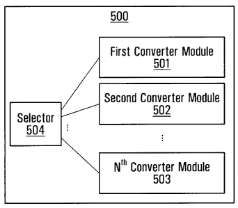
Referring now to Figure 5, shown is a block diagram of a DCDC
converter 500 featuring a plurality of converter modules 501,502,503. Each
converter
module 501,502,503 is configured to convert current at a first voltage level
to another
voltage form. In some implementations, there is a filter (not shown) at the
output for
reducing ripple effects of PWM in order to achieve a smoother analog output.
[0038] In
some implementations, each converter module 501,502,503 has at
least one switch configured to convert the current using PWM. The switch might
for
example be a pair of transistors as will be shown in subsequent examples. More
generally, each converter module 501,502,503 has any appropriately configured
switch used to convert the current using PWM.
[0039]
Switching the switches on and off introduces internal power losses for
example because of capacitances inherent with the switches. Under low load
conditions when current draw from any circuits being powered by the DCDC
converter 500 is relatively low, the DCDC converter 500 does not deliver much
power
but might still have substantially the same internal power losses from the
switching.
Therefore, inefficiencies can be relatively large if all of the switches are
being switched
on and off under low load conditions.
[0040] In
accordance with an embodiment of the disclosure, the converter
modules 501,502,503 are configured to be dynamically enabled or disabled such
that
only each converter module 501,502,503 that has been enabled converts current
for
an output of the DCDC converter 500. Any
switches of the converter
modules 501,502,503 that have been disabled do not get switched on and off.
Therefore, any inefficiency that would have been introduced by those switches
are
mitigated or eliminated altogether. The effect is that efficiency can be
improved during
low load conditions when there is no need to enable all of the converter
modules 501,502,503.
[0041] In
some implementations, as shown in the illustrated example, the
DCDC converter 500 has a selector 504. The selector is configured to
dynamically
enable or disable the converter modules 501,502,503 based on loading
conditions. In
CA 02801586 2013-01-10
41527-CA-PAT =
- 12 -
the event that the DCDC converter 500 experiences low load conditions, then
the
selector 504 disables some of the converter modules 501,502,503. Conversely,
in the
event that the DCDC converter 500 experiences higher load conditions, then the
selector 504 enables more of the converter modules 501,502,503. By dynamically
enabling or disabling the converter modules 501,502,503 based on loading
conditions,
efficiency can be improved during low load conditions.
[0042] In
alternative implementations, the converter modules 501,502,503 are
implemented in an apparatus without any selector being present. The apparatus
might for example be an integrated circuit configured to receive enable
signals in
order to dynamically enable or disable the converter modules 501,502,503.
Other
implementations are possible.
[0043] In
some implementations, the dynamic enabling/disabling of the
converter modulet 501,502,503 modules means that the DCDC converter 500 as a
whole need not perform the same way all of the time. This is because the
converter
modules 501,502,503 can be put into use or out of use, without (colloquially
speaking)
any actual re-wiring of the hardware. Instead, electrical control signals can
bring a
converter module into play or out of play and thereby change performance. In
some
implementations, this is performed dynamically based on loading conditions.
[0044] In
some implementations, the converter modules 501,502,503 are
provided in parallel. This
enables the converter modules 501,502,503 to be
individually controllable with independent control. Further details of how
converter
modules might be individually controllable are provided below with reference
to
Figure 6.
[0045]
Referring now to Figure 6, shown is a block diagram of another DCDC
converter 600 featuring a plurality of converter modules 601,602,603. Each
converter
module 601,602,603 has a switch 613,614 configured to convert current at a
first
voltage level VB,477 to another voltage form according to a PWM signal
provided by a
PWM module 605 using the energy stored in the inductor. In some
implementations,
there is a filter 606,609 at the output for reducing ripple effects of PWM in
order to
achieve a smoother analog output. In the illustrated example, the filter
606,609
includes an inductor 606 to smooth current passing through it, and a capacitor
609 for
CA 02801586 2013-01-10
41527-CA-PAT
=
- 13 -
reducing ripple content in voltage caused by PWM. More generally, any
appropriately
configured filter can be implemented.
[0046] In
the illustrated example, the switch 613,614 includes a P-channel
FET 613 configured to periodically connect the first voltage level 14,477 to
the
filter 606,609 according to the PWM signal. The switch 613,614 also includes
an N-
channel FET configured to connect a ground voltage to the filter 606,609
whenever
the P-channel FET 613 has not connected the first voltage level VBATT to the
filter 606,609. Other switches are possible. More generally, any appropriately
configured switch can be implemented for converting current at the first
voltage level
VBATT to another voltage form.
[0047]
Switching the transistors 613,614 on and off introduces internal power
losses for example because of capacitances inherent with the transistors
613,614.
Under low load conditions when current draw from any circuits being powered by
the
DCDC converter 600 is relatively low, the DCDC converter 600 does not deliver
much
power but might still have substantially the same internal power losses from
the
switching.
Therefore, inefficiencies can be relatively large if all of the
transistors 613,614 are being switched on and off under low load conditions.
[0048] In
accordance with an embodiment of the disclosure, each converter
module 601,602,603 has logic circuitry 610,611,612 configured to provide the
PWM
signal to its switch 613,614 only if the converter module 601,602,603 has been
enabled. The transistors 613,614 of the converter modules 601,602,603 that
have
been disabled are off. Therefore, any inefficiency that would have been
introduced by
those transistors 613,614 are mitigated or eliminated altogether. The effect
is that
efficiency can be improved during low load conditions when there is no need to
enable
all of the converter modules 601,602,603.
[0049] In
some implementations, the switches 613,614 and the logic
circuitry 610,611,612 are distributed to form a bus.
Each converter
module 601,602,603 is individually controllable with an independent control
line that is
controlled digitally. To this end, each converter module 601,602,603 receives
a
respective enable signal en(1),en(2),en(N) from a processor 604 for
selectively
enabling or disabling the converter module 601,602,603.
CA 02801586 2013-01-10
41527-CA-PAT
- 14 -
[0050] In some implementations, as shown in the illustrated example,
each
converter module 601,602,603 includes an inverter 610 and a NAND gate 611
configured to drive the P-channel FET 613 with the PWM signal only if the
enable
signal en(1),en(2),en(N) for the converter module 601,602,603 has been set to
high;
otherwise, the P-channel FET 613 is off. In some implementations, as shown in
the
illustrated example, each converter module 601,602,603 includes an AND gate
612
configured to drive the N-channel FET 614 with the PWM signal only if the
enable
signal en(1),en(2),en(N) for the converter module 601,602,603 has been set to
high;
otherwise, the N-channel FET 614 is off.
[0051] By way of example, if the processor 604 is to enable the first
converter
module 601, then the processor 604 sets the enable signal en(1) for the first
converter
module 601 to high. The effect is that the output of the NAND gate 611 is
equal to the
PWM signal and therefore the P-channel FET 613 is driven by the PWM signal.
Furthermore, the output of the AND gate 612 is also equal to the PWM signal
and
therefore the N-channel FET 614 is driven by the PWM signal. Therefore, the
switch 613,614 is driven by the PWM signal when the first converter module 601
has
been enabled.
[0052] Conversely, if the processor 604 is to disable the first
converter
module 601, then the processor 604 sets the enable signal en(1) to low. The
effect is
that the output of the NAND gate 611 is high and therefore the P-channel FET
613 is
turned off. Furthermore, the output of the AND gate 612 is low and therefore
the N-
channel FET 614 is turned off. Therefore, the switch 613,614 is turned off and
is not
driven by the PWM signal when the first converter module 601 has been
disabled.
[0053] It is to be understood that there are alternative possibilities
for the logic
circuitry 610,611,612. Any suitable logic circuitry that drives the switch
613,614 with
the PWM signal only when the converter module 601,602,603 has been enabled can
be implemented. Note that this might not necessarily involve the inverter 610,
the
NAND gate 611, and the AND gate 612. In alternative implementations, each
converter module 601,602,603 receives two separate enable signals: a first
enable
signal for enabling the P-channel FET 613, and a second enable signal for
enabling
the N-Channel FET 614. For example, the two separate enable signals can be
directly generated inside the PWM module 605 for each converter
CA 02801586 2013-01-10
41527-CA-PAT
- 15 -
module 601,602,603 using other gates. Other implementations are possible that
provide the same functionality of turning the P-channel FET 613 on while the N-
channel FET 614 is off, and P-channel FET 613 off while the N-channel FET 614
is
turned on, and providing an enable signal that enables this operation. When
the
enable is turned off, both devices are turned off.
[0054] The processor 604 is configured to dynamically enable or
disable the
converter modules 601,602,603 based on loading conditions. In the event that
the
DCDC converter 600 experiences low load conditions, then the processor 604
disables some of the converter modules 601,602,603. Conversely, in the event
that
the DCDC converter 600 experiences higher load conditions, then the processor
604
enables more of the converter modules 601,602,603. By dynamically enabling or
disabling the converter modules 601,602,603 based on loading conditions,
efficiency
can be improved during low load conditions. In many cases, the processor 604
can
be provided with knowledge to increase the output. For example, if the DCDC
converter 600 is implemented in a wireless handset and the processor 604 is to
turn
on more load or a DSP processor sends a request to a transceiver to increase
output
power, then such information can be provided to the processor 604 to control
the
converter modules 601,602,603 accordingly.
[0055] In some implementations, the processor 604 is configured to
implement
the dynamic selection of converter modules 601,602,603 according to software
operating on the processor 604. For such implementations, the DCDC converter
600
is implemented in an apparatus having the processor 604 and a memory (not
shown)
having stored thereon computer-executable instructions that when executed on
the
processor 604 implement a method for performing the dynamic selection. Further
details of the method for performing the dynamic selection are provided below
with
reference to Figure 10.
[0056] In alternative implementations, software is not utilised to
implement the
dynamic selection of converter modules 601,602,603. Instead, the dynamic
selection
of converter modules 601,602,603 is implemented with only hardware and/or
firmware. For example, control can be exerted by an on chip processing element
(e.g.
a state machine or other simple processor). More generally, the dynamic
selection of
CA 02801586 2013-01-10
41527-CA-PAT
- 16 -
converter modules 601,602,603 can be implemented using software, firmware,
hardware, or any appropriate combination thereof.
[0057] In
other alternative implementations, the dynamic selection of converter
modules 601,602,603 is implemented by an external component. For example, the
DCDC converter 600 might be implemented in an integrated circuit having an
interface
for receiving the dynamic selection via external control. The interface might
for
example be a serial interface or other interface. More generally, the dynamic
selection of converter modules 601,602,603 can be implemented with the DCDC
converter 600 or externally.
[0058] Each
converter module 601,602,603 that has been enabled converts
current at the first voltage level VBATT to another voltage form, which is
then filtered by
the filter 606,609 in order to generate a filtered output voltage as similarly
described
with reference to Figure 1. Therefore, the current
'load provided to any circuits being
powered by the DCDC converter 600 is provided at the filtered output voltage.
The
magnitude of the filtered output voltage is determined based on a duty cycle
of the
PWM signal. In some implementations, as shown in the illustrated example, the
duty
cycle of the PWM signal is determined based on a reference voltage Vref
provided to
the PWM module 605.
[0059] In
some implementations, as shown in the illustrated example, the
DCDC converter 600 has a feedback loop so that the duty cycle of the PWM
signal
can be adjusted in order to hold the filtered output voltage at the output.
The
feedback voltage Vfb is equal to the filtered output voltage multiplied by a
ratio of a pair
of resistors 607,608. If the feedback voltage Vfb is less than the reference
voltage Vref,
then the PWM module 605 increases the duty cycle. Conversely, if the feedback
voltage Vfb is greater than the reference voltage Vref, then the PWM module
605
decreases the duty cycle.
[0060] In
some implementations, the filtered output voltage can be controlled by
controlling the ratio of the pair of resistors 607,608 while keeping Vref
constant (e.g.
internally generate Vref). Alternatively, the filtered output voltage can be
controlled by
keeping the pair of resistors 607,608 constant (e.g. internally implemented
resistors)
and varying Vref.
CA 02801586 2013-01-10
41527-CA-PAT =
- 17 -
[0061] In some implementations, as shown in the illustrated example,
the
DCDC converter 600 includes a power transistor 615 configured to supply the
first
voltage level VBATT to the filter 606,609 at the output in response to a
bypass enable
signal ben provided by the processor 604. Note that the power transistor 615
is not a
converter module because it does not convert current from the first voltage
level VBATT
to another voltage form. The power transistor 615 can be used to bypass the
converter modules 601,602,603 when it is desired to supply current at the
first voltage
level VBATT while avoiding any inefficiencies introduced by the converter
modules 601,602,603 and while enabling open loop control. Alternatively, the
power
transistor 615 can be used to supplement current provided by the converter
modules 601,602,603.
[0062] In some implementations, when highest output power is desired,
the
power transistor 615 is turned on. As output power drops slightly, the power
transistor 615 can be turned off while all converter modules 601,602,603 are
enabled
by setting all of the enable signals en(1),en(2),en(N) to high. As demand for
output
power further decreases, some of the enable signals en(1),en(2),en(N) can be
set to
low in order to disable some of the converter modules 601,602,603 in order to
reduce
conduction and driver losses thereby improving efficiency.
[0063] Whilst the DCDC converter 600 uses PWM, it is to be understood
that
this does not preclude use of PFM for any drive condition. PFM implementations
are
possible and are within the scope of the disclosure. Furthermore, whilst the
DCDC
converter 600 focuses on using one power phase, it is to be understood that
this does
not preclude use of multiple power phases. Using multiple power phases can
help to
reduce ripples on the output. Multiple power phase implementations are
possible and
are within the scope of the disclosure.
[0064] Referring now to Figure 7, shown is a block diagram of another
DCDC
converter 700 featuring a plurality of converter modules 701,702,703. The DCDC
converter 700 also has a filter 706,709 for filtering ripples caused by PWM, a
pair of
resistors 707,708 for a feedback loop, and a power transistor 715 supplying
current at
the first voltage level 1/23,477. The converter modules 701,702,703, the
filter 706,709,
the resistors 707,708, and the power transistor 715 substantially correspond
to
CA 02801586 2013-01-10
41527-CA-PAT =
- 18 -
components already described above with reference to Figure 6 and therefore
details
are not repeated here.
[0065] The
processor 704 dynamically enables or disables the converter
modules 701,702,703 as similarly described above with reference to Figure 6.
However, in contrast with the processor 604 described above with reference to
Figure 6, the processor 704 also generates the PWM signal sw based on a
reference
voltage Võf. Therefore, the DCDC converter 700 does not use a separate PWM
module. Furthermore, if the reference voltage lire is digitized, then there is
no need
for an external digital to analog converter to provide the reference voltage
Võf to a
PWM module.
[0066] In
some implementations, as shown in the illustrated example, the
DCDC converter 700 also has a feedback loop so that the duty cycle of the PWM
signal can be adjusted in order to hold a voltage level at the output.
However, in
contrast with the DCDC converter 600 shown in Figure 6, the feedback loop goes
back to the processor 704. In the illustrated example the processor 704 is a
digital
processor and therefore there is provided an analog to digital converter 705
configured to convert the feedback voltage Vfb into digital form.
[0067] In
alternative implementations, a comparator can be used to compare
the reference voltage Võf with the feedback voltage Vfb in order to generate
an error
signal when the feedback voltage Vfb drops below the reference voltage Võf.
Figure 8
depicts such a comparator 800 in which a single bit digitized error signal can
be
generated for a processor/controller. Such error signal could be provided to
the
processor 704 shown in Figure 7 so that the processor 704 can adjust the duty
signal
of the PWM signal according to the error signal.
Multiple DCDC Converters
[0068]
Referring now to Figure 9, shown is a block diagram of an
apparatus 900 having multiple DCDC converters 901,902,903. Multiple DCDC
converters 901,902,903 can be implemented for example when it is desired to
have
multiple different voltage levels for powering different circuits. The
DCDC
CA 02801586 2013-01-10
41527-CA-PAT
- 19 -
converters 901,902,903 are substantially identical to the DCDC converter 700
shown
in Figure 7 and therefore details are not repeated here.
[0069] The
DCDC converters 901,902,903 are controlled by a single
programmable controller, namely a processor 904. The processor 904 processes
multiple feedback signals through multiple analog to digital converters and
generates
the PWM signal sw as well as the enable signals en(1),en(2),en(N) as similarly
described in the previous examples.
[0070] In
the illustrated example, there are multiple analog to digital converters
(i.e. one analog to digital converter per DCDC converters 901,902,903). In
alternative
implementations, a single multi-channel analog to digital converter is used.
All of the
feedback signals can be converted using the single multi-channel analog to
digital
converter. This can potentially reduce hardware cost.
[0071] In
the illustrated example, each DCDC converter 901,902,903 is shown
to have a closed loop. However, closed loop regulation can be converted to
open
loop regulation when loads are expected to stay static. Hence, the analog to
digital
conversion can be duty cycled to reduce power under light load/stand-by
conditions.
Method of Dynamic Selection
[0072]
Referring now to Figure 10, shown is a flowchart of a method for
performing dynamic selection of converter modules.
This method can be
implemented by an apparatus, for example by the selector 504 of the DCDC
converter 500 shown in Figure 5, the processor 604 of the DCDC converter 600
shown in Figure 6, the processor 704 of the DCDC converter 700 shown in Figure
7,
or the processor 904 of the apparatus 900 shown in Figure 9. More generally,
this
method can be implemented by any appropriately configured apparatus comprising
a
DCDC converter having a plurality of converter modules each configured to
convert
current from a first voltage level to another level.
[0073] At
step 10-1, the apparatus determines on an ongoing basis an
estimated total power usage for at least one circuit being powered by the DCDC
converter. At step 10-2, the apparatus determines which converter modules to
enable
and which converter modules to disable based on the estimated total power
usage.
CA 02801586 2013-01-10
41527-CA-PAT
- 20 -
Finally, at step 10-3, the apparatus dynamically enables or disables the
converter
modules accordingly.
[0074]
There are many ways that the apparatus can determine the estimated
power usage. In some implementations, the apparatus maintains a look-up table
that
identifies, for each circuit, power usage as a function of operation of the
circuit. For
each circuit, the apparatus determines an operating state and a resulting
power usage
according to the look-up table. Therefore, the apparatus can determine the
estimated
total power usage as a sum of all resulting power usages determined from the
look-up
table.
[0075] By way of example, if the at least one circuit being powered by the
DCDC converter includes a wireless access radio, then the look-up table might
identify a first power usage for when the wireless access radio is idle and a
second
power usage for when the wireless access radio is actively
transmitting/receiving. The
apparatus determines whether the wireless access radio is idle or is actively
transmitting/receiving, and then determines a resulting power usage according
to the
look-up table. If there are other circuits being powered by the DCDC
converter, then
the apparatus determines for each circuit an operating state and a resulting
power
usage according to the look-up table. Finally, the apparatus determines the
estimated
total power usage as a sum of all resulting power usages determined from the
look-up
table.
[0076]
There are many ways that the apparatus can determine which converter
modules to enable and which converter modules to disable. In
some
implementations, the apparatus determines a minimum number of converter
modules
that should be enabled in order to handle the estimated total power usage.
Therefore,
the apparatus can determine which converter modules to enable and which
converter
modules to disable in accordance with the minimum number of converter modules
that
should be enabled.
[0077] By
way of example, if each converter module is capable of supplying
500mW of power and the estimated total power usage is 3.3W, then at least
seven
converter modules should be enabled. If five converter modules are already
enabled,
then the apparatus might enable another two converter modules so that a total
of
CA 02801586 2013-01-10
41527-CA-PAT
- 21 -
seven converter modules are enabled. If ten converter modules are already
enabled,
then the apparatus might disable three of these converter modules so that a
total of
seven converter modules are enabled. If each converter module is identical,
then the
selection is arbitrary.
[0078] In alternative implementations, the converter modules are not
identical
and therefore the apparatus takes this into account when determining which
converter
modules to enable and which converter modules to disable. By way of example,
the
converter modules might include a mix of different converter modules capable
of
supplying 500mW, 1000mW, or 3000mW of power. If the estimated total power
usage
is 3.3W, then the apparatus might enable one of the converter modules capable
of
supplying 3000mW of power and one of the converter modules capable of
supplying
500mW. Note that this might be more efficient than enabling two of the
converter
modules capable of supplying 3000mW of power. The converter modules capable of
supplying more power might have larger switches and therefore more internal
power
losses for example because of capacitances inherent with the switches.
Computer Readable Medium
[0079] In accordance with another embodiment of the disclosure, there
is
provided a non-transitory computer readable medium having computer executable
instructions stored thereon for execution on a processor of an apparatus so as
to
implement the method described above. The non-transitory computer readable
medium might for example be an optical disk such as a Compact Disk (CD), a
Digital
Video Disk (DVD), or a Blu-Ray Disk (BD). Alternatively, the non-transitory
computer
readable medium might for example be a memory stick, a memory card, a disk
drive,
a solid state drive, etc. Other non-transitory computer readable media are
possible
and are within the scope of this disclosure. More generally, the non-
transitory
computer readable medium can be any tangible medium in which the computer
executable instructions can be stored.
Mobile Device
[0080] Referring now to Figure 11, shown is a block diagram of a
mobile
device 1100. This mobile device 1100 is presented as an example apparatus that
CA 02801586 2013-01-10
41527-CA-PAT =
- 22 -
might implement a DCDC converter with converter modules that can be
dynamically
enabled or disabled based on loading condition of various circuits the within
mobile
device 1100.
[0081] The
mobile device 1100 has a many circuits as will be described in
further detail below. Some or all of these circuits can be powered using the
DCDC
converter 500 shown in Figure 5, the DCDC converter 600 shown in Figure 6, or
the
DCDC converter 700 shown in Figure 7. In some implementations, multiple DCDC
converters are used in order to power the circuits as similarly described
above with
reference to Figure 9. In some implementations, one or more DCDC converters
can
work in concert with or supplant other power-management systems or techniques,
etc.
[0082] It
is to be understood that the mobile device 1100 is shown with very
specific details and is provided only as an example. Other mobile devices are
possible and are within the scope of this disclosure. Furthermore, other
apparatuses
(e.g. desktop computer, tablet computer, etc.) are possible, whether mobile or
not,
and are within the scope of this disclosure. In other words, embodiments of
the
disclosure are applicable to a variety of devices and uses, including devices
that are
not mobile devices.
[0083] The
mobile device 1100 has a housing that may be elongated vertically,
or may take on other sizes and shapes (including clamshell housing
structures). The
keyboard 1114 may include a mode selection key, or other hardware or software
for
switching between text entry and telephony entry.
Alternatively, the mobile
device 1100 may have a housing that does not take on other sizes and shapes.
[0084]
Size and weight of any DCDC converters in the mobile device 1100 can
be important design considerations. In some implementations, each DCDC
converter
is made to be small and lightweight, which can be advantageous for handheld
devices
such as the mobile device 1100 which is sized and shaped to be held or carried
in a
human hand. Note that for alternative non-mobile embodiments, size and weight
of
any DCDC converters might be of lesser importance.
[0085] A
microprocessor 1128 is shown schematically as coupled between a
keyboard 1114 and a display 1126. The microprocessor 1128 is a type of
processor.
CA 02801586 2013-01-10
41527-CA-PAT
=
- 23 -
The microprocessor 1128 controls operation of the display 1126, as well as
overall
operation of the mobile device 1100, in response to actuation of keys on the
keyboard 1114 by a user.
[0086] In
addition to the microprocessor 1128, other parts of the mobile
device 1100 are shown schematically. These include: a communications
subsystem 1170; a short-range communications subsystem 1102; the keyboard 1114
and the display 1126, along with other input/output devices including a set of
LEDs 1104, a set of auxiliary I/0 devices 1106, a serial port 1108, a speaker
1111 and
a microphone 1112; as well as memory devices including a flash memory 1116 and
a
Random Access Memory (RAM) 1118; and various other device subsystems 1120.
The mobile device 1100 may have a battery 1121 to power the active elements of
the
mobile device 1100. The mobile device 1100 is in some embodiments a two-way
radio frequency (RF) communication device having voice and data communication
capabilities. In addition, the mobile device 1100 in some embodiments has the
capability to communicate with other computer systems via the Internet.
[0087]
Operating system software executed by the microprocessor 1128 is in
some embodiments stored in a persistent store, such as the flash memory 1116,
but
may be stored in other types of memory devices, such as a read only memory
(ROM)
or similar storage element. In addition, system software, specific device
applications,
or parts thereof, may be temporarily loaded into a volatile store, such as the
RAM 1118. Communication signals received by the mobile device 1100 may also be
stored to the RAM 1118.
[0088] The
microprocessor 1128, in addition to its operating system functions,
enables execution of software applications on the mobile device 1100. A
predetermined set of software applications that control basic device
operations, such
as a voice communications module 1130A and a data communications
module 1130B, may be installed on the mobile device 1100 during manufacture.
In
addition, a personal information manager (PIM) application module 1130C may
also
be installed on the mobile device 1100 during manufacture. The PIM application
is in
some embodiments capable of organizing and managing data items, such as e-
mail,
calendar events, voice mails, appointments, and task items. The PIM
application is
also in some embodiments capable of sending and receiving data items via a
wireless
CA 02801586 2013-01-10
41527-CA-PAT =
- 24 -
network 1110. In some embodiments, the data items managed by the PIM
application
are seamlessly integrated, synchronized and updated via the wireless network
1110
with the device user's corresponding data items stored or associated with a
host
computer system. Additional software modules, illustrated as another software
module 1130N, may be installed during manufacture.
[0089] Communication functions, including data and voice
communications, are
performed through the communication subsystem 1170, and possibly through the
short-range communications subsystem 1102. The communication subsystem 1170
includes a receiver 1150, a transmitter 1152, a GPS receiver 1162, and one or
more
antennas, illustrated as a receive antenna 1154, a transmit antenna 1156, and
a GPS
antenna 1164. In addition, the communication subsystem 1170 also includes a
processing module, such as a digital signal processor (DSP) 1158, and local
oscillators (L0s) 1160.
[0090] The specific design and implementation of the communication
subsystem 1170 might be dependent upon the communication network in which the
mobile device 1100 is intended to operate. The communication network might be
a
cellular network. For example, the communication subsystem 1170 of the mobile
device 1100 may be designed to operate with the MobitexTM, DataTACTm or
General
Packet Radio Service (GPRS) mobile data communication networks and also
designed to operate with any of a variety of voice communication networks,
such as
Advanced Mobile Phone Service (AMPS), Time Division Multiple Access (TDMA),
Code Division Multiple Access (CDMA), Personal Communications Service (PCS),
Global System for Mobile Communications (GSM), etc. Examples of CDMA include
1X and lx EV-DO, and Wideband CDMA. Other applicable communication networks
might include packet data systems, Enhanced Data rates for GSM Evolution
(EDGE),
E-EDGE, UMTS/UTRAN, OFDMA systems, TD-SCDMA systems, LTE/E-UTRAN, etc.
The communication subsystem 1170 may also be designed to operate with a non-
cellular network such as an 802.11 Wi-Fi network or an 802.16 WiMAX network or
both. Other types of data and voice networks, both separate and integrated,
may also
be utilized with the mobile device 1100.
[0091] Network access may vary depending upon the type of
communication
system. For example, in the MobitexTM and DataTACTm networks, mobile devices
are
CA 02801586 2013-01-10
41527-CA-PAT
- 25 -
registered on the network using a unique Personal Identification Number (PIN)
associated with each device. In GPRS networks, however, network access is
typically
associated with a subscriber or user of a device. A GPRS device therefore
typically
has a subscriber identity module, commonly referred to as a Subscriber
Identity
Module (SIM) card, in order to operate on a GPRS network.
[0092] When network registration or activation procedures have been
completed, the mobile device 1100 may send and receive communication signals
over
the communication network 1110. Signals received from the communication
network 1110 by the receive antenna 1154 are routed to the receiver 1150,
which
provides for signal amplification, frequency down conversion, filtering,
channel
selection, etc., and may also provide analog to digital conversion. Analog-to-
digital
conversion of the received signal allows the DSP 1158 to perform more complex
communication functions, such as demodulation and decoding. In a similar
manner,
signals to be transmitted to the network 1110 are processed (e.g., modulated
and
encoded) by the DSP 1158 and are then provided to the transmitter 1152 for
digital to
analog conversion, frequency up conversion, filtering, amplification and
transmission
to the communication network 1110 (or networks) via the transmit antenna 1156.
[0093] In addition to processing communication signals, the DSP 1158
provides
for control of the receiver 1150, the transmitter 1152, and the GPS receiver
1162. For
example, gains applied to communication signals in the receiver 1150 and the
transmitter 1152 may be adaptively controlled through automatic gain control
algorithms implemented in the DSP 1158.
[0094] In a data communication mode, a received signal, such as a text
message or web page download, is processed by the communication subsystem 1170
and is input to the microprocessor 1128. The received signal is then further
processed by the microprocessor 1128 for an output to the display 1126, or
alternatively to some other auxiliary I/0 devices 1106. A device user may also
compose data items, such as e-mail messages, using the keyboard 1114 or some
other auxiliary I/0 device 1106, such as a touchpad, a rocker switch, a thumb-
wheel,
or some other type of input device, or combinations thereof. The composed data
items may then be transmitted over the communication network 1110 via the
communication subsystem 1170.
CA 02801586 2013-01-10
41527-CA-PAT
- 26 -
[0095] In a voice
communication mode, overall operation of the device is
substantially similar to the data communication mode, except that received
signals are
output to a speaker 1111, and signals for transmission are generated by a
microphone 1112. Alternative voice or audio I/0 subsystems, such as a voice
message recording subsystem, may also be implemented on the mobile device
1100.
In addition, the display 1126 may also be utilized in voice communication
mode, for
example, to display the identity of a calling party, the duration of a voice
call, or other
voice call related information.
[0096] Location
determination using GPS technology involves receiving GPS
signals from GPS
satellites 1166 on the antenna 1164. The GPS signals are received
using the GPS receiver 1162 and processed by the DSP 1158. Typically, GPS
signals from at least four satellites are processed. Further details of GPS
are omitted
for simplicity.
[0097] The short-
range communications subsystem 1102 enables
communication between the mobile device 1100 and other proximate systems or
devices, which need not necessarily be similar devices. For example, the short
range
communications subsystem may include an infrared device and associated
circuits
and components, or a BluetoothTM communication module to provide for
communication with similarly-enabled systems and devices.
[0098] Numerous
modifications and variations of the present disclosure are
possible in light of the above teachings. It is therefore to be understood
that within the
scope of the appended claims, the disclosure may be practised otherwise than
as
specifically described herein.