Note: Descriptions are shown in the official language in which they were submitted.
CA 02801948 2012-12-07
WO 2011/153606
PCT/CA2010/000864
ORTHOMODE TRANSDUCER
Field of the Invention
The present invention relates in general to radiofrequency electromagnetic
waveguide devices for polarization mode separation or recombination and, in
particular,
to an OMT design that is easy to fabricate and assemble with high precision,
and can be
scaled for frequencies above 30 GHz to at least 500 GHz.
Background of the Invention
A well known problem in radiofrequency (RF) astronomy is how to separately
investigate both polarization modes from a RF source. Orthomode transducers
(OMTs)
are used to de-diplex incident electromagnetic (EM) radiation. In many other
applications
there is need for polarization diplexers and de-diplexers. Generally low
return loss, high
isolation and low cross-polarization OMTs are desired. While it is also
generally desirable
to reduce insertion loss, this loss is mostly attributed to conduction losses
within the
waveguide structure, and so is principally determined by the materials, and
less so by the
design, and are rather small. As return loss, cross-polarization and isolation
depend on
wavelength, there is a need for OMTs that provide acceptable quality in each
respect
over an intended operating range. In some cases the operating range is narrow
band,
but in many cases the broader the band the better. All OMTs are trade-offs in
these
features along with costs of production and assembly, and reliable operation.
A chief component of OMTs that can be used to classify them is the (principal)
junction, which connects a polarization diplexed waveguide with at least 2
paths. Some
OMT designs use a turnstile junction while other OMT designs use Boifot
junctions or
double ridge junctions.
The Boifot junction is a relatively complex device that requires two pins and
a
septum (three matching elements) or an iris to be positioned within the
waveguide.
Features such as the matching pins, septum, or iris, increase return loss,
increase an
expense of the device, complicate assembly, limit the bandwidth over which the
OMT
operates, and limits the smallest size the OMT can obtain (and/or the
fabrication
techniques that can be employed to produce them), limiting low cost production
of higher
frequency band OMTs. Higher frequency OMTs require smaller devices, and
greater
accuracy of the definition of the matching elements, which is increasingly
difficult to
1
CA 02801948 2012-12-07
WO 2011/153606
PCT/CA2010/000864
produce. Moreover, the septum is a mobile piece and the return losses of the
OMTs are
therefore prone to change when the septum is moved out of alignment.
There are several commonalities between the Boifot and double ridge OMT
structures. In both cases, two arms are fundamentally different: one arm is
provided by a
pair of (initially oppositely directed) waveguides that are subsequently
reunited, and the
other arm is never divided. The double ridge design also requires intricate
features (on
both sides of the waveguide) that are also more difficult and expensive to
produce and
assemble, and increasingly so at smaller scales (higher frequencies). As
matching
features have to be provided on two or more parts and as there are very low-
tolerances
for the alignment of these features, it is unsurprising that these designs
fail to produce
high quality OMTs with good repeatability, especially at higher frequencies
(i.e. above 30
GHz).
For example, Double-Ridged OMT (Shin'iciro Asayama National Astronomical
Observatory of Japan) according to which ridges are provided from above and
below an
input waveguide shows a design that is, in principle, scalable to smaller
dimensions and
higher frequencies. While 7 examples were produced and all have apparently the
similar
reflection losses, cross-polarization over the band from 110-170 GHz varies
from -24 to -
40 dB depending on the example, and over ALMA band 4, varies from -28 to -42
dB.
Having matching elements produced on multiple parts complicates production and
assembly and leads to small errors that can affect reproducibility and/or
quality of the
OMT. The problems with repeatability may be caused by the fact that the
matching
elements are provided in multiple parts.
A turnstile junction is a waveguide network with a diplexed waveguide port (+z
axis) and two paired perpendicular waveguide paths (+,- x axis, and +,- y
axis). A
matching (or tuning) element (or feature having one or more elements) is
provided at the
origin where these waveguide paths meet, opposite the diplexed waveguide port.
To
produce an OMT, the oppositely directed pairs of waveguide paths are made to
recombine after traveling equal electrical path lengths, and the recombined
paths
communicate with respective ports. Thus there are three ports, one for s-
polarized
signal, one for p-polarized signal, and one for the diplexed signal.
Various matching features are known for turnstile junctions, including a
trunked
pyramid (as used by Navarrini et at. described below), and concentric cylinder
matching
stubs (e.g. M. A. Meyer et at. entitled "Applications of the Turnstile
Junction" IRE-
Transactions on Microwave Theory and Technique pp.40-45, Dec.1955).
2
CA 02801948 2012-12-07
WO 2011/153606
PCT/CA2010/000864
Among the OMT literature surveyed by the Applicant, there was only one device
that was able to offer very good cross-polarization and isolation. It was
taught by
Navarrini et al. in "A Turnstile Junction Waveguide Orthomode Transducer" IEEE
Transactions on Microwave Theory and Technique, v.54, Not 2006. The OMT was
designed for the 18-26 GHz frequency range, and across this range, the
insertion loss
was 0.15 dB, and the cross-polarization was less than -47 dB for both
polarizations.
While it may be desirable to improve on the return loss of (-19 dB), it
represents a major
improvement over the available alternatives. The model of this OMT includes
one 180
bend for each of the 4 waveguide paths from the turnstile so that the paired
waveguide
paths are convergent, and the pairs are then coupled by E-plane Y power
combiners.
The OMT is divided into 4 parts that are assembled as 4 quarters, each having
an edge
that meet along a center axis that passes through the center of the diplexed
waveguide.
When Navarrini (Test of 1 mm Band Turnstile Junction Waveguide Orthormode
Transducer, 17th mt. Symp. on Space Terahertz Technology P1-21) attempted to
miniaturize the same design, to produce an OMT for use in the 200-270GHz
frequency
range, the transmission loss was 0.8 dB, the return loss was -12 dB and the
cross-
polarization was lower than -25 dB for both polarizations. This device is not
nearly as
successful as the 18-26 GHz frequency range device.
There are other OMT designs known in the art that use a turnstile junction
with
matching feature as the principle divider. Some are appreciated for their
compactness,
and low part count, but deliver (or even fail to deliver) marginal quality
polarization
diplexing or de-diplexing, i.e. return loss, cross-polarization and isolation
from -20 to -25
dB, even over lower bandwidths. The low quality of the many known turnstile-
based OMT
designs, Navarinni's first design excluded, and the non-scalability of
Navarrini's device
would lead research away from this design. Some examples of low quality
turnstile-type
OMT designs and their noted features include US 7,397,323 to Hozouri and a
paper to
Aramaki et al. entitled "Ultra-Thin Broadband OMT with Turnstile Junction"
(also patented
US 7,330,088 and US 7,019,603).
US 7,397,323 to Hozouri teaches a waveguide orthomode transducer having at a
first layer, a turnstile junction having a main waveguide and four waveguide
ports, each
coupled to a respective magic-T with an E-port, two opposed side-ports, and an
H-port.
The magic-Ts (called therein hybrid Ts) are ring-arranged around the turnstile
junction so
the waveguide ports each communicate with one H-port, so adjacent magic-Ts
inter
communicate with their respective side-ports, and so the E-ports form two sets
of
opposed E-ports. In a second layer two H-plane power dividers/combiners each
have an
3
CA 02801948 2012-12-07
WO 2011/153606
PCT/CA2010/000864
axial-port and two opposed side-ports. The H-plane power dividers/combiners
are
arranged so their respective side-ports communicate with different ones of the
two sets of
opposed E-ports and so their axial-ports are polarization ports. This permits
a single
signal with two fundamental orthogonally polarized modes to enter the main
waveguide
and exit separated at the polarization ports, and vice versa.
This design is stated to be advantageous in that it provides a compact and
thin
waveguide OMT, and that it is easy to manufacture, however no explanation as
to how it
would be manufactured is taught or suggested. Furthermore, no example is
provided,
and no data regarding signal power, isolation, mode purity, bandwidth, voltage
standing
wave ratio, or any other feature (except profile height, which is not
supported by any
simulation or other data).
In any case, the ring coupling of the 4 turnstile arms is expected not to
provide low
return loss, isolation, or low cross-polarization, because of the use of magic-
T junctions.
Magic-T couplers typically have theoretical return losses of about -20 dB over
a 22.4%
bandwidth (-30 dB minimum at a point), if the magic-T is properly matched (in
this case
with an inductive post), and is never better than about -5 dB without the
matching
element. FIG. 1 is a graph showing simulated return losses for a magic-T
coupler, with
and without an inductive post matching feature. It will be noted that
unmatched magic-Ts
have high return losses that constitute impermissible losses in many
applications.
Furthermore these losses can result in standing waves that lead to internal
arcing, which
must be avoided, for example, by limiting a power the OMT can handle safely.
Matching
features (inductive post, iris, reflectors or matching screws) can be added to
the magic-T
to reduce reflection losses. Such matching features are typically expensive
to
manufacture or position, and, while they may significantly reduce return
losses
(reflection), this improved loss is typically over a narrow bandwidth. The
inclusion of
these elements must be precisely aligned. As they are formed on different
planes of
different parts, this complicates alignment within required prescision.
Furthermore these
features also limit the power the OMT can safely diplex/de-diplex. Hozouri
does not
mention any matching element, without which the device has a theoretically
optimal
return loss of about -5 dB.
In Hozouri's example, each magic-T junction is used twice. The magic-T is
first
used as a (polarization neutral) H-plane divider, to divide the output of the
turnstile into R
and L signals, and to couple these R and L signals to the ring (in opposite
directions).
Then the magic-T is used as an E-plane combiner for combining +L with -R (or
vice
versa) from the other two adjacent turnstile outputs, and sending the
combination up to
4
CA 02801948 2012-12-07
WO 2011/153606
PCT/CA2010/000864
the next level. Thus, twice the return loss of the magic-T is imparted to the
incoming
signals. Finally, the +L-R signal is combined with the ¨L+R signal in the
second plane
using a third T or magic-T junction. These losses, over the Ku band (12.4-18
GHz), are
substantial.
The paper to Aramaki et al. shows a turnstile junction-based OMT that can
advantageously be defined in 3 pieces. Like Hozouri, Aramaic' et al. have
illustrated the
E-plane power combiners for each arm as a T coupler. T couplers are very poor
quality
junctions, and are never better than the magic-T couplers described above.
Unfortunately, it is impossible to replace such couplers and have the desired
parts count.
For example, in both cases, replacing these T couplers with more complex
structures
would require at least 2 more pieces, or will not permit low cost fabrication
equipment to
be used. T couplers are typically higher reflection than magic-T couplers, and
result in
the same standing wave problems that limit power handling of the OMT.
The best example from Navarrini et al. is operable in the 18-26 GHz range, and
the other (200-270GHz) does not provide acceptable signal quality for some
applications.
The double ridge and Boifot type OMTs are not scalable to higher frequencies
and cannot
be produced with low cost forming techniques.
Thus there remains a need in the art for an OMT capable of high quality (low
return loss, cross-polarization and isolation) without multiple matching
elements that
complicate manufacture, limit operating range, and increase cost. Especially
desirable is
an OMT that operates over a broad frequency range, a frequency range that
includes
frequencies above about 30 GHz, or one that can be machined and assembled with
high
accuracy with relative ease.
Summary of the Invention
Applicant has discovered, unexpectedly, that excellent quality OMTs can be
produced by avoiding a requirement to align matching features on multiple
parts, and
using a turnstile and 2 E-plane Y junctions as the junctions for the OMT.
Furthermore
these modifications ensure that sensitive features, such as the diplexed
signal port, and
especially the matching feature, can be provided on one surface of one part,
as opposed
to being defined at an interface between multiple parts, as in Navarinni. This
facilitates
miniaturization and the production of higher frequency OMTs, such as those
operating at
a range that includes frequencies above about 30 GHz to frequencies above 500
GHz.
5
PCT/CA2010/000864
CA 02801948 2012-12-07
06 January 2012 06-01-2012
i. U1J
The quality of the higher frequency OMT produced with basic CNC machining was
surprising, in that it provides higher quality polarization de-
diplexing/diplexing than any prior
art example.
Accordingly, an OMT is provided, comprising: junctions consisting of: a
turnstile
junction with a matching feature for electromagnetic coupling of a
polarization diplexed
waveguide with four waveguide paths; and two E-plane Y junctions, each Y
junction
coupling a pair of the waveguide paths that are oppositely directed at the
turnstile junction,
and paired waveguide paths extending between the turnstile junction and
respective Y
junctions, each waveguide path being paired with a waveguide path having
a same electrical length between the turnstile and the respective E-plane Y
junction;
wherein the OMT is formed in 2, 3, 4, 5, or 6 blocks, including a single block
having a
substantially planar surface that: meets the turnstile junction and includes
the matching
feature; and defines part of initial segments of the four waveguide paths.
The OMT may be operable between 31-45 GHz with an isolation better than -50
dB, return losses better than -25 dB, cross-polarizations better than -40 dB,
and an insertion
loss from about -0.1 to about -0.3 dB, or have similar quality at similar
bandwidths at higher
frequencies.
The paired waveguide paths of one or both of the pairs may be symmetric, or
asymmetric, and all waveguide paths may all be of equal electrical length. One
of the
waveguide paths may follows one of the following bend sequences: EE, HH, HHEE,
HEEEEH, and HEH. The segments of one of the waveguide paths may consist of
uniform
cross-section straight segments.
=
The E-plane Y junctions may be defined by 2 mating surfaces on distinct blocks
in a
plane of the Y junction that includes paths of three ports of the Y junction,
whereby
junctions can be machined without high aspect ratio bits. This plane may be
parallel to the
turnstile plane, or the Y junction may be parallel or collinear with the
diplexed
waveguide. The Y junction may have a 4 section transformer between a coupled
port
and a junction region, may have a compact multi-part miter bend or stepped
tight corner
bend on each of the two decoupled ports that lead to a junction region of the
Y junction;
and may exhibit a -40 dB return loss over a 40% bandwidth.
The matching feature may comprise at least one cylindrical feature extending
from a
base towards the polarization diplexed waveguide, a stub having two solid
cylinders, or a
trunked solid pyramid, placed along a central axis of the polarization
diplexed
6
AMENDED SHEET
CA 02801948 2012-12-07
WO 2011/153606
PCT/CA2010/000864
waveguide, for example with a height of about 30-70% of a height of the
waveguide path;
and may further comprise one or more elements surrounding the stub
substantially
midway between the stub and the projection of the polarization diplexed
waveguide.
The OMT may be formed in 3, 4, 5 blocks machined only by CNC machining,
formed in 3 blocks assembled by stacking, by only surface forming and drilling
throughbores in the blocks, formed in 3 blocks assembled by stacking, by only
surface
forming on two surfaces between the blocks and drilling throughbores in the
blocks;
formed in 3 blocks assembled by stacking in a direction of the diplexed
waveguide, by
only surface forming on two surfaces of the blocks that are perpendicular to
the diplexed
waveguide, and drilling throughbores in the blocks in the direction of the
diplexed
waveguide; formed in 2 or 3 blocks by drilling throughbores in the blocks, and
surface
forming on at least two adjacent sides of one of the blocks; formed in 2 or 3
blocks by
drilling throughbores in the blocks, and surface forming on at least two
adjacent sides of
one of the blocks, and the OMT is assembled by abutting a flat surface against
one of the
adjacent sides; formed in 2 or 3 blocks by drilling throughbores in the
blocks, and surface
forming on at least two adjacent sides of one of the blocks, and the OMT is
assembled by
abutting a flat surface against one of the adjacent sides, and stacking a
remainder of the
blocks with the one of the blocks; formed in 2 or 3 blocks by drilling
throughbores in the
blocks in the direction of the diplexed waveguide, and surface forming on at
least one
surface perpendicular to the diplexed waveguide, and two surfaces that are
perpendicular
to the at least one surface, and the OMT is assembled by abutting a flat
surface against
both of the two surfaces that are perpendicular to the diplexed waveguide, and
stacking
the blocks in the direction of the diplexed waveguide; formed by surface
forming at least
two mutually sides of a first block that are not oriented perpendicular to the
diplexed
waveguide, drilling throughbores in the first and second blocks, and surface
forming at
least one surface perpendicular to the diplexed waveguide on the first or
second block,
stacking the first and second blocks against the at least one surface
perpendicular to the
diplexed waveguide, and abutting flat surfaces against two of the three
mutually adjacent
sides of the first block; formed by surface forming three mutually adjacent
sides of a first
block, drilling throughbores in the first block, drilling throughbores in a
second block,
stacking the first and second blocks, and abutting flat surfaces against two
of the three
mutually adjacent sides of the first block; or formed by surface forming on at
least two
adjacent sides of each of the 2 blocks, and the OMT is assembled by abutting a
flat
surface against one of the adjacent sides of each, and stacking a remainder of
the blocks
with the one of the blocks.
7
CA 02801948 2012-12-07
WO 2011/153606
PCT/CA2010/000864
Further features of the invention will be described or will become apparent in
the
course of the following detailed description.
Brief Description of the Drawings
In order that the invention may be more clearly understood, embodiments
thereof
will now be described in detail by way of example, with reference to the
accompanying
drawings, in which:
FIG. 1 includes scalar E-field diagrams of (a) an unmatched magic-T coupler
and (b) a
matched magic-T coupler, along with a graph showing insertion loss as a
function of
normalized frequency, showing limitations of T and magic-T couplers;
FIG. 2 is an illustration of a highly schematic representation of an OMT in
accordance
with an embodiment of the invention;
FIG. 3 show schematic illustrations of plan and elevational views of each of 4
exemplary
embodiments of matching elements, within a turnstile junction, that can be
incorporated in
an OMT in accordance with the present invention;
FIG. 4 shows comparative graphs 4(a) and 4(b) of two E-plane Y junctions that
can be
incorporated in an OMT in accordance with the present invention;
FIG. 5 shows 6 graphs of return loss (S11 (dB)) as a function of normalized
frequency for
various bends that can be incorporated in an OMT in accordance with the
present
invention;
FIGs. 5a,b respectively schematically illustrate dimensions of 3 H-plane bends
and 3 E-
plane bends suitable for use in an ALMA band 1 OMT;
FIGs. 6a-g schematically illustrate 7 OMT designs in accordance with
embodiments of the
invention;
FIGs. 7a-c are a schematic model of, and images of a test OMT, assembled,
disassembled, and mounted to test equipment for characterization; and
FIGs. 8a-d, 9a-c, and 10 are graphs of 4 test OMTs, respectively showing
insertion loss
and cross-polarization, impedance matching, and isolation.
Description of Preferred Embodiments
Herein several terms are used as mathematical idealizations, including
references
to orientations (perpendicular, parallel). As will be appreciated by those of
skill in the art,
these are indicative of the objective of the design and not a suggestion that
mathematical
perfection is achievable. A range of tolerances that depend on the intended
application
can be chosen.
8
CA 02801948 2012-12-07
WO 2011/153606
PCT/CA2010/000864
An OMT is described having improved quality, low cost manufacture and
assembly, and is capable of operation over a broad bandwidth (such as at least
30%,
preferably 35%, more preferably 40%, and even over 40% has been achieved)
including
frequencies above about 30 GHz, where bandwidth is defined as the percent
ratio of span
(i.e. fma. - fmin) to the center frequency (frnm 1/2(fmax %in)).
OMT design
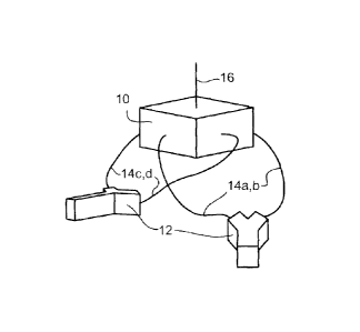
FIG. 2 is a schematic illustration of the overall OMT design in accordance
with the
invention. The OMT uses a turnstile 10 as the principal junction, which
couples
polarization diplexed waveguide 16 and four waveguide paths 14a,b,c,d. The
waveguide
paths 14 as they exit the turnstile 10 are perpendicular to the diplexed
waveguide 16,
paired waveguide paths 14a,b, and 14c,d are oppositely directed, and unpaired
waveguide paths 14a,c, 14a,d, 14b,c, and 14b,d are perpendicular. As such, the
directions of the diplexed waveguide 16 and waveguide paths 14 coordinatize 3
space
with the diplexed waveguide 16 in the positive z direction, waveguide paths
14a,b,c,d
going in +x,-x,-1-y,-y directions, respectively. The turnstile has a matching
feature that
reduces return losses of the polarization diplexed waveguide, as is described
further
herein below.
The paired waveguide paths 14a,b (and likewise with paired waveguide
paths 14c,d) include bends in a manner known in the art of waveguide
construction, such
that the paired waveguide paths rejoin at an E-plane Y junction 12. As
illustrated, the
bending of the paired waveguide paths 14 is entirely schematic, however, it is
necessary
that the electrical lengths of each waveguide path be the same as that of its
paired
waveguide path, in order to provide constructive interference, as will be
appreciated by
those of skill in the art. A wide variety of examples of layouts are possible
to achieve this
result, some of which are described herein below.
The waveguide, turnstile, and Y couplers may be milled from solid blocks or
surface formed by precision molding, stamping or engraving, using such
techniques as
electrical discharge machining, electroforming, etching with lasers or
chemical etchants,
and possibly casting or forging, depending on the tolerances required, the
material used,
and the dimensions of the features. The material may be formed of a plastic
but be
coated with a surface conducive to operation in an OMT. The waveguide paths 14
are
preferably formed by straight path sections of uniform cross-section segmented
by 2 or
more bends that can be characterized as H-plane or E-plane bends (i.e. bends
are only in
planes perpendicular or parallel to the x, y and z coordinates), although this
is not
9
CA 02801948 2012-12-07
WO 2011/153606
PCT/CA2010/000864
essential. In the illustrated embodiments the bends are all 90 or 180 bends,
but this is
not essential. The straightness of the path segments, 90 bends, and
orientation of the
bends in planes perpendicular/parallel to the coordinates, are all preferred
because of the
ease of manufacture, and reproducible quality parameters.
Naturally each component of the OMT design increases reflection losses, and
cross-polarization, and decreases isolation of the OMT, in operation. Some
components
are more sensitive than others. For example, substantially uniform cross-
section, straight
waveguides (square profile is used, although this is not essential) contribute
very little to
the losses. In the designed and produced examples herein, the return losses of
the
components are substantially ordered as follows: Turnstile junction with
matching feature
(-30 dB); E-plane power combiner (--40 dB); bends (--45 dB); and an optional
transformer of the diplexed waveguide (--55 dB).
Each component of this device was simulated and provides return loss across a
38% bandwidth that is believed to be scalable to frequencies up to 500 GHz.
The
techniques for forming can advantageously be CNC machining.
Matching elements
The turnstile junction of the illustrated embodiments includes a matching
feature
that is designed to reduce return losses, and efficiently couple
electromagnetic radiation
from the polarization diplexed waveguide to the waveguide paths, and vice
versa.
While various features are known in the art, and still more may yet be defined
that
have particular advantages for specific applications, Applicant considered 4
matching
features for broadband OMTs: a cubic feature, a cubic feature with 4 pins, a
truncated
pyramid, and a cylindrical feature. Nonetheless Applicant envisages variations
on these
features including: 3 superimposed cylinders, a cone, and the addition of
peripheral
elements (such as the 4 pins) to any of the above features. Typically matching
features
have at least 4 fold symmetry such that each 90 section of the matching
feature
associated with a respective waveguide port, is the same.
FIG. 2 schematically illustrates these 4 matching features. The specific
turnstile
illustrated has a circular polarization diplexed waveguide (diameter 7.42 mm),
and
waveguide paths having a width of 6.33 mm, and a height of 3.25 mm. FIG. 2a
schematically illustrates a cubic matching stub in a turnstile. The cubic stub
has square
lengths 2.97 cm, and a height of 1.27 cm. This type of matching feature has a
return loss
profile (as determined by simulation) over a frequency range of 30-44 GHz that
is less
CA 02801948 2012-12-07
WO 2011/153606
PCT/CA2010/000864
than -24 dB. FIG. 2b has, in addition to the stub, 4 pins, acting as inductive
posts, that
are positioned midway between corners where the waveguide paths meet, and
corners of
the stub. The pins have diameters of 0.3 mm and height of 0.4 mm. The addition
of
these pins decreases the return loss to -24.2 dB and extends the range over
which this
return loss is provided beyond 46 GHz, as determined by simulation.
FIG. 2c schematically illustrates an idealized matching feature used by
Navarrini
et al. adapted to the turnstile dimensions and wavelength band of 30-45 GHz.
The cubic
section has sides 2.667 mm long, and a height of 0.575 mm. The base section
has a
height of 0.84 mm and a profile contour from a 4.56 mm base to the 2.667 mm
top having
a fillet radius of 1.3 mm, on all four sides. By simulation this design is
found to provide a
return loss of -25 dB at least from 30-45 GHz
FIG. 2d schematically illustrates a matching feature currently preferred, at
least for
operation within the 31.3-45 GHz ALMA band 1. The feature includes two
concentric
cylinders: the base cylinder having a diameter of 4.895 mm, and a height of
0.682 mm,
and the top cylinder having a diameter of 2.2 mm, and a height of 1.293 mm.
Over ALMA
band 1, the return losses are less than -30 dB. From 31.8-45 GHz the return
losses are
less than -33 dB, return losses are -35 dB across 82% of the ALMA band 1 (i.e.
from
about 32.7-44.7 GHz) and -40 dB across 71% (i.e. from about 33.9-44.3 GHz),
and about
-42.4 dB or less from about 34.4-44.2 GHz, i.e. over 2/3 of the ALMA band. The
return
losses are minimum in the neighbourhoods of 36 GHz, and 43.5 GHz.
Given the improvement provided by the 4 pins on the cubic stub, where the 4
pins
are arranged substantially midway between the stub and the (projected) limits
of the
polarization diplexed waveguide, it is possible that other stubs may have
return losses
improved by inclusion of these or one or more other elements around the stub.
In accordance with an aspect of the invention, the OMT is formed of at least 3
blocks that are assembled to form the OMT. Two of the blocks have mating
surfaces
defining an interface. The interface defines the turnstile, including at least
the matching
feature and an initial part of the 4 diverging waveguide paths.
By avoiding the quartered-block arrangement of Navarrini et al., which
produces
parts of the matching stub on each of the blocks, alignment and assembly is
greatly
facilitated. Advantageously, the matching feature can often be provided by
machining
without any special bits. While this is advantageous, it will be appreciated
that for OMTs
adapted to other bands, and for applications requiring lower return losses,
for example,
11
CA 02801948 2012-12-07
WO 2011/153606
PCT/CA2010/000864
matching features may alternatively be provided in other ways. The matching
feature
does not need to be machined into the mating surface of the single interface
that defines
the turnstile, but may include elements that are smaller or more delicate than
can be
produced by CNC milling, for example. On a single part, it is possible to
place the
matching feature in a number of ways, including laser ablation or using other
fine
resolution machining techniques.
Each component of this device was simulated and provides return loss across a
38% bandwidth that is believed to be scalable from frequencies as high as 500
GHz.
With more exotic machining or other forming techniques, higher frequency OMTs
can be
produced. The techniques for forming can advantageously be CNC machining,
which
can provide features having dimensions as small as 60 pm with a tolerance of
+1- 5 pm.
While the foregoing examples are advantageous in that they can be milled by
CNC machining, like all of the other parts of the OMT, making for simplified
fabrication, an
advantage of the present design is that all of the matching elements are
provided on one
part, and on one surface thereof, and that unrestricted access is provided to
this surface
when the OMT is in disassembled form. A wide variety of stubs and features in
general
are possible with the variety of deposition techniques available, and the
stubs may be
composed of materials having similar thermal expansion coefficients but
different
permeabilities and permittivities resulting in different effective refractive
indices. These
exhibit different abilities for redirecting electromagnetic radiation of
different
radiofrequencies and modes. Continued research into higher frequency bands are
expected to yield different features that are particularly applicable to
different bands.
E-plane Y junction
Applicant has chosen a design for the E-plane power combiner that has
advantages over Navarrini's design, in terms of compactness and performance.
As will
be seen in FIG. 4(a), Navarrini's E-plane Y junction uses radially curved
arcuate bends
leading the two decoupled ports to a junction region, and employs a 3 section
impedance
transformer between the coupled port and the junction region. FIG. 4(b), in
contrast,
shows a 4 section transformer section, and employs a tight corner (right angle
inside)
bend that is defined by a 3-part miter corner. It will be appreciated that a
different number
of miter parts could alternatively be used, especially a higher number, and
alternatively a
multi-step corner could be used, and may be preferred, depending on the
direction of
machining, the equipment used for machining, and performance requirements.
12
CA 02801948 2012-12-07
WO 2011/153606
PCT/CA2010/000864
Graphs in FIGs. 4(a) and 4(b) show how simulated results in the ALMA band 1
demonstrate a markedly lower return loss for this more compact E-plane Y
junction. The
prior art example by Navarrini had a -30 dB return loss across a 43%
bandwidth.
FIG. 3(b) shows two embodiments of E-plane Y junctions: one with a 3-part
mitre
septum/bend, and one with a 2 step septum/bend. Both use a 4 step impedance
transformer. The 2 step Y junction exhibits a 48.7% bandwidth with a return
loss of -30
dB, a -39.5 dB return loss over a 32% bandwidth, and a -42 dB return loss over
a 25%
bandwidth. The 3-part mitre Y junction exhibits a -40 dB return loss across a
44%
bandwidth and a 49.3% bandwidth at -30 dB. Simulations demonstrate a
substantially
lower return loss for this more compact E-plane Y junction.
It will be noted that this design can advantageously be milled and/or drilled
into a
solid workpiece from 2 directions with respect to the plane of the Y junction
(i.e. the plane
in which the letter Y is formed). When the plane of the Y-junction lies
between two
mating surfaces of adjacent parts, the milling can be provided in the
direction of the H-
field; and where the two mating surfaces sever the Y junction around the
junction region,
such that a septum of the Y junction is defined by a first part and the entire
transformer
section is defined by another, the milling is provided in a direction (k) of
the waveguide if
the blocks are aligned in a stack, and thus access is only provided at two
surfaces.
Alternatively the Y junction oriented parallel to the diplexed waveguide and
offset from the
axis of the diplexed waveguide may be provided on a side of the block defining
the
diplexed waveguide, and/or the matching feature. The Y junction design with
arcuate
bends (FIG. 4(a)) can be milled from only one side (the direction of the H
plane).
Furthermore, the Y junction of FIG. 4(b) permits a more compact arrangement,
which is
generally desirable of OMTs. Given a distance between the junction region and
the
coupled port, a high aspect ratio bit may be required to machine this part,
when it is
produced end-on. As this may contribute to errors in the device, higher
rigidity (specialty)
bits may be required, or the part in which the device is machined may be diced
transversely to the axis of the Y junction. This permits different stages of
the transformer
to be defined at different mating surfaces of the parts, and removes the
requirement to
use longer or higher aspect ratio bits. Furthermore, the sections of the
transformer may
be provided in separate planar parts having through holes. These solutions
increase the
parts count and may add to the requirements for alignment, and present
difficulties with
assembly. Mismatch may also adversely impact on the quality of the OMT (return
loss,
cross-polarization, and isolation). For these reasons, Applicant has chosen to
produce
examples having E-plane Y junctions on mating surfaces of the parts such that
the E-
plane Y junctions are defined by 2 mating surfaces on distinct blocks.
13
CA 02801948 2012-12-07
WO 2011/153606
PCT/CA2010/000864
It will be noted that simulations used to provide the graphs in FIG. 4(b), in
the
case of the 3-part mitre Y junction, took into consideration a rounding of
corners that
result from milling with a carbide end mill, diam. 2 mm, length of cut=9 mm,
where the
milling is performed in the plane of the Y junction. This makes the graph of
the 3-part
mitre Y junction more accurate than that of the 2 step Y junction.
Nonetheless, the 2 step
Y junction graph shows the potential of 2+ step septum/bend Y junctions to be
used with
minor penalty to bandwidth and quality.
Bends
A variety of bends are possible, each offering different advantages in terms
of
return loss, and ease of machining, dependendence on the orientation of the
bend with
respect to the mating surfaces, and whether they are E-field or H-field bends.
In general
there are tight corner bends, in which an inside corner of the bend is a right
angle (i.e.
waveguide segments of the waveguide path meet at a (usually square) edge on
the
inside corner) and arcuate bends, which are not as compact. FIG. 5 includes
six panels,
each having a return loss spectrum and an associated H-plane bend layout. The
graphs
are of return loss s (dB) as a function of normalized frequency, as before.
Similar
results are provided by E-plane bends in terms of return losses. It will be
noted that the
return loss spectra are expressed in relative units, with respect to the
cutoff frequency.
While the instant graphs were produced targeting a 75-115 GHz band, as is well
known in
the art, a design properly scaled to a respective band has substantially
equivalent overall
bandwidth and return loss coefficients in other scales for other bands.
It will be noted from the top right panel that a tight corner bend with a
rounded
outside corner has a uniform return loss of about -20 dB over at least 1.3-
1.95 relative
frequency range, and is relatively flat. A single step tight corner bend or a
single mitered
tight corner bend has an excellent return loss (>-35 dB) from 1.65-1.9
normalized
frequencies, and has -20 dB return loss between 1.35 and 1.95. A 2-miter
corner and a 3
miter corner improve the overall return loss to better than -20 dB and nearly -
40 dB,
respectively. The foregoing bends are preferred for their compactness, and the
ease with
which they can be defined (i.e. using only standard CNC machining, from any of
three
directions) in comparison with arcuate bends. The radial arcuate bend exhibits
a nearly -
25 dB return loss with an inner curvature of 1.5 wavelengths. To improve this
latter
example the radius has to be increased, further detracting from compactness of
the bend.
Square bends (tight corner with square outside edge) are also preferred;
however
these are difficult to produce by drilling and endmilling. Other forming
techniques can be
14
CA 02801948 2016-12-08
used to produce square corners, such as electroforming, as taught, for
example,
by Nesti in a paper entitled "Orthomode Transducer at 43GHz", (Ufficio
lnnovazione
Tecnologica - INAF, 2006-2007,
http://www.arcetri.astro.it/-nesti/pdfs/TecRepOMT43GHz.pdf. the contents of
which are
understood by those of skill in the art.
FIG. 5a schematically illustrates 3 specific H-plane bends that are considered
for
applications in the ALMA band 1: a 3-part miter bend (the center part sweeping
an angle
of 30.8 , and having a width of 5.848 mm and the two symmetric side parts
sweeping
angles of 29.6 ); a 2 step bend and a 3 step bend (both symmetric about the
dashed line,
having dimensions shown). For the ALMA band 1, the waveguide paths may be
rectangular, having dimensions: 6.33 mm by 3.25 mm. The 3-part miter H-plane
bend and
3-step H-plane bend were simulated and have return losses of -45 to -50 dB,
and are
below -60 dB over at least 2/3rds of a 40% bandwidth.
As the bends are also preferably formed by CNC machining, there will be some
rounded corners (on the axis of the bit). Simulations show that the 3 step H-
plane bend
(with 1 mm diameter rounded corners) where the milling is performed in a
direction of the
E-field), exhibits a return loss of about -48 dB across a 40% bandwidth. The
return loss is
below -60 dB over 4/51hs of the 40% bandwidth. A 3 step H-plane bend (with
unrounded
corners), exhibits a return loss of -45 dB across a 40% bandwidth, and a
return loss below
60 dB over 62% of that bandwidth.
FIG. 5b schematically illustrates 3 specific E-plane bends that are considered
for
applications in the ALMA band 1: a 3-part miter bend (the center part sweeping
an angle
of 15.104 , and having a width of 2.8694 mm and the two symmetric side parts
sweeping
angles of 37.448 ); a 2 step bend; and a 3 step bend (both symmetric about the
dashed
line, having dimensions shown). The 2 step E-plane bend (with 1 mm diameter
rounded
corners) where the milling is performed parallel to the E-field of one end and
in the
waveguide (k) direction at the other end, has a simulated return loss of -41
dB over a 40%
bandwidth, over 70% of which the return loss is below -45 dB. In comparison a
3 step E-
plane bend with the same rounding has a simulated return loss of -44 dB over
the 40%
bandwidth, and is -50 dB over nearly 4/5ths of that bandwidth, and over about
half the
bandwidth, is -54 dB.
A study of 2 step E-plane bends was performed to determine an importance of
the
diameter of the milling bit and the consequent rounding of the edges. It was
noted that -
32, -35, -38, -42, and -46 dB losses are provided respectively by bends with
3, 2.4, 2, 1.5,
CA 02801948 2012-12-07
WO 2011/153606
PCT/CA2010/000864
and 1 mm rounding. At 0.5 and 0 mm roundings, -54 dB return loss is provided.
Similar
results are expected for other bends and straight waveguide sections.
Applicant has
chosen the 1 mm rounding for examples described below.
Polarization diplexed waveguide
As is well known in the art, a matching is required between a width of the
waveguide paths, and that of the diplexed waveguide and the phase constant of
the
signal (beta), in order for the turnstile to operate efficiently. Typically
the diplexed
waveguide is 2 fold symmetric (e.g. square or circular), and the waveguide
paths are
rectangular having a width (determining a cut-off frequency of the EM
spectrum) and a
height that is some fraction (1/2, 1/3, etc.) of the width. A transformer is
typically required
depending on the source and drain waveguides coupled to the OMT. To illustrate
how
this may be performed, a transition between a 7.9 mm to a 7.419 mm diameter
(circular)
polarization diplexed waveguide is used as an impedance transformer the
prototype
embodiment. It will be appreciated that different impedance matching
transitions may be
incorporated into the OMT, at the three OMT ports for example, or these may be
provided
outside of the OMT at adapters.
Applicant considered 3 transformer arrangements: a 3-stage Chebytchev
transformer (d=7.419 mm I d=7544 mm, h=2.496 mm 1 d=7748 mm, h=2.458 mm 1
d=7.9 mm), a 3-stage polynomial transformer (d=7.419 mm 1 d=7527 mm, h=2.5 mm
1
d=7768 mm, h=2.455 mm 1 d=7.9 mm), and a 2 stage quarter wave transformer
(d=7.419 mm 1 d=7644 mm, h=2.477 mm 1 d=7.9 mm). The return loss attributed to
the
quarter wave transformer element is -39 dB over a 42% bandwidth, and -50 dB
over a
25% bandwidth. The polynomial transformer had a simulated return loss of -44
dB over a
42% bandwidth, with -50 dB return loss over 90% of that bandwidth and -60 dB
over at
least 60% thereof. The Chebytchev transformer simulation showed the best
return loss,
being -48 dB over the 42% bandwidth -55 dB over 92% of the bandwidth, and
about -57
dB over 88% thereof.
Design layouts
FIGs. 6a-g schematically illustrate 7 design layouts combining the above
described features. FIG. 6a shows a first design layout of the invention,
which is currently
preferred because it is amenable to construction with only 3 blocks. This
first design was
constructed and tested, and the results are described below. This embodiment
was
simulated, and FIG. 6a shows a scalar E-field diagram of the layout, in two
images. A
simpler model of this design is presented in FIG. 7a. The 3 blocks are stacked
one on
16
CA 02801948 2012-12-07
WO 2011/153606
PCT/CA2010/000864
top of the other. A first interface between the bottom and intermediate blocks
provides
the surface for the turnstile matching feature, as well as initial segments of
the waveguide
paths, which in both cases, consist of a straight segment, followed by an H-
plane bend,
followed by another straight segment, followed by the start of an E-plane bend
that takes
the waveguide path out of the plane of the turnstile. Through-holes in the
intermediate
block communicate between the E-plane bends and H-plane bends, which are
aligned
with respective segments that lead to respective branches of the Y junctions.
Thus each
waveguide path follows a bends sequence HEH. Both Y junctions, as well as the
segments leading to their respective branches are defined at the interface
between the
intermediate and top blocks. To this degree, both arms (an arm consists of one
pair of
the waveguide paths that were initially oppositely directed, that extend from
the turnstile
to a common Y junction) of the OMT design are the same. However, it will be
noted that
a smaller arm is symmetric (the lengths of the segments of the waveguide paths
are both
abca), whereas the lengths of those of the longer arm are abcd and dbca,
respectively
(ignoring differences in the dimensions of the turnstile and Y junctions). The
assymmetry
improves compactness of the OMT. The longer arm could be longer, and
symmetric.
An advantage of having the Y junctions defined at the plane above the
turnstyle,
as it could equally be made below the plane of the turnstile, is that the
interface between
the top and intermediate blocks can be used to machine the diplexed waveguide
transformer. Where such a transformer is not desired, the second interface may
be
below the first, such that the alignment of the diplexed waveguide is
controlled by the first
interface independently of the alignment of the waveguide paths at the second
interface.
Alignment of these three blocks in a stack is easier than most other
arrangements. This
layout is particularly preferred for miniaturization, which is important for
higher frequency
OMT designs.
FIG. 6b schematically illustrates an alternative embodiment of a design in
accordance with the invention. The design has a larger arm that is identical
to the small
arm of the design of FIG. 6a, and is not described again. The smaller arm of
FIG. 6b is
substantially optimally compact, consisting of two 90 E-plane bends between
three
segments. While it would be intuitive to use an H-plane Y junction to make the
larger arm
of the same effective size as the smaller arm, to produce a more compact
design, H-
plane bends are significantly lower quality bends, and are not chosen for this
reason.
The EE bend sequence must be defined by the plane of the turnstile and a
second plane
parallel to and below that of the turnstile. The longer arm extends to a plane
above the
turnstile, as it did in FIG. 6a. Accordingly, this design may be provided with
a four block
17
CA 02801948 2012-12-07
WO 2011/153606
PCT/CA2010/000864
stack: 1) a bottom block through which the shorter arm Y junction extends,
having a lower
interface with a second block where the waveguide path segments connecting the
waveguide paths of the shorter arm to the Y junction are defined; 2) the
second block
through which the waveguide paths of the shorter arm pass, defining a mid
interface with
a third block at which the turnstile matching feature and initial segments of
the waveguide
paths are defined, wherein lies the plane of the turnstile; 3) the third block
having through
holes for the longer arm, and forming a higher interface with a top block at
which the Y
junction of the longer arm is defined, and through which the transformer
section of the
diplexed waveguide is bored; and 4 the top block having the diplexed waveguide
throughbore.
As noted in relation to FIG. 6a, it is convenient to provide the longer arm
above
the plane of the turnstile to provide access to the diplexed waveguide for
forming the
transformer, which is desired in many applications. However, if (for example)
coupling to
a variety of waveguides is desired, the transformer may be provided outside of
the OMT.
If so, the E-plane bends in the longer arm may be oriented downwards, instead
of
upwards, and the Y junction may be defined at the same block interface as the
segments
leading to the Y junction in the short arm. This would reduce the number of
blocks to 3,
obviating the higher interface between the second and top blocks. While the
number of
blocks increases the number of steps in assembly and alignment, the ability to
independently align respective waveguide paths of the OMT may be preferred in
some
embodiments.
Moreover, depending on the tolerances and the requirements of the Y junction,
it
may be difficult or expensive to mill the shorter arm Y junction depth-wise
into the bottom
block. This can be avoided by adding additional blocks, so that they are
stacked
horizontally, or by splitting the bottom block in a direction perpendicular to
the lower
interface.
It will be noted that when defining an interface between two blocks (according
to
any embodiment), it is generally preferable to mill only one side of the
interface, as this
generally reduces a sensitivity of alignment, and reduces the amount of
milling. At the
mid interface, the milling direction is chosen by the position of the matching
feature, when
this is machined. If the matching feature is not milled into the piece, it may
be precision
aligned, for example after the OMT is assembled, at an optimal position, in
which case
the milling can be performed on either surface of the mid interface. But in
any case,
where the mid interface has bends upwards and downwards, shoulders for one of
the
bends would need to be milled in the otherwise flat surface. Solutions to this
include:
18
CA 02801948 2012-12-07
WO 2011/153606
PCT/CA2010/000864
adding protruding elements on the flat surface aligned with the throughholes
(for example
by placing the features after the adjacent block with through holes are
assembled); milling
the shoulders out of the otherwise flat surface; and selecting an interface
line
intermediate the top and bottom walls of the waveguides. The last option
requires milling
in both surfaces, but generally less milling is required than in the second
example.
Additionally a seam is provided in the waveguides, which may be preferred.
FIG. 6c shows an alternative OMT design having two symmetric arms: a shorter
arm corresponding to the EE bend sequence of FIG. 6b; and a longer arm that
consists of
two H-plane bends leading to the Y junction, which begins in the plane of the
turnstile.
This OMT design is amenable to three block formation, if longitudinal milling
of the Y
junctions is possible. This is not easy with standard CNC machining.
Accordingly, a
fourth block may be required. The four block configuration includes a stack
of: a top
block defining the diplexed waveguide; a middle block, through which part of
the Y
junction on the longer arm, and the through holes of the short arm, are
defined; and a
bottom block assembly that is split perpendicularly to the interfaces of the
stack to pass
through both Y junctions. A top interface between the top block and middle
block defines
the matching feature, and initial segments of the waveguide paths, as well as
the top of
the Y junction of the longer arm. A mid interface between the middle block and
block
assembly defines the top of the Y junction of the shorter arm, and parts of
the waveguide
paths leading thereto. A split interface of the block assembly defines the
bottoms of the Y
junctions. Given the aspect ratio of full height waveguides, there will
generally be a
requirement for milling on both sides of this split. An advantage of the
embodiment of
FIG. 6c is that both polarized outputs of the OMT are parallel.
FIG. 6d is an alternative OMT design including a long arm corresponding to the
longer arm of FIG. 6c and a short arm corresponding to the shorter arm of FIG.
6a. This
can be embodied in a three block stack having interfaces for the short arm Y
junction
(and transformer), and turnstile plane, and the bottom block may be split to
accommodate
CNC machining of the long arm Y junction. Alternatively, the long arm Y
junction could
be machined at an interface between a bottom block and a side block.
Advantageously,
by milling the bottom block on two adjacent sides, the side block would have
no milling
and no alignment constraints. This is a possible alternative block arrangement
for all Y-
couplers that extend in the direction of the diplexed waveguide, at a
periphery of the
OMT, in the plane of the turnstile.
FIG. 6e is an alternative OMT design including the HH bend sequence short arm,
and a long arm having one waveguide path detouring around the short arm
waveguide
19
CA 02801948 2012-12-07
WO 2011/153606
PCT/CA2010/000864
path with an over-pass. An over-pass can be included in other designs. The
long arm
consists of two waveguide paths: an HEEEEH bend sequence path, and an HH bend
sequence path. These paths are non-symmetric. This embodiment can be produced
with a stack of 3 (top, mid, bottom) horizontal blocks, with an upper
interface between the
top and mid blocks defining the over-pass of the HEEEH bend sequence path, and
a
lower interface between the mid and bottom blocks defining the turnstile
plane. The Y
junctions may be machined longitudinally into the bottom block, or on two
adjacent sides
of the bottom block to be covered by flat slabs, such that the bottom block is
milled on
three mutually adjacent sides, for example. Alternatively the lower block
containing the Y
junctions may be split.
FIG. 6f is an alternative OMT design showing a symmetric, HH bend sequence
arm (although a non-symmetric arm could alternatively be chosen to make the
OMT more
compact, see: FIG. 6a, longer arm), and a symmetric arm, each waveguide path
having
HHEE bend sequences. This design is amenable to construction with a three
block stack
(top, mid, bottom), where an upper interface (top/mid) defines the "HHEE" arm
Y junction
and leads, the mid block defines segments of the HHEE and the lower interface
(mid/bottom) defines the rest. The lower block may define the "HH" arm Y
junction on a
side of the block, requiring another slab, and the top block may be split to
define the
HHEE arm Y junction. Alternatively, this layout may be provided by a top block
assembly
and a bottom block (with or without the side slab), the top block assembly
having a split in
the plane of the HHEE arm Y junction. This split may essentially consist of a
side slab, if
the top block is milled on two adjacent sides. This design therefore permits
construction
with two blocks, each milled on 2 adjacent sides, with 2 additional slabs.
While milling on
two sides increases a complexity of the milling operation, it simplifies
alignment
considerably, and is considered preferable for some applications.
With the general design of FIG. 6f, a selection of (non-minimal) lengths of
the
waveguide paths of the HH arm and a height of the over-pass can be made to
provide
equal path lengths for all four waveguide paths. Alternatively, by reducing
the path
lengths in the HH arm, the HH arm Y junction may be shifted to lie in a plane
with the Y
junction of the HHEE arm, offering other options for manufacturing.
Finally, as noted above, the HHEE arm Y junction may be directed in the same
direction as the HH arm Y junction, resulting in the two slabs (possibly)
meeting along an
edge, which could be replaced by an elbow-shaped piece.
CA 02801948 2012-12-07
WO 2011/153606
PCT/CA2010/000864
FIG. 6g shows an alternative layout for an OMT, in which each waveguide path
consisting of HHEE bend sequences, one of which providing an over-pass. Again
path
lengths may be chosen so that both arms have equal electrical lengths. Y
junctions are
both oriented up. The design is amenable to construction using two blocks,
with a top
block being milled on three mutually adjacent sides, along with two side parts
and a
bottom block. One of the side parts includes a part of a waveguide path that
effectively
provides an overpass to the short arm. The bottom has the matching feature,
and may
have no other feature. A side wall of the top block is milled on sides for the
optical paths
leading to the Y junctions. The featureless slabs may be of any material,
thickness, or
form to provide single walls of these waveguide paths.
While the foregoing examples used relatively few parts, up to 6 blocks can be
precisely oriented, especially when the position of one block at one interface
is dependent
on 2 or fewer other blocks, and the mismatch of the blocks are not highest in
the regions
of highest sensitivity (such as the matching feature of the turnstile plane).
Other
embodiments are equally possible, and the foregoing are merely intended as
illustrative.
Other combinations of arms (HH, EE, HEH, HHEE, symmetric and non-symmetric,
etc.)
of the different examples are equally contemplated. It will be noted that
replacing a HEH
bend sequence path with an EHE bend sequence path is substantially equivalent
in terms
of orientation of the waveguide, and other similar substitutions are
immediately obvious to
those of skill in the art, and do not constitute a substantial variant of the
layout.
It will be noted that while all of the foregoing examples use only straight
waveguide segments, 900 bends, waveguide segments having full height, and
that,
except for the power transformer in the diplexed waveguide, the waveguide
segments are
all of constant dimension, one of skill in the art may vary from these
conventional
preferences, and these are not intended to be limiting, as consequences to
varying these
parameters can be determined using known software.
Example
To manufacture an OMT in the 30-45 GHz band, we used a conventional CNC
machining with standard carbide end mills (no exotic diameters or lengths of
cut). A block
of aluminum was diced and surface formed by milling, and throughbores were
made by
drilling. The waveguide paths were rectangular, having dimensions (WR22: 6.33
x
3.25 mm2), but this design could be used from WR-650 (1.12-1.7 GHz, 16.51 x
8.255
cm2) to WR-3.7 (200-270 GHz, 0.94 x 0.47 mm2) and beyond for both narrow and
broadband OMTs.
21
CA 02801948 2012-12-07
WO 2011/153606
PCT/CA2010/000864
FIG. 7a is a photograph of two of the OMTs produced, one in assembled, and the
other in disassembled form. The turnstile plane is shown on the middle block
at the far
right, of the disassembled OMT, revealing the matching feature and initial
segments of
the waveguide paths, and H plane bends. Various holes were used for alignment
of the
OMT blocks. The assembly is quick and the precision of alignment is excellent.
The
machining tolerances were between +/- 20 pm (for bends and waveguide paths
outside of
the plane of the turnstile) and +/- 10 pm (at the plane of the turnstile). A
surface
roughness better than 1.6 pm for the mating surfaces was demanded. A 10 pm
parallelism, perpendicularism and surface flatness were required.
An Anritsu vector network analyzer (VNA) is used to measure s-parameters of
the
OMT. A schematic of the cross-polarization test setup is shown in FIGs. 7b,c.
Maury
Microwave Corporation J237B6 waveguide-to-coaxial adapters were used to join
the
coaxial test cables to WR22 waveguides. A circular-to-rectangular waveguide
adapter
was used on the circular input guide. The rectangular waveguide for the
orthogonal
polarization was terminated with a Quinstar Tech. Inc. fixed termination.
Polarization 1 or Polarization 2 was excited by rotating the input transition
by 90
at the circular waveguide flange. The Short, Short, Load, Through (SSLT)
calibration
procedure, well known in the art, was used to remove systematic instrumental
effects and
to calibrate out the response of the coaxial cables and coax-waveguide
transitions in the
test circuit.
FIGs. 8a,b,c,d are graphs showing S-parameter measurements taken on four
OMT devices. It is noted that insertion loss is measured using both ports of
the VNA in
the configuration presented in FIG. 7c. The loss of the circular-to-RWG
adapter was
calibrated by measuring the loss of two such transitions back-to-back. The
insertion loss
(FIGs. 8a,c) was between -0.11 and -0.25 dB through port 2, and between -0.12
and -
0.28 dB through port 3 across the ALMA band 1 and beyond, for all four OMTs.
The
insertion loss is substantially flat, and reproducible across a broad 30-45
GHz (37%)
bandwidth. The cross-polarization was less than -42 dB for polarization 1, and
-40 dB for
polarization 2 over the full 42% bandwidth shown.
FIGs. 9a,b,c graph the return loss of each of the ports of the four OMTs. In
each
case the return loss is < - -25 dB, is relatively constant across the
bandwidth, and highly
repeatable. The polarization diplexed port (Si) shows a return loss < -27 dB.
22
CA 02801948 2012-12-07
WO 2011/153606
PCT/CA2010/000864
The OMT isolation was obtained by measuring the transmissions between the
OMT (uniplex) ports with its circular waveguide input port open to free space.
An
absorber was placed in front of the polarization diplexed waveguide. This
gives an upper
limit of the isolation of the device which should be measured. The isolation
was found to
be less than -60 dB across the ALMA band 1, and beyond.
Broadband applications (up to 44%) with return losses less than -27 dB,
isolation
better than -60 dB and cross-polarization better than -40 dB are shown.
Narrowband
applications (up to 22%) with return losses better than -30 dB, isolation
better than -60 dB
and cross-polarization better than -45 dB have been shown.
Other advantages that are inherent to the structure are obvious to one skilled
in
the art. The embodiments are described herein illustratively and are not meant
to limit
the scope of the invention as claimed. Variations of the foregoing embodiments
will be
evident to a person of ordinary skill and are intended by the inventor to be
encompassed
by the following claims.
23