Note: Descriptions are shown in the official language in which they were submitted.
CA 02802136 2013-01-10
42867-CA-PAT
COMMUNICATIONS DEVICE AND METHOD FOR HAVING INTEGRATED NFC
ANTENNA AND TOUCH SCREEN DISPLAY
Technical Field
[0001] This application relates to the field of
communications, and more particularly, to mobile wireless
communications devices and related methods that use Near Field
Communications (NFC).
Background
[0002] Mobile communication systems continue to grow in
popularity and have become an integral part of both personal and
business communications. Various mobile devices now incorporate
Personal Digital Assistant (PDA) features such as calendars,
address books, task lists, calculators, memo and writing
programs, media players, games, etc. These multi-function
devices usually allow users to send and receive electronic mail
(email) messages wirelessly and access the internet via a
cellular network and/or a wireless local area network (WLAN),
for example.
[0003] Some mobile devices incorporate contactless card
technology and/or Near Field Communication chips. Near Field
Communications technology is commonly used for contactless
short-range communications based on radio frequency
identification (RFID) standards, using magnetic field induction
to enable communication between electronic devices, including
mobile wireless communications devices. These short-range
CA 02802136 2013-01-10
42867-EP-EPA (85353-EP)
communications include payment and ticketing, electronic keys,
identification, device set-up service and similar information
sharing. This short-range high frequency wireless
communications technology exchanges data between devices over a
short distance, such as only a few centimeters.
[0004] As Near Field Communication (NFC) technology becomes
more commonplace, it is often used with portable wireless
communications devices in association with other short-range
wireless communications such as a wireless Bluetooth connection.
For example, an NFC connection is often used to establish a
wireless Bluetooth connection in which data for establishing the
Bluetooth connection is communicated. It is desirable also to
accommodate NFC components such as the antenna in confined
spaces of the device.
Brief Description of the Drawings
[0005] Other objects, features and advantages of the present
invention will become apparent from the detailed description of
the invention which follows, when considered in light of the
accompanying drawings in which:
[0006] FIG. 1 is a high-level schematic circuit block diagram
of an example embodiment of a mobile wireless communications
device that uses a touch screen display and NFC antenna
integrated therewith in accordance with a non-limiting
embodiment.
[0007] FIG. 2 is a plan view of the touch sensor pattern that
includes the NFC antenna integrated with the touch screen
2
CA 02802136 2013-01-10
42867-EP-EPA (85353-EP)
display formed by the touch sensor pattern in accordance with a
non-limiting example.
[0008] FIG. 3 is a high-level block diagram showing basic
components of a portable wireless communications device that can
incorporate the functionality of the communications device that
includes the touch screen display and NFC antenna integrated
therewith in accordance with a non-limiting example.
Detailed Description
[0009] Different embodiments will now be described more fully
hereinafter with reference to the accompanying drawings, in
which various embodiments are shown. Many different forms can
be set forth and described embodiments should not be construed
as limited to the embodiments set forth herein. Rather, these
embodiments are provided so that this disclosure will be
thorough and complete, and will fully convey the scope to those
skilled in the art. Like numbers refer to like elements
throughout.
[0010] A communications device includes a housing and a
wireless transceiver and processor carried by the housing and
operative with each other. A Near Field Communications (NFC)
circuit is carried by the housing and coupled to the processor.
A touch screen display is connected to the processor. An NFC
antenna is integrated with the touch screen display and coupled
to the NFC circuit.
[0011] In one example, the touch screen display includes a
touch sensor pattern and the NFC antenna is integrated within
the touch sensor pattern, which could be formed as alternating
3
CA 02802136 2013-01-10
42867-EP-EPA (85353-EP)
transmit and receive capacitive sensor lines. The touch sensor
pattern could also be formed as a plurality of floating
capacitive sensor islands. In another example, the touch screen
display is formed as an elongate input touch pad formed as a
layer of transparent conductive material such as indium tin
oxide (ITO) touch pattern. The NFC antenna is etched within the
ITO touch pattern in an example.
[0012] In another example, the processor is configured to
display on the touch screen display a user interface. The
housing in another example is configured as a handheld portable
wireless communications device.
[0013] A method of making a communications device is also
disclosed.
[0014] In accordance with non-limiting examples, the NFC
antenna is embedded into the touch screen display that operates
as a touch sensor and reduces the cost and thickness of the
overall product. In one example, the NFC antenna is etched into
the touch sensor pattern such as the indium tin oxide (ITO)
touch pattern, thus becoming a part of the touch screen display
and eliminating the requirement of having an extra layer of
antenna.
[0015] Handheld electronic devices may have a number of
different configurations. Examples of such devices include
personal data assistants ("PDAs"), handheld computers, two-way
pagers, cellular telephones, and the like. Many handheld
electronic devices also feature wireless communication
capability, although many other handheld electronic devices are
4
CA 02802136 2013-01-10
42867-EP-EPA (85353-EP)
stand-alone devices that are functional without communication
with other devices.
[0016] Handheld electronic devices are generally intended to
be portable, and thus, are typically a relatively compact
configuration in which keys and other input structures often
perform multiple functions under certain circumstances or may
otherwise have multiple aspects or features assigned thereto.
[0017] In addition to using keys on a keypad, handheld
electronic devices may also use a touch screen. A touch screen
is typically a display screen overlay which provides the ability
to display and receive information on the same display screen.
The effect of the overlay is to allow a display screen to be
used as an input device, removing the keys on the keypad as the
primary input device for interacting with the display screen's
content. Display screens with integrated touch screens can make
computers and handheld electronic devices more useable. A touch
screen or touch screen system typically includes a touch sensor,
a controller or processor, and accompanying software. The
controller communicates user selections to the processor of the
electronic device in which the touch screen is used.
[0018] The LCD touch screen displays have an arrangement of
touch sensors. In typical LCD touch screen displays, in order to
provide a number of input pads in an X/Y matrix arrangement, the
touch sensor can use two stacked indium tin oxide ("ITO")
polyethylene terephthalate ("PET") polyester film layers. The
first ITO PET film layer may include a number of rows of input
pads (X inputs), the input pads in each row being connected in
series. The second ITO PET film layer may include a number of
= CA 02802136 2013-01-10
42867-EP-EPA (85353-EP)
columns of input pads (Y inputs), the input pads in each column
= being connected in series. These alternating rows and columns
can operate as receive and transmit in some examples.
[0019] Referring now to FIG. 1, a mobile wireless
communications device 20 according to the present disclosure is
now described. The mobile wireless communications device 20
illustratively includes a housing 47 and a touch screen display
48 carried by the front of the housing and typically extending
over the front in a substantially rectangular configuration. A
wireless transceiver 46 is carried by the housing, and a
processor 45 is carried by the housing and coupled to the
wireless transceiver (e.g., cellular transceiver). The mobile
wireless communications device 20 illustratively includes an NFC
IC 21 carried by the housing 47 and coupled to the processor 45,
an NFC antenna 22 carried by the housing, and in one example, an
optional coupling circuit 23 between the NFC IC and the NFC
antenna. The coupling circuit is not required but allows
greater signal control in conjunction with the process.
[0020] The NFC IC 21 could include a plurality of terminals
including a reference voltage terminal (e.g., ground voltage
terminal), an antenna terminal, a receive terminal, and first
and second AC charge terminals. The NFC IC 21 may be configured
to cooperate with the processor 45 to operate in an IC card
emulation mode (NFC device appears to an external reader as a
traditional contactless smart card), a reader/writer mode (NFC
device reads NFC tags), and a peer-to-peer mode (two NFC devices
exchanging data).
6
CA 02802136 2013-01-10
42867-EP-EPA (85353-EP)
[0021] In one example, the optional coupling circuit 23 could
be formed as a capacitive network comprising a plurality of
capacitors coupled in series with each other and in parallel
with the NFC antenna 22 and a transmit branch and a receive
branch. In another example, the coupling circuit could include
first and second tuning branches and be reduced to a single
tuning branch. The housing 47 can be formed as a rigid case for
housing the various components of the communications device.
The touch screen display 48 is typically mounted at the housing
to form a front face of the rigid case. The case preferably
frames the touch screen display and exposes it for user-
interaction.
[0022] It should be understood that the touch screen display
could use mutual capacitance having two distinct layers of
material as described above in which one houses the driving
lines that carry current and the other houses sensing lines that
detect the current at nodes. It could also use self-capacitance
that has one layer of individual electrodes that are connected
with capacitance-sensing circuitry. Both approaches send the
touch data as electrical impulses. It is possible for the
processor based on the touch data to determine the features of
each touch such as the size, shape and location of an effected
area on the screen. It is possible for the processor to arrange
the touches with similar features into groups and calculate
various starting points and use gesture-interpretation.
[0023] The touch screen display 48 is formed in one example
as a capacitive touch screen display. An example of a
description of a touch screen display is described in commonly
7
CA 02802136 2015-01-29
42867 - CA - PAT
assigned U.S. Patent Publication No. 2010/0088654. In one
example embodiment, the capacitive touch screen display can
= include a display device and a touch-sensitive overlay that is a
capacitive touch-sensitive overlay. It will be appreciated that
the capacitive touch-sensitive overlay may include a number of
layers in a stack and is fixed to the display device via a
suitable optically clear adhesive. The layers can include, for
example a substrate fixed to the display device (e.g., LCD
display) by a suitable adhesive, a ground shield layer, a
barrier layer, a pair of capacitive touch sensor layers
separated by a substrate or other barrier layer, and a cover
layer fixed to the second capacitive touch sensor layer by a
suitable adhesive. The capacitive touch sensor layers can be any
suitable material such as patterned indium tin oxide (ITO).
[0024] Each of the touch sensor layers could include an
electrode layer each having a number of spaced apart transparent
electrodes. The electrodes may be a patterned vapour-deposited
ITO layer or ITO elements. The electrodes may be, for example,
arranged in an array of spaced apart rows and columns. The touch
sensor layers/electrode layers are each associated with a
coordinate (e.g., x or y) in a coordinate system used to map
locations on the touch screen display 48, for example, in
Cartesian coordinates (e.g., x and y-axis coordinates). The
intersection of the rows and columns of the electrodes may
represent pixel elements defined in terms of an (x, y) location
value which can form the basis for the coordinate system. Each
8
= CA 02802136 2013-01-10
42867-EP-EPA (85353-EP)
of the touch sensor layers can provide a signal to the processor
45 or a separate controller, which represents respective x and y
coordinates of the touch screen display 48. For example, x
locations can be provided by a signal generated by one of the
touch sensor layers and y locations can be provided by a signal
generated by the other of the touch sensor layers.
[0025] The electrodes in the touch sensor layers/electrode
layers respond to changes in the electric field caused by
conductive objects in the proximity of the electrodes. When a
conductive object is near or contacts the touch-sensitive
overlay, the object draws away some of the charge of the
electrodes and reduces its capacitance. The controller receives
signals from the touch sensor layers of the touch-sensitive
overlay, detects touch events by determining changes in
capacitance which exceed a predetermined threshold, and
determines the centroid of a contact area defined by electrodes
having a change in capacitance which exceeds the predetermined
threshold, typically in x, y (Cartesian) coordinates.
[0026] The processor 48 determines the centroid of the
contact area of the device as the location of the touch event
detected by the touch screen display. Depending on the touch-
sensitive overlay and/or configuration of the touch screen
display, the change in capacitance which results from the
presence of a conductive object near the touch-sensitive overlay
but not contact the touch-sensitive overlay, may exceed the
predetermined threshold in which case the corresponding
electrode would be included in the contact area. The detection
of the presence of a conductive object such as a user's finger
9
CA 02802136 2013-01-10
42867-EP-EPA (85353-EP)
or a conductive stylus is sometimes referred to as finger
= presence/stylus presence.
[0027] It will be appreciated that other attributes of a
touch event on the touch screen display can be determined. For
example, the size and the shape (or profile) of the touch event
on the touch screen display can be determined in addition to the
location based on the signals received at the controller or
processor from the touch sensor layers. For example, the touch
screen display may be used to create a pixel image of the
contact area created by a touch event. The pixel image is
defined by the pixel elements represented by the intersection of
electrodes in the touch sensor layers/electrode layers. The
pixel image may be used, for example, to determine a shape or
profile of the contact area.
[0028] The centroid of the contact area can be calculated by
the processor based on raw location and magnitude (e.g.,
capacitance) data obtained from the contact area. The centroid
is defined in Cartesian coordinates by the value (Xc, Yc)= The
centroid of the contact area is the weighted averaged of the
pixels in the contact area and represents the central coordinate
of the contact area. By way of example, the centroid may be
found using the following equations:
= CA 02802136 2013-01-10
42867-EP-EPA (85353-EP)
11.4
*
)(e.
* yi
Yi=1
c ¨ ¨
zi
i=1
where X, represents the x-coordinate of the centroid of the
contact area, Y, represents the y-coordinate of the centroid of
the contact area, x represents the x-coordinate of each pixel in
the contact area, y represents the y-coordinate of each pixel in
the contact area, Z represents the magnitude (capacitance value
or resistance) at each pixel in the contact area, the index i
represents the electrodes in the contact area and n represents
the number of electrodes in the contact area. Other methods of
calculating the centroid will be understood to persons skilled
in the art.
[0029] In this way, an interrupt signal which indicates a
touch event has been detected, the centroid of the contact area,
as well as raw data regarding the location and magnitude of the
activated electrodes in the contact area are passed to the
11
CA 02802136 2013-01-10
42867-EP-EPA (85353-EP)
processor. However, in other embodiments only an interrupt
signal which indicates a touch event has been detected and the
centroid of the contact area are passed to the processor. In
embodiments where the raw data is passed to the processor, the
detection of a touch event (i.e., the application of an external
force to the touch-sensitive overlay) and/or the determination
of the centroid of the contact area may be performed by the
processor of the device rather than the controller of the touch
screen display.
[0030] FIG. 2 shows the portion of the display 48 that
includes a touch sensor pattern such as generally described
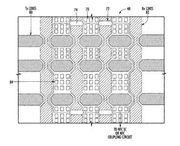
above and illustrated generally at 70 and shows the NFC antenna
72 integrated within the touch sensor pattern. The NFC antenna
72 can include various loop elements 74. The touch sensor
pattern includes alternating transmit and receive lines
indicated generally at 80 and 82. Floating capacitive sensor
islands 84 are also formed. This touch screen display can be
formed as an elongate input touch pad formed over the entire
front housing and formed as a layer of transparent conductive
material such as an indium tin oxide (ITO) touch pattern as
described above. The NFC antenna 72 is etched within the ITO
touch pattern in one example. The loop element 74 can be
positioned over receive lines 82 as illustrated. The NFC
antenna is etched in a substantially rectangular pattern as
illustrated.
[0031] A non-limiting example of various functional
components that can be used in the exemplary mobile wireless
communications device 20 is further described in the example
12
CA 02802136 2013-01-10
42867-EP-EPA (85353-EP)
below with reference to FIG. 3. New reference numerals are
= used. Device 100 is an example embodiment of the device 20.
The device 100 illustratively includes a housing 120, an input
140 and an output device 160. The input 140 could be circuitry
connected to a touch sensitive input such as a display and/or a
separate input, including a keyboard. The output device 160
shown is a display, which comprises a full graphic LCD and is
touch sensitive as an input device in the example described
above. Other types of output devices may alternatively be used.
A processing device 180 is contained within the housing 120 and
is coupled between the input 140 and the display 160. This
device 180 is typically a microprocessor chip contained on a
circuit board in the housing 120. When the display is a touch-
activated display as described above, any keypad is not
necessary. The processing device 180 controls the operation of
the display 160, as well as the overall operation of the mobile
device 100, in response to input by the user.
[0032] The housing 120 may be elongated vertically, or may
take on other sizes and shapes (including clamshell housing
structures). If a keypad is used in addition to a touch screen
display, the keypad may include a mode selection key, or the
device may include other hardware or software for switching
between text entry and telephony entry.
[0033] In addition to the processing device 180, other parts
of the mobile device 100 are shown schematically in FIG. 1.
These include a communications subsystem 101; a short-range
communications subsystem 102; the input 140 and the display 160,
along with other input/output devices 106, 108, 110 and 112; as
13
CA 02802136 2013-01-10
42867-EP-EPA (85353-EP)
well as memory devices 116, 118 and various other device
.
subsystems 121. The mobile device 100 is in this example a two-
way RF communications device having voice and data
communications capabilities using RF circuitry. In addition,
the mobile device 100 has the capability to communicate with
other computer systems via the Internet. The short-range
communications subsystem 102 includes a Bluetooth (BT)
communications module for establishing a Bluetooth wireless
connection and other communications modules such as an infrared
module or device, WiFi circuit and module, and associated
components and circuits as part of RF circuitry.
[0034] Operating system software executed by the processing
device 180 may be stored in a persistent store, such as the
flash memory 116, or may be stored in other types of memory
devices, such as a read only memory (ROM) or similar storage
element. In addition, system software, specific device
applications, or parts thereof, may be temporarily loaded into a
volatile store, such as the random access memory (RAM) 118.
Communications signals received by the mobile device may also be
stored in the RAM 118.
[0035] The processing device 180, in addition to its
operating system functions, enables execution of software
applications 130a-130n on the device 100. A predetermined set
of applications that control basic device operations, such as
data and voice communications 130a and 130b, may be installed on
the device 100 during manufacture. A Near Field Communications
module 130C may also installed as illustrated.
14
CA 02802136 2013-01-10
42867-EP-EPA (85353-EP)
[0036] The NFC communications module 130c as a software
module cooperates with the microprocessor 180 through the flash
memory 116. The microprocessor 180 operates also with the NFC
subsystem 132 that includes a NFC chip 132a and antenna 132b
that in the example above is integrated with the display that
could communicate with another device/tag 133 in a non-limiting
example. The NFC communications module 130c allows the
microprocessor to control the NFC subsystem 132, which includes
the NFC chip 132a and antenna 132b that is tuned typically for
13.56 MHz. The NFC chip 132a could be, for example, a PN531
microcontroller-based transmission module from the Phillips
Semiconductor Branch of Koninklijke Phillips Electronics N.V.
When the NFC chip is a PN531 module, the NFC chip 132a could
include analog circuitry and a contact list Universal
Asynchronous Receiver Transmitter (UART), a core and a set of
host interfaces. The analog circuitry could include an output
driver, an integrated demodulator, a bit decoder, a mode
detector and an RF-level detector. The contact list UART could
include elements for data processing, Cyclical Redundancy
Checking (CFC), parity generation, framing generation and check
bit coding and decoding. The core typically includes an 80051
microcontroller, 32 Kbyte of ROM and one Kbyte of RAM. A set of
host interfaces can interface with the microprocessor and
interface according to such known standards as I20, serial UART,
SPI and USB.
[0037] There is also illustrated a magnetic sensor 134 that
could be formed as a Hall Effect sensor and is connected to the
microprocessor 180. It includes the various components that
,
CA 02802136 2013-01-10
=
42867-EP-EPA (85353-EP)
operate as a Hall Effect sensor, including any necessary coils
or other circuits. There is also illustrated a magnet 135 that,
in one example, is formed as an electromagnet and operates with
the microprocessor to allow a different communications pathway
using electromagnetic energy that is changed to correspond to
changing data. This electromagnet 135 has different functions,
including working as an active or passive device in association
with other components of the device 100 as illustrated. For
example, when the electromagnet 135 is used in place of an
installed magnet (non-electromagnetic) in the device of FIG. 1,
a pulse of energy could be delivered to the Hall Effect sensor
in another device. The other device receives the pulse and
establishes a Bluetooth connection without going through
activation of the NFC circuit. A WiFi connection, for example,
in the alternative is established if a Bluetooth connection is
not established. Other software modules 130n include software
that interoperates with the magnetic sensor 134 and any magnet
or electromagnet 135 or other magnetic circuitry that are
included within the overall electromagnet 135.
[0038] An accelerometer 137 and an analog/digital converter
138 could be connected to the microprocessor 180 as illustrated
and allow another implementation of an NFC automatic tag
detection (and automatic peer-to-peer detection). The
accelerometer 137 could recognize the tapping of a
communications device against a tag or another device, i.e.,
recognizes the vibrations. Instead of using the Hall effect
sensors and magnets to wake up the NFC circuit, the circuit uses
tap recognition, for example, as a vibration sensor and
16
CA 02802136 2013-01-10
42867-EP-EPA (85353-EP)
accelerometer in this example. It should be understood that
when the device is tapped against another object, for example,
an NFC tag, a profile is generated as a matter of certain
accelerometer parameters being met or exceeded. If the profile
is compared against a known tap profile, it will wake the NFC
circuit and initiate communication. In other embodiments, the
accelerometer could be part of a motion sensor system and other
motion sensor systems other than an accelerometer could be used
such as a cadence sensor or cadence detection system.
[0039] As will be appreciated by persons skilled in the art,
an accelerometer is a sensor which converts acceleration from
motion (e.g., movement of the communications device or a portion
thereof due to the strike force) and gravity which are detected
by a sensing element into an electrical signal (producing a
corresponding change in output) and is available in one, two or
three axis configurations. Accelerometers may produce digital
or analog output signals depending on the type of accelerometer.
Generally, two types of outputs are available depending on
whether an analog or digital accelerometer is used: (1) an
analog output requiring buffering and analog-to-digital (A/D)
conversion; and (2) a digital output which is typically
available in an industry standard interface such as an SPI
(Serial Peripheral Interface) or I2C (Inter-Integrated Circuit)
interface. The embodiment shown in FIG. 3 illustrates an analog
output into the A/D converter 138. The output of an
accelerometer is typically measured in terms of the
gravitational acceleration constant at the Earth's surface,
denoted g, which is approximately 9.81 m/s2 (32.2 ft/s2) as the
17
CA 02802136 2013-01-10
42867-EP-EPA (85353-EP)
standard average. The accelerometer may be of almost any type
including, but not limited to, a capacitive, piezoelectric,
piezoresistive, or gas-based accelerometer. The range of
accelerometers varies up to the thousands of g's, however for
portable electronic devices "low-g" accelerometers may be used.
Example low-g accelerometers which may be used are MEMS digital
accelerometers from Analog Devices, Inc. (ADI), Freescale
Semiconductor, Inc. (Freescale) and STMicroelectronics N.V. of
Geneva, Switzerland.
[0040] The operational settings of the accelerometer, in one
example, are controlled using control signals sent to the
accelerometer via a serial interface. In one illustrated
example, the microprocessor determines the motion detection in
accordance with the acceleration measured by the accelerometer.
Raw acceleration data measured by the accelerometer, in another
example, is sent to the microprocessor via a serial interface
where motion detection is determined by the operating system or
other software module. In other embodiments, a different
digital accelerometer configuration could be used, or a suitable
analog accelerometer and control circuit could be used.
[0041] In addition, a personal information manager (PIM)
application may be installed during manufacture. The PIM is
capable of organizing and managing data items, such as email,
calendar events, voice mails, appointments, and task items. The
PIM application is also capable of sending and receiving data
items via a wireless network 141. The PIM data items are
seamlessly integrated, synchronized and updated via the wireless
18
CA 02802136 2013-01-10
42867-EP-EPA (85353-EP)
network 141 with the device user's corresponding data items
stored or associated with a host computer system.
[0042] Communication functions, including data and voice
communications, are performed through the communications
subsystem 101, and possibly through the short-range
communications subsystem 120, which are part of RF circuitry
contained on a circuit board typically as shown by the outline.
The communications subsystem 101 includes a receiver 150, a
transmitter 152, and one or more antennae 154 and 156. In
addition, the communications subsystem 101 also includes a
processing module, such as a digital signal processor (DSP) 158,
and local oscillators (L0s) 161 as part of RF circuitry in this
example. The specific design and implementation of the
communications subsystem 101 is dependent upon the
communications network in which the mobile device 100 is
intended to operate. For example, the mobile device 100 may
include a communications subsystem 101 designed to operate with
the MobitexTM, Data TAC' or General Packet Radio Service (GPRS)
mobile data communications networks, and also designed to
operate with any of a variety of voice communications networks,
such as AMPS, TDMA, CDMA, PCS, GSM, etc. Other types of data and
voice networks, both separate and integrated, may also be used
with the mobile device 100.
[0043] Network access requirements vary depending upon the
type of communication system. For example, in the Mobitex and
DataTAC networks, mobile devices are registered on the network
using a unique personal identification number or PIN associated
with each device. In GPRS networks, however, network access is
19
CA 02802136 2013-01-10
42867-EP-EPA (85353-EP)
associated with a subscriber or user of a device. A GPRS device
therefore typically utilizes a subscriber identity module,
commonly referred to as a SIM card, in order to operate on a
GPRS network.
[0044] When required network registration or activation
procedures have been completed, the mobile device 100 sends and
receives communications signals over the communication network
141. Signals received from the communications network 141 by
the antenna 154 are routed to the receiver 150, which provides
for signal amplification, frequency down conversion, filtering,
channel selection, etc., and may also provide analog to digital
conversion. Analog-to-digital conversion of the received signal
allows the DSP 158 to perform more complex communications
functions, such as demodulation and decoding. In a similar
manner, signals to be transmitted to the network 141 are
processed (e.g., modulated and encoded) by the DSP 158 and are
then provided to the transmitter 152 for digital to analog
conversion, frequency up conversion, filtering, amplification
and transmission to the communication network 141 (or networks)
via the antenna 156.
[0045] In addition to processing communications signals, the
DSP 158 provides for control of the receiver 150 and the
transmitter 152. For example, gains applied to communications
signals in the receiver 150 and transmitter 152 may be
adaptively controlled through automatic gain control algorithms
implemented in the DSP 158.
[0046] In a data communications mode, a received signal, such
as a text message or web page download, is processed by the
CA 02802136 2013-01-10
42867-EP-EPA (85353-EP)
communications subsystem 101 and is input to the processing
= device 180. The received signal is then further processed by
the processing device 180 for an output to the display 160, or
alternatively to some other auxiliary I/0 device 106. A device
user may also compose data items, such as e-mail messages, using
the input 140 and/or some other auxiliary I/0 device 106, such
as a touchpad, a trackball, a trackpad, a rocker switch, a
thumb-wheel, or some other type of input device. The composed
data items may then be transmitted over the communications
network 141 via the communications subsystem 101.
[0047] In a voice communications mode, overall operation of
the device is substantially similar to the data communications
mode, except that received signals are output to a speaker 110,
and signals for transmission are generated by a microphone 112.
Alternative voice or audio I/0 subsystems, such as a voice
message recording subsystem, may also be implemented on the
device 100. In addition, the display 160 may also be used in
voice communications mode, for example to display the identity
of a calling party, the duration of a voice call, or other voice
call related information and whether there are NFC
communications or a Bluetooth connection.
[0048] Any short-range communications subsystem enables
communication between the mobile device 100 and other proximate
systems or devices, which need not necessarily be similar
devices. For example, the short-range communications subsystem
may include an infrared device and associated circuits and
components as described above, or a Bluetooth communications
21
CA 02802136 2013-01-10
42867-EP-EPA (85353-EP)
module to provide for communication with similarly-enabled
systems and devices as well as the NFC communications.
[0049] In accordance with various embodiments, GSM is an
exemplary communications system and uses a radio interface that
can have an uplink frequency band and downlink frequency band
with about 25 MHz bandwidth, typically subdivided into 124
carrier frequency channels, each spaced about 200 KHz apart as
non-limiting examples. Time division multiplexing is usually
used to allow about 8 speech channels per radio frequency
channel, giving 8 radio time slots and 8 burst periods grouped
into what is called a TDMA frame. For example, a channel data
rate is typically about 270.833 Kbps and a frame duration of
about 4.615 milliseconds (MS) in one non-limiting example. The
power output usually varies from about 1 to about 2 watts.
[0050] Typically, linear predictive coding (LPO) is used to
reduce the bit rate and provide parameters for a filter to mimic
a vocal track with speech encoded at about 13 Kbps. Four
different cell sizes are typically used in a GSM network,
including macro, micro, pico and umbrella cells. A base station
antenna is typically installed on a master building above the
average rooftop level in a macrocell. In a microcell, the
antenna height is typically under the average rooftop level and
used in urban areas. Microcells typically have a diameter of
about a few dozen meters and are used indoors. Umbrella cells
usually cover shadowed regions or smaller cells. Typically, the
longest distance for the GSM specification covered by an antenna
is about 22 miles depending on antenna height, gain and
propagation conditions.
22
CA 02802136 2013-01-10
42867-EP-EPA (85353-EP)
[0051] GSM systems typically include a base station
subsystem, a network and switching subsystem, and a General
Packet Radio Service (GPRS) core network. A subscriber identity
module (SIM) is usually implemented in the communications
device, for example, the well-known SIM card, similar to a smart
card containing the subscription information and phone book of a
user. The user typically switches handsets or could change
operators by changing a SIM. USIM, RUIM or CSIM and other
similar technologies can be used in UMTS or CDMA networks.
[0052] The GSM signaling protocol has three general layers.
Layer 1 is a physical layer using channel structures above the
air interface. Layer 2 is the data link layer. Layer 3 is a
signaling protocol, which includes three sublayers. These
include a Radio Resources Management sublayer to control the
setup, maintenance and termination of radio and fixed channels,
including handovers. A Mobility Management sublayer manages the
location updating and registration procedures and secures the
authentication. A Connection Management sublayer handles
general call control and manages supplementary services and the
short message service. Signaling between different entities
such as the Home Location Register (HLR) and Visiting Location
Register (VLR) can be accomplished through a Mobile Application
Part (MAP) built upon the Transaction Capabilities Application
Part (TCAP) of the top layer of the Signaling System No. 7.
[0053] A Radio Resources Management (RRM) sublayer typically
oversees the radio and fixed link establishment between the
mobile station and an MSE.
23
CA 02802136 2013-01-10
42867-EP-EPA (85353-EP)
[0054] It is also possible to used Enhanced Data Rates for
GSM Evolution (EDGE), as an enhancement to General Packet Radio
Service (GPRS) networks. EDGE typically uses 8 Phase Shift
Keying (8 PSK) and Gaussian Minimum Shift Keying (GMSK) for
different modulation and coding schemes. A three-bit word is
usually produced for every changing carrier phase. A rate
adaptation algorithm typically adapts the Modulation and Coding
Scheme (MCS) according to the quality of the radio channel and
the bit rate and robustness of data transmission. Base stations
are typically modified for EDGE use.
[0055] Many modifications and other embodiments of the
invention will come to the mind of one skilled in the art having
the benefit of the teachings presented in the foregoing
descriptions and the associated drawings. Therefore, it is
understood that the invention is not to be limited to the
specific embodiments disclosed, and that modifications and
embodiments are intended to be included within the scope of the
appended claims.
24