Note: Descriptions are shown in the official language in which they were submitted.
CA 02802539 2012-12-12
WO 2011/160051 PCT/US2011/040932
NANOWIRE LED STRUCTURE AND METHOD FOR MANUFACTURING THE SAME
Technical field of the invention
The present invention relates to nanowire light emitting diodes structures, in
particular
arrays of nanowire light emitting devices and in particular to contacting
thereof.
Background of the invention
Light emitting diodes (LEDs) are increasingly used for lighting, but still
there are some
technological challenges to overcome, in particular with regard to large-scale
processing, in
order to reach the real breakthrough.
Over recent years the interest in nanowire technology has increased. In
comparison with
LEDs produced with conventional planar technology nanowire LEDs offer unique
properties
due to the one-dimensional nature of the nanowires, improved flexibility in
materials
combinations due to less lattice matching restrictions and opportunities for
processing on
larger substrates. Suitable methods for growing semiconductor nanowires are
known in the
art and one basic process is nanowire formation on semiconductor substrates by
particle-
assisted growth or the so-called VLS (vapor-liquid-solid) mechanism, which is
disclosed in
e.g. US 7,335,908. Particle-assisted growth can be achieved by use of chemical
beam epitaxy
(CBE), metalorganic chemical vapour deposition (MOCVD), metalorganic vapour
phase
epitaxy (MOVPE), molecular beam epitaxy (MBE), laser ablation and thermal
evaporation
methods. However, nanowire growth is not limited to VLS processes, for example
the
WO 2007/102781 shows that semiconductor nanowires may be grown on
semiconductor
substrates without the use of a particle as a catalyst. One important
breakthrough in this field
was that methods for growing group III-V semiconductor nanowires, and others,
on Si-
substrates have been demonstrated, which is important since it provides a
compatibility with
existing Si processing and non-affordable III-V substrates can be replaced by
cheaper Si
substrates.
One example of a bottom emitting nanowire LED is shown in WO 2010/14032. This
nanowire LED comprises an array of semiconductor nanowires grown on a buffer
layer of a
substrate, such as a GaN buffer layer on a Si substrate. Each nanowire
comprises an n-type
nanowire core enclosed in a p-type shell and a p-electrode with an active
layer formed
between the n-type and p-type regions that form a pn or pin junction. The
buffer layer has the
1
CA 02802539 2012-12-12
WO 2011/160051 PCT/US2011/040932
function of being a template for nanowire growth as well as serving as a
current transport
layer connecting to the n-type nanowire cores. Further the buffer layer is
transparent since the
light that is generated in the active area is emitted through the buffer
layer.
Although having advantageous properties and performance the processing with
regard to
contacting of the nanowire LEDs requires new routes as compared to planar
technology.
Since nanowire LEDs comprise large arrays of nanowires, thereby forming a
three-
dimensional surface with high aspect ratio structures, deposition of contact
material using
line-of-sight processes is a challenging operation.
Summary of the invention
In view of the foregoing one object of embodiments of the invention is to
provide
improved nanowire LEDs and new routes for contacting thereof.
This object is achieved by a semiconductor device and a method for forming a
semiconductor device in accordance with the independent claims.
A nanowire light emitting diode (LED) structure in accordance with embodiments
of the
invention comprises nanowires arranged side by side. Each nanowire comprises a
first
conductivity type (e.g., n-type) nanowire core and an enclosing second
conductivity type
(e.g., p-type) shell for forming a pn or pin junction that in operation
provides an active region
for light generation. While the first conductivity type of the core is
described herein as an n-
type semiconductor core and the second conductivity type shell is described
herein as a p-
type semiconductor shell, it should be understood that their conductivity
types may be
reversed. A p-electrode layer extends over a plurality of nanowires and is in
electrical
contact with at least a top portion of the nanoelements to connect to the p-
type shell. The p-
electrode layer is at least partly air-bridged between the nanowires.
Traditional, planar LEDs comprise functional layers in a sandwich structure.
In their
simplest form, the planar LEDs comprise at least three functional layers: a p-
doped layer, an
active region, and an n-doped layer. Functional layers may also include wells,
barriers,
intrinsic and graded layers (e.g., as part of the active region). The LED
arrays described in
embodiments of the invention distinguish themselves by at least one of the
functional layers
being electrically separated from the surrounding LEDs in the array. Another
distinguishing
2
CA 02802539 2012-12-12
WO 2011/160051 PCT/US2011/040932
feature is the utilization of more than one facet and non-planarity of
functional layers as
emission layers.
Although the fabrication method described herein preferably utilizes a
nanowire core to
grow semiconductor shell layers on the cores to form a core-shell nanowire, as
described for
example in U.S. Patent Number 7,829,443, to Seifert et al., incorporated
herein by reference
for the teaching of nanowire fabrication methods, it should be noted that the
invention is not
so limited. For example, as will be described below, in the alternative
embodiments, only the
core may constitute the nanostructure (e.g., nanowire) while the shell may
optionally have
dimensions which are larger than typical nanowire shells. Furthermore, the
device can be
shaped to include many facets, and the area ratio between different types of
facets may be
controlled. This is exemplified in figures by the "pyramid" facets and the
vertical sidewall
facets. The LEDs can be fabricated so that the emission layer formed on
templates with
dominant pyramid facets or sidewall facets. The same is true for the contact
layer,
independent of the shape of the emission layer.
The use of sequential (e.g., shell) layers gives that the final individual
device (e.g., a pn
or pin device) may have a shape anywhere between a pyramid shape (i.e.,
narrower at the top
or tip and wider at the base) and pillar shaped (e.g., about the same width at
the tip and base)
with circular or hexagonal or other polygonal cross section perpendicular to
the long axis of
the device. Thus, the individual devices with the completed shells may have
various sizes.
For example, the sizes may vary, with base widths ranging from 100 nm to
several (e.g., 5)
m, such as 100 nm to below 1 micron, and heights ranging from a few 100 nm to
several
(e.g., 10) m.
A method of manufacturing a nanowire LED structure in accordance with
embodiments
of the invention comprises the steps of:
- providing an array of semiconductor nanowires comprising a second
conductivity type
(e.g., p-type) region and a first conductivity type (e.g., n-type) region, the
n-type region
extending to the base of the nanowire;
- depositing a sacrificial layer that completely covers nanowires in a non-
active area and
partially covers nanowires in a LED area, leaving a top portion of the
nanowires in the LED
area exposed;
3
CA 02802539 2012-12-12
WO 2011/160051 PCT/US2011/040932
- depositing a p-electrode on the exposed top portions; and
- removing the sacrificial layer to obtain an air-bridged p-electrode.
In prior art methods, arrays of nanowire LEDs are contacted by depositing a
contact layer
that covers essentially the whole surface of the nanowires and intermediate
surfaces between the
nanowires using sputtering or evaporation techniques. Due to the high aspect
ratio, and often
small spacing of the nanowires these line-of-sight processes results in a non-
conformal
coverage. In particular, there is a risk that the contact layer becomes
discontinuous and that the
contact layer on the intermediate surfaces (e.g., the horizontal surface
exposed between vertical
nanowires) becomes too thin. In operation, this will result in losing the
effect of some nanowires
and a poor current spreading in the device, respectively. With an air-bridged
p-electrode in
accordance with embodiments of the invention, the risk for discontinuities is
reduced or
eliminated, and the lateral current spreading is improved due to a uniform
thickness of the p-
electrode and optional additional layers deposited on the p-electrode.
One advantage of an air-bridge p-contact or electrode for top-emitting
nanowire LEDs is
that a thick contact layer can directly contact the top portion of the
nanowire LED. For top
emitting nanowire LEDs, a transparent p-contact layer is used. Without the air-
bridge, the p-
electrode layer at the nanowire top portion must be made much thicker, which
increases
absorption.
One advantage of the air-bridge p-contact or electrode for bottom-emitting
nanowire
LEDs is that the reflective p-contact layer is only arranged on the top
portion of the
nanowires and not the whole circumferential nanowire area. A reflective layer
extending
down on the whole circumferential area would give significant losses due to
total internal
reflection.
Thus, embodiments of the invention make it possible to obtain an efficient
nanowire
LED with regard to internal conductivity, light generation and coupling of
light out from the
nanowire LED.
Embodiments of the invention are defined in the dependent claims. Other
objects,
advantages and novel features of the invention will become apparent from the
following
detailed description of the invention when considered in conjunction with the
accompanying
drawings and claims.
4
CA 02802539 2012-12-12
WO 2011/160051 PCT/US2011/040932
Brief description of the drawings
Preferred embodiments of the invention will now be described with reference to
the
accompanying drawings, wherein:
FIG. 1 schematically illustrates a side cross sectional view of a basis of a
nanowire LED in
accordance with embodiments of the invention,
FIG. 2 schematically illustrates a side cross sectional view of a nanowire LED
structure on a
buffer layer in accordance with embodiments of the invention,
FIGs. 3a-b schematically illustrate side cross sectional views of air-bridged
p-electrodes in
accordance with embodiments of the invention,
FIGs. 4a-h schematically illustrate side cross sectional views of a first
implementation of a
method in accordance with one embodiment of the invention,
FIGs. 4i-s schematically illustrate side cross sectional views of a second
implementation of a
method in accordance with another embodiment of the invention,
FIG. 5 shows two scanning electron microscope images of an air-bridged p-
electrode in
accordance with embodiments of the invention,
FIGs. 6a-i schematically illustrate side cross sectional views of a third
implementation of a
method in accordance with another embodiment of the invention,
FIG. 7 shows a scanning electron microscope image of a nanowire LED structure
manufactured according to the third implementation example,
FIG. 8 schematically illustrates a side cross sectional view of an array of
nanowire LED
structures comprising axial pn junctions and an air-bridged p-electrode in
accordance with an
alternative embodiment of the invention,
FIG. 9 illustrates a side cross sectional view of a device according to a
further embodiment of
the invention,
FIG. 10 shows the side view of the device of the embodiment of Fig. 9 mounted
on a
submount with appropriate contacts,
5
CA 02802539 2012-12-12
WO 2011/160051 PCT/US2011/040932
FIG. 11 illustrates a side cross sectional view of a device according to a
still further
embodiment of the invention; and
FIG. 12 shows the side view of the device of the embodiment of Fig. 11 mounted
on a
submount with appropriate contacts.
Detailed description of embodiments
As used herein, the term "air-bridged electrode" is taken to mean an electrode
structure
that extends between adjacent individual devices to leave an empty space
between the
adjacent devices. The empty space is preferably surrounded by the adjacent
devices on the
sides, the air-bridged electrode on the "top" and the support of the devices
on the "bottom",
where the terms top and bottom are relative depending on which way the device
is positioned.
For example, in one embodiment in which each individual device is a radial
core-shell
nanowire, the air-bridged electrode covers the nanowire tips and the space
between the
nanowires, such that there is an empty space beneath the electrode between the
nanowire
support layer (e.g., substrate, buffer layer, a reflective or transparent
conductive layer,
insulating mask layer, etc.) and the electrode.
In the art of nanotechnology, nanowires are usually interpreted as
nanostructures having
a lateral size (e.g., diameter for cylindrical nanowires or width for
pyramidal or hexagonal
nanowires) of nano-scale or nanometer dimensions, whereas its longitudinal
size is
unconstrained. Such nanostructures are commonly also referred to as
nanowhiskers, one-
dimensional nano-elements, nanorods, nanotubes, etc. Generally, nanowires with
a polygonal
cross section are considered to have at least two dimensions each of which are
not greater
than 300 nm. However, the nanowires can have a diameter or width of up to
about 1 m.
The one dimensional nature of the nanowires provides unique physical, optical
and electronic
properties. These properties can for example be used to form devices utilizing
quantum
mechanical effects (e.g., using quantum wires) or to form heterostructures of
compositionally
different materials that usually cannot be combined due to large lattice
mismatch. As the term
nanowire implies, the one dimensional nature is often associated with an
elongated shape. In
other words, "one dimensional" refers to a width or diameter less than 1
micron and a length
greater than 1 micron. Since nanowires may have various cross-sectional
shapes, the
diameter is intended to refer to the effective diameter. By effective
diameter, it is meant the
average of the major and minor axis of the cross-section of the structure.
6
CA 02802539 2012-12-12
WO 2011/160051 PCT/US2011/040932
FIG. 1 schematically illustrates the basis for a nanowire LED structure in
accordance with
embodiments of the invention. In principle, one single nanowire is enough for
forming a
nanowire LED, but due to the small size, nanowires are preferably arranged in
arrays comprising
thousands of nanowires (i.e., nano-devices or devices) side by side to form
the LED structure.
For illustrative purposes the individual nanowire LED devices will be
described herein as being
made up from nanowires 1 having an n-type nanowire core 2 and a p-type shell 3
at least partly
enclosing the nanowire core 2 and an intermediate active layer 4. However, for
the purpose of
embodiments of the invention nanowire LEDs are not limited to this. For
example the nanowire
core 2, the active layer 4 and the p-type shell 3 may be made up from a
multitude of layers or
segments. As described above, in alternative embodiments, only the core 2 may
comprise a
nanostructure or nanowire by having a width or diameter below 1 micron, while
the shell 3 may
have a width or diameter above one micron. In order to function as a LED, the
n-side and p-side
of each nanowire 1 has to be contacted.
By growing the nanowires 1 on a growth substrate 5, optionally using a growth
mask 6
(e.g., a nitride layer, such as silicon nitride dielectric masking layer) to
define the position and
determine the bottom interface area of the nanowires 1, the substrate 5
functions as a carrier for
the nanowires 1 that protrude from the substrate 5, at least during
processing. The bottom
interface area of the nanowires comprises the area of the core 2 inside each
opening in the
masking layer 6. The substrate 5 may comprise different materials such as III-
V or II-VI
semiconductors, Si, Ge, A1203, SiC, Quartz, glass, etc., as discussed in
Swedish patent
application SE 1050700-2 (assigned to GLO AB), which is incorporated by
reference herein in
its entirety. In one embodiment, the nanowires 1 are grown directly on the
growth substrate 5.
Preferably, the substrate 5 is also adapted to function as a current transport
layer connecting
to the n-side of each nanowire 1. This can be accomplished by having a
substrate 5 that
comprises a buffer layer 7 arranged on the surface of the substrate 5 facing
the nanowires 1, as
shown in FIG. 2, by way of example a III-nitride layer, such as a GaN and/or
AlGaN buffer
layer 7 on a Si substrate 5. The buffer layer 7 is usually matched to the
desired nanowire
material, and thus functions as a growth template in the fabrication process.
For an n-type
core 2, the buffer layer 7 is preferably also doped n-type. The buffer layer 7
may comprise a
single layer (e.g., GaN), several sublayers (e.g., GaN and AlGaN) or a graded
layer which is
graded from high Al content AlGaN to a lower Al content AlGaN or GaN. The
nanowires
can comprise any semiconductor material, but for nanowire LEDs III-V
semiconductors such
7
CA 02802539 2012-12-12
WO 2011/160051 PCT/US2011/040932
as a Ill-nitride semiconductor (e.g., GaN, AlInGaN, AlGaN and InGaN, etc.) or
other
semiconductors (e.g., InP, GaAs) are usually preferred. It should be noted
that the nanowire
1 may comprise several different materials (e.g., GaN core, InGaN active layer
and InGaN
shell having a different In to Ga ratio than the active layer). In general the
substrate 5 and/or
the buffer layer 7 are referred to herein as a support or a support layer for
the nanowires. As
will be described in more detail with regard to FIGs. 9-12, a conductive layer
(e.g., a mirror
or transparent contact) may be used as a support instead of or in addition to
the substrate 5
and/or the buffer layer 7. Thus, the term "support layer" or "support" may
include any one
or more of these elements.
Thus, the buffer layer 7 provides means for contacting the n-side of the
nanowires 1. In
prior art nanowire LEDs, the contacting of the p-side of each nanowire 1 is
typically
accomplished by depositing a p-electrode comprising a conductive layer that
encloses the p-
type shell 3 of each nanowire 1 and extends to an insulating layer on the
substrate or buffer
layer. The conductive layer extends on this insulating layer to adjacent
nanowires. However,
since the nanowires of a nanowire LED are closely spaced and being of high
aspect ratio in
order to obtain a high luminescence, the p-electrode deposition is a
challenging operation.
Typically line-of-sight processes, such as sputtering or evaporation are used
for electrode
deposition. Due to the line-of-side deposition, a preferential growth on the
tips of the
nanowires and a shadowing effect are observed that result in a tapering of the
p-electrode
with decreased thickness towards the base of the nanowires 1. Hence, in order
to obtain
efficient lateral current spreading, the thickness of the p-electrode will
become unnecessarily
thick on the tips of the nanowires while being insufficiently thick in between
the nanowires.
The shadowing effect may also be so severe that there are discontinuities in
the p-electrode.
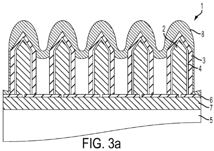
A p-electrode 8 in accordance with embodiments of the invention is at least
partly air-
bridged between adjacent nanowires 1. FIG. 3a schematically illustrates a p-
electrode 8
covering a group of nanowires 1. As noted above, if the shell 3 of the
nanowires 1 is n-type,
then electrode 8 would be an n-electrode. However, electrode 8 is referred to
herein as p-
electrode for ease of description. The p-electrode 8 is free-hanging between
adjacent
nanowires 1 and is only supported by the nanowires 1. The p-electrode 8
encloses a top
portion of each nanowire 1 and thereby contacts the p-side of the nanowire LED
structure.
The p-electrode may extend down along the sides of peripheral nanowires, e.g.,
in order to
8
CA 02802539 2012-12-12
WO 2011/160051 PCT/US2011/040932
provide a connection to a pad arranged on the substrate 5 (as will be
described in more detail
below and as shown on the right and left edges of FIG. 3a).
Different additional layers may be deposited on the p-electrode. For example
layers that
improve electrical conductivity or coupling of light out from/into the
nanowire may be
deposited on the nanowire.
The nanowire LED structure of the embodiments of the present invention is
either
adapted for top emitting, i.e., light emission through the p-electrode, or
bottom emitting, i.e.,
light emission through the support layer (i.e., through the conductive layer
and/or buffer layer
and/or substrate). The requirements on the p-electrode are different for these
two cases. As
used herein, the term light emission includes both visible light (e.g., blue
or violet light) as
well as UV or IR radiation.
For a top emitting device, the p-electrode needs to be transparent (i.e., it
should transmit
the majority of light emitted by the LED). Indium Tin Oxide (ITO) is a
suitable material for
the p-electrode, in particular for the top emitting nanowire LED. The ITO
preferably has a
thickness of 150-900nm, more preferably 250-650nm, most preferably about
500nm. ITO has
been extensively used also for planar components where LED devices are formed
by layer-
by-layer techniques. In such components the thickness of the ITO layer is
preferably about
150nm since this is enough to obtain an acceptable current spreading. One
drawback with
increased thickness is that the ITO has comparatively high absorption of
light. Therefore the
ITO thickness is kept as low as possible. Another reason for keeping the ITO
thickness low is
that the ITO cannot readily be wet etched if too thick, i.e. more than 150nm.
Surprisingly the
optimal ITO thickness for the p-electrode in accordance with the embodiments
of then
present invention is high. This can be explained by the fact that the
efficiency of the nanowire
LED is determined by a trade-off between good light coupling, i.e.
comparatively thick ITO,
and low absorption, i.e. comparatively thin ITO. The ITO can also be combined
with layers
of other materials to obtain specific properties. For example, similar
properties as when
having a 500nm ITO can be obtained by having a 150nm ITO covered with a
silicon oxide
layer. A thick p-electrode, preferably uniformly thick, will also contribute
to efficient heat
dissipation.
Other suitable materials for a p-electrode on a top emitting device are ZnO,
doped ZnO
and other transparent conducting oxides (TCOs). Important parameters for this
material are
9
CA 02802539 2012-12-12
WO 2011/160051 PCT/US2011/040932
good transparency, electrical conductivity and the ability to make low
resistive contact to the
shell. High thermal conductivity is also desirable, together with a matching
refractive index
(depending on configuration).
In one embodiment of a top emitting nanostructured LED the substrate is
provided with
a reflecting means (e.g., mirror) that preferably extends in a plane under the
nanowire LEDs.
For a bottom emitting LED, the p-electrode is preferably reflective. As shown
in the
following examples, the p-electrode may comprise one or more additional layers
deposited on
the p-electrode for improving the reflective and/or conductive properties.
FIG. 3b schematically illustrates one embodiment of a nanowire LED structure
in
accordance with embodiments of the invention. In principle it is the same
structure as shown
in FIG. 3a, but the p-electrode comprises a comparatively thin conductive
layer 8' enclosing
the p-type shell 3 and a comparatively thick air-bridged conductive layer 8"
arranged on the
thin conductive layer 8'. The thin conductive layer 8' extends down towards
the base of the
nanowire 1, longer than the thick conductive layer 8". The thin conductive
layer 8' can for
example be deposited using atomic layer deposition or grown as an epitaxial
layer on the p-
type shell. Layer 8' may be discontinuous between adjacent nanowires and may
cover only
the nanowires but not the masking layer 6 or buffer layer 7 between the
nanowires. With this
arrangement the thin conductive layer 8' can be used to obtain an optimal
interface to the p-
type shell 3 and the thick conductive layer 8" can be optimised for current
spreading and/or
light coupling and/or reflection. Thus, only layer 8" may be used to form the
air-bridge.
In an alternative embodiment, in addition to the mask layer 6, the space
between the
nanowires can also be filled fully or partially with a dielectric (i.e.,
insulating) material, such
as silicon oxide. For partially filled space, the air gap size below the air-
bridge is reduced.
For fully filled space, there is no longer an air-bridge. Thus, for the
embodiments described
below with regard to the contact schemes for the nanowires, it should be
understood than the
nanowires may be contacted either in an air-bridged or non-air-bridged
configurations.
In the following first implementation of a method for forming a top emitting
nanowire LED
structure is described with reference to FIGs. 4a-h. In this embodiment, the
same conductive
layer is patterned to form both the p and n electrode layers. In this
implementation, pads for
connecting to the n-side and p-side of the device are formed in pad areas
adjacent to the
CA 02802539 2012-12-12
WO 2011/160051 PCT/US2011/040932
nanowires forming the nanowire LED. However, the invention is not limited to
this
configuration.
FIG. 4a shows an array of nanowires 1 grown from a buffer layer 7 through a
growth
masking layer 6. The nanowires preferably comprise an n-type nanowire core 2
enclosed in a p-
type shell layer 3 with an intermediate active layer 4 for light generation,
as shown in FIG. 1.
The growth mask 6 may be patterned by photolithography to define openings for
the nanowire
growth, as described for example in U.S. Patent Number 7,829,443. In this
implementation,
the nanowires are grouped in an n-pad area, a non-active area, a LED area
(i.e., the area which
emits light) and a p-pad area. However, embodiments of the invention are not
limited to this.
For example the p-pad area may be arranged on top of the nanowires forming the
light emitting
part of the nanowire LED structure, whereby the p-pad area and the LED area
coincide, as
described in PCT International Application Publication Number WO 2010/014032
Al to
Konsek, et al., published February 4, 2010 and incorporated herein by
reference in its entirety.
Referring to FIG. 4b, in the next step a protection layer 9 is deposited, at
least in the
LED-area where the nanowires will form LEDs, to protect nanowires from the
subsequent
processing. Otherwise residuals from photoresist and reactive ions from
sputtering and
reactive ion etching (RIE) may cause defects and/or contamination. ZnO
deposited with
atomic layer deposition (ALD) can be used as a protection layer. One advantage
with ALD as
a deposition technique is its perfect step coverage. Other materials such as
other metal or
silicon oxides, e.g., A1203 or Si02, deposited with ALD or other deposition
techniques can
also be used. This layer may fill an additional role as insulator on areas
where it will be left.
Protection layer 9 deposition is followed by opening up, through lithography
and
etching, to the buffer layer 7 through the protection layer and the growth
mask in the n-pad
area 11. In other words, as shown in FIG. 4b, a photoresist or another masking
layer (shown
as dashed lines 12) is formed over the entire device and then removed in the n-
pad area 11 by
photolithography. The exposed protection layer 9 and the exposed masking layer
6 between
the nanowires 1 are etched by any suitable etching method which can stop on
the buffer layer
(e.g., any wet or dry etching method which can etch a metal oxide or silicon
oxide selectively
with respect to a Ill-nitride semiconductor buffer layer). The purpose is to
access the buffer
layer 7 for arranging an electrode thereon, in order to provide an electrical
connection
through the buffer layer 7 to the n-side of the nanowires 1 (i.e., an
electrical connection
through n-type layer 7 to n-type nanowire cores 2).
11
CA 02802539 2012-12-12
WO 2011/160051 PCT/US2011/040932
Referring to FIG. 4c, the next step is to form a sacrificial layer 10, such as
a photoresist
or another suitable sacrificial material layer, with two different thicknesses
extending over
the non-active area and the p-pad area. The photoresist layer should
completely cover the
nanowires in the non-active area 13, whereas it should partly cover the
nanowires 1 in the
LED area 14, leaving a top portion of each nanowire 1 in the LED area 14
exposed. If the
same contact materials are to be used in the n- and p- electrodes, areas which
should be
accessed as contact pads, i.e., the n-pad area 11 and the p-pad area 15, the n-
pad area is 11
preferably not covered by photoresist. This is clearly seen in the left part
of Fig. 4c. As
appreciated by one skilled in the art, this photoresist layer can be formed
e.g. by depositing
photoresist, and using two masks and two exposures and then development, or
larger
amplitude exposure in area 14 than in area 13 for a positive photoresist (or
vice versa for
negative photoresist). Also, the photoresist can comprise multiple layers
(e.g., forming,
exposing and developing a first resist in areas 13 and 14 and then forming,
exposing and
developing a second resist only in area 13 over the first resist). If desired,
the photoresist 10
may comprise a portion of the photoresist layer 12 used in FIG. 4b to pattern
layers 9 and 6.
In this case, photoresist layer 12 is exposed a second time using the methods
described above
in areas 14 and 15 but not in area 13 (or vice versa for a negative
photoresist), and then
developed (i.e., removed) fully in area 15 and partially in area 14.
Referring to FIG. 4d, the next step is to remove the protection layer 9 on at
least the
exposed top portions of the nanowires in the LED area 14 that are exposed
outside of
photoresist pattern 10. This may be done by selective etching which
selectively etches the
oxide protective layer 9 but not the masking layer 6 (e.g., silicon nitride)
or the
semiconductor buffer layer 7 or semiconductor nanowires 1. If desired, layer 9
may be left
in areas where it does not interfere in a contact between the semiconductor
material and a
respective electrode to provide additional electrical insulation on top of the
masking layer 6.
For example, an aluminium oxide layer may be used as such a permanent
protective layer 9
in combination with silicon nitride masking layer 6.
Thereafter the p-electrode layer 16 is deposited. Since the p-electrode
becomes elevated
and does not have to extend down deeply into the narrow space between the
nanowires 1,
line-of-sight processes such as sputtering or evaporation can be used. Of
course the n-
electrode layer is formed at the same time since the n-pad area 11 is exposed.
It should be
noted that p-electrode 16 does not contact the n-type buffer layer 7 in the p-
pad area 15
12
CA 02802539 2012-12-12
WO 2011/160051 PCT/US2011/040932
because the buffer layer 7 is covered by the masking layer 6 in the p-pad
area. Thus, a short
circuit between the p-electrode and the n-buffer layer / n-nanowire cores is
avoided.
However, if the left side portion of layer 16 is used to form the n-electrode,
then it this
portion of layer 16 contacts the exposed buffer layer 7 between the nanowires
in the n-pad
area 11. It should be noted that layer 16 does not contact the nanowires 1 in
the non-active
area 13 which is covered by the photoresist 13.
Referring to FIG. 4e, next step is to do another lithography step leaving
another
photoresist pattern 17 in the p-pad area 15, the LED area 14 and the n-pad
area 11. This may
be done by forming another photoresist layer over the device shown in FIG. 4d
(including
over the metal electrode 16 covered resist pattern 10 in non-active area 13)
and then exposing
and developing the photoresist to leave the photoresist pattern 17 on both
sides of the metal
electrode 16 covered resist pattern 10.
Referring to Fig. 4f, the next step is to remove the electrode material 16 on
the areas
where electrode material is not covered by resist pattern 17 from the previous
step, i.e., in the
non-active area 13, which can be done by selective dry or wet etching which
does not remove
the photoresist patterns 10 and 17. This causes the electrode layer 16 to
become
discontinuous such that it is removed in the non-active area 13 between the n-
pad area 11 and
the active and p-pad areas 14, 15.
Referring to Fig. 4g, next step is removal of all remaining photoresist 10,
17, which can
be done by dissolving and/or plasma etching. This leaves the p-electrode layer
16 free-
hanging between the nanowires 1 in the LED area 14. This forms the air-bridge
with empty
space 18 between the electrode 16, nanowires 1 and the masking layer 6.
Referring to Fig. 4h, finally residues of the protective layer 9 on the non-
active area 13
that still may be present is removed. Thus, layer 16 forms the p-electrode 16a
which contacts
the tips of the nanowire 1 p-shells 3 and contacts the masking layer 6 in the
p-pad area, as
well as the n-electrode 16b which contacts the n-buffer layer 7 in the n-pad
area 11. FIG. 5
shows two scanning electron microscope images of an air-bridged p-electrode in
accordance
with this embodiment of the invention. The intersection between the non-active
area and
LED area with the air-bridged p-electrode is visible on the left.
Since layer 16 was removed in non-active area 13, the same layer 16 may be
used to
form both p- and n-electrodes. Thus, in the above process sequence illustrated
by Figs. 4a to
13
CA 02802539 2012-12-12
WO 2011/160051 PCT/US2011/040932
4h, the p-electrode and n-electrode are deposited in the same step. The n-
electrode layer 16b
comprises an n-pad area 11 on a first part of the buffer layer 7. The p-
electrode layer 16a
comprises a p-pad area 15 on the nanowires in a LED active area 14 or on a
dielectric
masking layer 6 on the buffer layer 7 adjacent to the nanowires in the LED
active area. The
n-pad area and the p-pad area are separated by a non active area 13 comprising
dummy
nanowires 1 which do not contact the p-electrode (i.e., these nanowires do not
emit light).
However, in an alternative second embodiment, the p-electrode is provided in a
first step
and the n-electrode is formed from a different material at a later stage. Such
a process is
discloses in Figs. 4i to 4s and will be briefly described below. The
description of the same
elements and steps from Figs. 4a-4h will not be repeated below for brevity.
The first two steps in the second embodiment method are identical to the first
embodiment method, i.e. Figs 4a and b represent the same steps as Figs. 4i and
j. However,
the protective layer 9 and masking layer 6 are not removed in the n-pad area
11 Fig. 4j as in
Fig. 4b.
In the next step, a sacrificial (e.g., resist) layer 10a is deposited in two
different
thicknesses such that no nanowires are left uncovered in the n-pad area 11 as
in the first
embodiment. Thus, in the left hand side of Fig. 4k it can be seen that the
nanowires in area 11
are entirely covered just as the central nanowires in the non-active region
13, as opposed to in
Fig. 4c where the leftmost nanowires in n-pad area 11 are completely
uncovered. The
nanowires in the LED area 14 are partially exposed on the top in the
photoresist 10a. The p-
pad area 15 is completely exposed in photoresist pattern 10a.
Fig. 41 shows that the protective layer 9 is at least partially removed from
the exposed
nanowire tips in LED area 13 in order to provide for contact between the p-
shell 3 of the
nanowires in area 13 and the p-electrode.
The p-electrode layer 16 is then deposited as shown in Fig. 4m. Layer 16
covers the
entire structure. The inactive 13 and n-contact 11 areas are now covered by
the photoresist
10a and layer 16 is formed on top of the photoresist 10a. Layer 16 contacts
the exposed p-
shells 3 of the nanowires in LED area 14 and the masking layer 6 in the p-pad
area 15.
14
CA 02802539 2012-12-12
WO 2011/160051 PCT/US2011/040932
As shown in Fig. 4n, a second photoresist pattern 17a is now provided over the
p-
electrode layer 16 in the LED area 14 and the p-pad area 15. Photoresist
pattern 17a is
removed in areas 13 and 11. Thus, layer 16 is exposed in areas 11 and 13.
The exposed p-electrode layer 16 is then removed from areas 11 and 13 by
selective
etching, as shown in Fig. 4o.
As shown in Fig. 4p, all photoresist 10a, 17a is removed such that the p-
electrode layer
16 forms an air-bridge with underlying empty spaces 18 between the nanowires
in LED area
14, and forms a p-contact pad in area 15.
Next, a new photoresist pattern 19 is applied to cover areas 13, 14 and 15 but
not the n-
pad area 11, as can be seen in Fig. 4q. The protective layer 9 and masking
layer 6 are
removed from exposed area 11.
N-electrode layer 20 is then deposited over the entire structure, as shown in
Fig. 4r.
Layer 20 may comprise Ti and Al sublayers or any other suitable metal. Layer
20 contacts
the exposed buffer layer 7 and "dummy" shorted nanowires in area 11. Layer 20
rests on
photoresist 19 in areas 13, 14 and 15.
Fig. 4s shows a lift-off step in which the photoresist pattern 19 is removed
to lift off
layer 20 in areas 13, 14 and 15, such that the remaining layer 20 in area 11
forms the n-
electrode. There is no electrode layers 16, 20 in the non-active area 13. This
prevents
shorting of layer 16 and 20. Dummy nanowires are located in the non-active
area 13.
Figures 4h and 4s show in process devices prior to formation of contacts
(e.g., lead wires
or bump electrodes) to the p-electrode 16a, 16 and n-electrode 16b, 20,
respectively.
However, it should be understood that the contacts described with respect to
figures 6, 10 or
12 are made to the p-electrode in p-pad area 15 and the n-pad area 11,
respectively.
Furthermore, as noted above, the p-pad area 15 may be on top of nanowires
(e.g., areas 14
and 15 are combined) rather than between nanowires as shown in Figs. 4h and
4s.
The following third implementation of a method for forming a bottom emitting
nanowire
LED structure is described with reference to FIGs. 6a-h. In this
implementation pads for
connecting to the n-side and p-side are again formed in n-pad areas and p-pad
areas,
respectively, adjacent to the nanowires forming the nanowire LED. However, the
invention is
CA 02802539 2012-12-12
WO 2011/160051 PCT/US2011/040932
not limited to this. The same elements that were described above will not be
described again
below for brevity.
Fig. 6a shows the structure which is similar to Fig. 4a. As in the previously
described
with respect to Fig 4a, a photoresist layer or pattern 10b with two
thicknesses completely
covers nanowires in the non-active area 13 and partially encloses the
nanowires in the LED
area 14, leaving the top nanowire portions exposed. The n-pad area 11 and the
p-pad area 15
are open and not covered by the photoresist pattern 10b.
Referring to FIG. 6b, in a next step, the protective layer 9 on the exposed
top portion of
the nanowires in the LED area 14 is selectively removed. Then, a p-electrode
layer 16c, a
current spreading layer 16d and one or more reflector layers 16e are deposited
over the entire
device by for instance sputtering or evaporation. One or more of these layers
may be omitted
(e.g., the reflector layer 16d may be omitted if a separate mirror will be
used), as long as at
least one conductive layer is formed.
Referring to FIG. 6c, in a next step the photoresist 10b is removed to lift
off layers 16c,
16d and 16e, and is optionally followed by a heat treatment to tune the
properties of the
layers. This leaves layers 16c-16e in areas 11, 14 and 15. An air bridge is
formed in area 14
with empty spaces 18 described above. This separates layer 16c-e into p-
electrode 22 and n-
electrodes 23, as shown in FIG. 6d.
Referring to FIG. 6d, in next step, the residues of the protective layer 9, on
the non-
active area 13 is removed if desired.
Referring to FIG. 6e, in a next step solder ball bumps (SBB) (e.g., p-bump 21a
and n-
bump 21b) are attached to the p-pad 15 and n-pad 11 areas, respectively. In
the p-pad area
15, the p-electrode 22 is isolated from the n-buffer layer 7 by the masking
layer 6. The p-
electrode 22 provides electrical contact between the p-bump 21a and the p-
shells 3 in area 14.
The n-electrode 23 provides contact between n-bump 21b and the n-buffer layer
7 and n-
cores 2. Thus, the buffer layer is accessed by the n-electrode / n-bump and
the shells are
accessed by the p-electrode / p-bump to provide an external electrical
connection to the
LEDs.
Referring to FIG. 6f, in a next step the chip, i.e., the LED structure, is
flipped over and
dipped in a conductive adhesive 23 which remains on the bumps 21a, 21b. In
addition to
16
CA 02802539 2012-12-12
WO 2011/160051 PCT/US2011/040932
providing electrical conductivity, the conductive adhesive may improve the
heat dissipation
properties.
Referring to FIG. 6g, in a next step the chip is mounted on a carrier 24 pre-
processed
with p-and n-electrodes 25 and 26. Although described in terms of a SBB
arrangement it is
appreciated by a person skilled in the art that there are other contact
alternatives, such as lead
wire or lead frame connections.
Referring to FIG. 6h, in a next step, the space between the chip and the
carrier is
underfilled, for example by an epoxy material 27. The underfill provides
structural rigidity
and may also contribute to improved heat dissipation.
Referring to FIG. 6i, in a next step the Si substrate 5 is removed completely
or partially
by for example wet or dry etching to form an opening 28 exposing the buffer
layer 7. If
desired, the buffer layer 7 may also be removed through opening 28 to expose
the nanowire 1
bases.
FIG. 7 shows a nanowire structure obtained by this implementation of the
method with a
solder bump arranged on the nanowires. The p- and n-electrodes are accessed
via the carrier
wafer using a p-contact 29 and an n-contact 30. This forms a bottom emitting
LED device
which emits light from LED areas 14 through the buffer layer 7.
As mentioned above, nanowires may comprise heterostructures of compositionally
different materials, conductivity type and/or doping such as the above
exemplified radial
heterostructures forming the pn or pin junction. In addition, axial
heterostructures within the
nanowire core may also be formed. These axial heterostructures can form pn- or
p-i-n-
junctions that can be used for light generation in a nanowire LED. FIG. 8
schematically
illustrates a plurality of nanowires with axial pn-junctions (e.g., the p-
portion 3 located above
the n-portion 2 in the axial direction) contacted on the p-side 3 with an air-
bridge electrode 8
arrangement.
Although the present invention is described in terms of contacting of nanowire
LEDs, it
should be appreciated that other nanowire based semiconductor devices, such as
field-effect
transistors, diodes and, in particular, devices involving light absorption or
light generation,
such as, photodetectors, solar cells, lasers, etc., can be contacted in the
same way, and in
particular the air-bridge arrangement can be implemented on any nanowire
structures.
17
CA 02802539 2012-12-12
WO 2011/160051 PCT/US2011/040932
All references to top, bottom, base, lateral, etc are introduced for the easy
of understanding
only, and should not be considered as limiting to specific orientation.
Furthermore, the
dimensions of the structures in the drawings are not necessarily to scale.
Further embodiments of the invention provide processes for packaging top
emitting LEDs
as disclosed above, and such processes will be described below with reference
to Figs. 9-12.
Reference is first made to Fig. 9, showing a top emitting nanowire LED
structure 90 having
a mirror 91 provided on the backside. Thus, as already mentioned, for top
emitting LEDs the p-
contact 92(6) is transparent, preferably made of TCO, conductive polymer or
thin metal and in
order to direct the emitted light through the top, a mirror is preferably
provided below.
In order to attach a mirror, different methods can be used. In one embodiment,
after the p-
contact 92 has been provided, an n-contact 93(20) is provided on selected n-
contact areas 11 on
the LED array on the tips of the nanowires and between the nanowires in
contact with the buffer
layer 96 in the selected area 11 to provide a base for later wire bonding. The
n-contact, suitably
made of Ti/Al or other conductors (e.g., transparent alternatives, such as
TCO), is deposited so
as to cover the entire nanowire 94(1) and down through the masking layer 95(6)
so as to contact
the buffer layer 96(7), whereby after suitable wire bonding can be applied to
the LED array. The
deposition of the n-contact can be performed by any deposition technique,
exemplified by
sputtering, thermal or e-beam evaporation and plating. In order to make
contact for the Ti/Al,
openings are made in the masking layer 95 by etching e.g., wet etching or by
dry etching (RIE).
In order to enable handling during the further processing of the array, a
temporary carrier C
is bonded to the p-contact side. The carrier is schematically shown in ghost
lines. This carrier is
suitably a silicon wafer, a ceramic substrate, or a glass or metal plate.
There are several methods
for achieving the bonding of the carrier, such as a product obtainable from
Brewer Science
called "Temporary wafer bonding" or contact bonding. Other alternatives are to
use photoresist,
BCB or some other polymer temporary adhesive material. The adhesive is coated
on the
components to be bonded and pressure (and optionally heating) is applied. When
the carrier is
attached, the original growth substrate 5 on which the nanowires were grown is
subjected to an
etching procedure to provide a recess 97, such as an opening, depression or
full removal of the
growth substrate down to the GaN / AlGaN buffer layer, i.e. on the back side
of the array. The
width of the recess is indicated by the bracket. Etching is suitably by dry
etching, e.g., the so
18
CA 02802539 2012-12-12
WO 2011/160051 PCT/US2011/040932
called Bosch Process, well known to the skilled artisan. It is also possible
to use wet chemical
methods or a combination of grinding and etching.
A further step of removing (partly or entirely) the GaN/AlGaN buffer layer and
replacing it
with a conductive layer (e.g., 91) can optionally be made at this point. In
top emitting
applications this layer can preferably comprise a mirror, but should be
transparent for bottom
emitting applications.
If, the growth substrate is only partly removed, in order to protect the areas
of the substrate
which should not form the depression, suitable masks (e.g., photoresist) are
applied, depending
on the etch method used.
The mirror 91 is provided in the recess 97 for a top emitting LED. If desired,
plural mirrors
may be formed in plural recesses in the substrate. The provision of the mirror
can be performed
in several different ways. A preferred method is by sputtering Ag into the
recess 97 to a
thickness of about 1 m. Thicker layers improve thermal conductivity but
usually do not
improve reflectivity appreciably. Alternatively methods such as thermal or e-
beam evaporation
or plating can be used. This mirror can be passive in the sense that it is not
electrically active in
the array. The mirror simply reflects light out from the array to the top of
the nanowires. It can
also be active, but then additional steps, such as thinning of resistive
layers should be made if the
buffer ends with a material such as AlGaN.
After the mirror has been provided the recess 97 is filled up with a filler
material 98, e.g.
epoxy or other suitable heat conductive material, preferably of high
mechanical strength, so as to
provide structural rigidity. Other appropriate materials are exemplified by,
but not limited to
TiN, graphene, and other polycrystalline or amorphous carbon films. Such
materials may be
most suitable in cases where the growth substrate is fully removed, as
deposition times may be a
constraint when used in deep recess structures. Then, the entire structure is
debonded from the
temporary carrier C to arrive at the structure shown in Fig. 9.
The structure thus obtained is mounted to a suitable mount structure or
carrier 100, as
shown in Fig. 10. The mount structure surface may comprise layers to enhance
adhesion or
improve thermal properties of the device such as metals, TiN, graphene, and
other
polycrystalline or amorphous carbon films. Contacts pads, preferably gold or
other conductive
materials 101 are deposited on the n-contact areas to provide a bond pad for
wire bonding. Wires
102, such as gold or other wires are then attached between the mount 100 and
pad 101. Solder
19
CA 02802539 2012-12-12
WO 2011/160051 PCT/US2011/040932
bumps or bonds may be used to secure the wire 102 in place. At least one p-
contact pad 103 is
also provided on the p-electrode and wire 104 bonding is also made to this
contact from the
mount 100. Finally, there is provided a protective "bulb" or package 105 over
the exposed
LEDs, suitably of a silicone material.
Now, with reference to Fig. 11, a variant for the provision of a passive
mirror is shown. P-
and n-contacts 92, 93, respectively, are provided as described above with
respect to Figure 9,
and a temporary carrier C is also attached in the same manner. However, after
the temporary
carrier has been provided, the original substrate 5 is removed, suitably by
etching, although
methods such as polishing or grinding could be used too.
After the removal of the substrate so as to expose the buffer layer (e.g.,
AlGaN) 7, a mirror
111 is provided on the buffer layer 7. Suitably an Ag mirror is provided by
sputtering. Then, the
assembly is glue bonded to a new substrate 112, preferably using any of
silicone, epoxy, BCB or
other types of polymer 113 as adhesive. Finally, the carrier C is removed.
The same process steps as in the previous embodiment are used to make
contacts, wire
bonding and the protective "bulb" 105, as shown in Fig. 12.
In a variation of the process just described in connection with Figs. 11 and
12, the same
process is used except that instead of applying/attaching a mirror to the
buffer layer, instead the
mirror 111 is applied to a new substrate 112. Then the assembly of new
substrate and mirror is
attached to the buffer layer of the LED array structure by glue bonding. This
of course requires
that the adhesive is practically fully transparent in order that undue losses
will not occur. The
adhesive 113 in this case is located between the mirror 111 and the buffer
layer 7. In these
embodiments, the mirror 91, 111 is used as the support for the nanowires 1 in
addition to and/or
instead of the substrate 5 and/or buffer layer 7.
While the invention has been described in connection with what is presently
considered to
be the most practical and preferred embodiments, it is to be understood that
the invention is not
to be limited to the disclosed embodiments, on the contrary, it is intended to
cover various
modifications and equivalent arrangements within the scope of the appended
claims.