Note: Descriptions are shown in the official language in which they were submitted.
CA 02802666 2012-12-13
[DESCRIPTION]
[Title of Invention]
IMAGE PROCESSING DEVICE
[Technical Field]
[0001]
The present invention relates to an image processing device
that improves access efficiency of SDRAM in processing of
data of pixels each having the number of bits which is
non-power-of-two, while using the pixels in image
processing efficiently.
[Background Art]
[0002]
As a conventional technology for converting 16-bits and
10-bits, there has been known Patent Literature 1. When
the conventional technology is applied to a burst access
of SDRAM, a cell of 12-pixels (e.g., 3x4) is obtained from
one burst access. In order to dispose cells such that they
fill an image block of 8x8 pixels which is a unit in image
processing and is frequently used in image compression,
6-cells are required. In this case, data of 8-pixels is
not used in the image processing of the block of 8x8 pixels
to be wasted. This decreases access efficiency. In the
case of this example, since it accesses 72-pixels for
64-pixels, access efficiency is about 89%. Further, if one
pixel has 10-bits, since it accesses 128-bits for access
of 12 pixels (= 120-bits), access efficiency is about 94%.
1
CA 02802666 2012-12-13
Nearly, access efficiency becomes about 88%.
[0003]
The access efficiency of 89% is inadequate, and it is
desirable that the access efficiency becomes closer to 100%
by improving it to the extent possible.
[Citation List]
[Patent Literature]
[0004]
[PTL 1]
Japanese Patent Application Laid-Open Publication No.
2001-144716
[Summary of Invention]
[Technical Problem]
[0005]
The present invention is made in view of the above problem,
and it is an object thereof to provide an image processing
device that improves access efficiency of SDRAM in
processing of data of pixels each having the number of bits
which is non-power-of-two, while using the pixels in image
processing efficiently.
[Solution to Problem]
[0006]
In order to solve the above problem, an image processing
device according to the present invention includes: an
image processor that processes data related to an image;
and a memory that stores therein data before or after
2
CA 02802666 2012-12-13
processing, wherein a region corresponding to a processing
unit in the image by the image processor is defined as a
block, a region smaller than the block corresponding to a
transfer unit of data of the memory in the image is defined
as a cell, and when one or more blocks and two or more cells
are arranged along a scanning direction of the image, both
ends of them in the scanning direction are aligned.
[Advantageous Effects of Invention]
[0007]
According to the present invention, it is possible to
improve access efficiency of SDRAM in processing of data
of pixels each having the number of bits which is
non-power-of-two, while using the pixels in image
processing with economy.
[Brief Description of Drawings]
[0008]
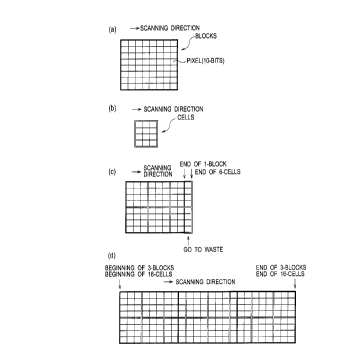
[FIG. 1]
It is a diagram that illustrates a positional relation
between a block and a cell included in an image of an image
processing device according to an exemplary embodiment of
the present invention.
[FIG. 2]
It is a diagram that illustrates another example related
to a shape and a size of a block according to the exemplary
embodiment of the present invention.
[FIG. 3]
3
CA 02802666 2012-12-13
It is a block diagram that illustrates a configuration of
the image processing device according to the exemplary
embodiment of the present invention.
[FIG. 4]
It is a diagram that illustrates a portion of the image
processing device according to the exemplary embodiment of
the present invention in detail.
[FIG. 5]
It is a flowchart when data is read from SDRAM according
to the exemplary embodiment of the present invention.
[FIG. 6]
It is a flowchart when data is written into SDRAM according
to the exemplary embodiment of the present invention.
[FIG. 7]
It is a timing chart when data is read from Banks A and B
of SDRAM according to the exemplary embodiment of the
present invention.
[FIG. 8]
It is a timing chart when data is written into Banks A and
B of SDRAM according to the exemplary embodiment of the
present invention.
[FIG. 9]
It is a diagram that illustrates a relation between data
of 16-bits and data of 40-bits to be read from or written
into SDRAM according to the exemplary embodiment of the
present invention.
4
CA 02802666 2012-12-13
[FIG. 10]
It is a diagram that illustrates a setting of address and
an order of a burst transfer of data according to the
exemplary embodiment of the present invention.
[FIG. 11]
It is a diagram that illustrates a flow of Read operation
in an efficient continuous burst access using clock cycles
in detail according to the exemplary embodiment of the
present invention.
[FIG. 12]
It is a diagram that illustrates a formation example of
image data in one frame when one word of SDRAM has 16-bits,
image data has 10-bits/pixel, and the amount of burst access
is 128-bits according to the exemplary embodiment of the
present invention.
[FIG. 13]
It is a timing chart when the image data structure of FIG.
12 is employed.
[FIG. 14]
It is a diagram that illustrates that an efficient
continuous burst access is realized even if a zigzag access
is carried out, according to the exemplary embodiment of
the present invention.
[Description of Embodiments]
[0009]
An exemplary embodiment of the present invention will be
5
CA 02802666 2012-12-13
described below with reference to drawings.
[0010]
FIG. 1 is a diagram that illustrates a positional relation
between a block and a cell included in an image of an image
processing device according to the present embodiment.
The image processing device according to the present
embodiment carries out processing in a unit of area (a block
shown in FIG. 1(a)) surrounded by 8-pixels in a scanning
direction (that is horizontal direction) and 8-pixels in
a vertical direction in an image which is composed of plural
pixels arranged in a matrix state. Data of 1-pixel has
10-bits.
[0011]
On the other hand, the image processing device includes
SDRAM (Synchronous Dynamic Random Access Memory). A word
which is a unit in reading/writing (collectively called
transfer) of SDRAM has 16-bits. In SDRAM, an 8-words
continuous transfer (burst access (burst transfer)) is
carried out. In one burst access, 128 (=16x 8) -bits are
transferred. In 128-
bits, data of 12-pixels (12 x10=
120-bits) is included. The 12-pixels is called a cell for
convenience.
[0012]
As shown in FIG. 1(b), the cell corresponds to an area
(12-pixels) surrounded by 3-pixels in the scanning
direction and 4-pixels in the vertical direction, for
6
CA 02802666 2012-12-13
example. In processing of 1-block, data of 64-pixels is
required. As shown in FIG. 1 (c) , if the cell has 12-pixels,
at least six burst transfers (12-pixels x 6-cells-data
transfer of 72-pixels) are required.
[0013]
Thus, as shown in FIG. 1 (c) , data of 8-pixels is not used
to go to waste in image processing of a block of 8x8 pixels.
This is because when 1-block and 6-cells are arranged in
the scanning direction, both ends of them can not be aligned
in the scanning direction.
[0014]
In view of the above, the image processing device carries
out processing in a processing unit of 3-blocks. In the
processing of 3-blocks, data of 192 (-64 x 3) -pixels is
required. This is a data amount corresponding to 16-cells.
As shown in FIG. 1 (d) , when 3-blocks and 16-cells are
arranged in the scanning direction of an image, both ends
of them in the scanning direction are aligned.
[0015]
Therefore, there is no data not used in image processing
as shown in FIG. 1 (c) . That is, access efficiency of SDRAM
is 100%.
[0016]
If the number of blocks for the processing unit is increased,
the volume of SRAM used in the image processing device needs
to be increased. So, it is preferable that the number of
7
CA 02802666 2012-12-13
blocks for the processing unit is 10 or less. It is noted
that the block is not limited to the area surrounded by
8-pixels in the scanning direction and 8-pixels in the
vertical direction.
[0017]
For example, the block may be an area surrounded by 8-pixels
in the scanning direction and 16-pixels in the vertical
direction as shown in FIG. 2(a), or an area surrounded by
16-pixels in the scanning direction and 8-pixels in the
vertical direction as shown in FIG. 2(b). This block is
composed of a luminance component (Y-component) area
surrounded by 8-pixels in the scanning direction and
8-pixels in the vertical direction, a chrominance component
(Cb-component) area surrounded by 4-pixels in the scanning
direction and 8-pixels in the vertical direction, and a
chrominance component (Cr-component) area surrounded by
4-pixels in the scanning direction and 8-pixels in the
vertical direction, for example. This arrangement is
called "4:2:2 chroma format".
[0018]
Alternately, the block may be an area surrounded by 8-pixels
in the scanning direction and 12-pixels in the vertical
direction as shown in FIG. 2(c), or an area surrounded by
12-pixels in the scanning direction and 8-pixels in the
vertical direction as shown in FIG. 2(d). This block is
composed of a luminance component (Y-component) area
8
CA 02802666 2012-12-13
surrounded by 8-pixels in the scanning direction and
8-pixels in the vertical direction, a chrominance component
(Cb-component) area surrounded by 4-pixels in the scanning
direction and 4-pixels in the vertical direction, and a
chrominance component (Cr-component) area surrounded by
4-pixels in the scanning direction and 4-pixels in the
vertical direction, for example. This arrangement is
called "4:2:0 chroma format". The cell is also not be
limited to 12-pixels.
[0019]
For example, data of 1-pixel may have 12-bits and the cell
has 10-pixels. If two SDRAMs are used to transfer 16-words
(256-bits) twice larger than one SDRAM in one burst access,
the number of pixels in the cell can be doubled.
[0020]
Thus, even if the size and/or shape of block and/or cell
are changed, access efficiency of SDRAM is increased by
carrying out the arrangement based on the above- described
rule.
[0021]
FIG. 3 is a block diagram that illustrates a configuration
of the image processing device. The image processing
device includes an image processor 1, SRAM 2, SDRAM 3, a
data selector unit DS, a shift register unit 4, a data
selector DS1, a counter 5, an SRAM address timing generator
6, an SRAM address generating table 7, an SDRAM signal
9
CA 02802666 2012-12-13
,
generator 8 and an SDRAM parameter setting unit 9.
[0022]
SRAM 2 is a working memory. Since SRAM easily carries out
a random access and realizes a medium-scale volume, SRAM
is used as a working memory in the image processing device.
[0023]
A buffer for SDRAM 3 includes SRAM 2 (working memory) and
the shift register unit 4 (arrangement of registers) .
[0024]
SDRAM 3 has Banks (e.g., eight banks A to H) , each of which
has the same size, which are obtained by dividing a memory
area into parts whose number is even.
[0025]
The SRAM address generating table 7 represents each
relation between a pixel position in an image and an address
in SDRAM 3 (Bank address, Row address and Column address) .
Namely, the SRAM address generating table 7 represents Bank
address, Row address and Column address on SDRAM in which
pixel data in each position is stored.
[0026]
The SDRAM parameter setting unit 9 is an element for setting
and controlling an access amount and a cell shape of SDRAM
3. The SDRAM parameter setting unit 9 is provided because
a different access control is required in an access for the
same 3-blocks due to a difference in block shapes for
luminance and chrominance or a difference in block shapes
CA 02802666 2012-12-13
,
for "4:4:2 format" and "4:2:0 format".
[0027]
FIG. 4 is a diagram that illustrates a portion of the image
processing device in detail. The data selector unit DS
includes data selectors DS2, DS3 and DS4. The shift
register unit 4 includes shift registers 4AB and 4CD.
[0028]
The data selector DS2 and the shift register 4AB are used
to access to Banks A, C, E and G. The data selector DS3
and the shift register 4CD are used to access to Banks B,
D, F and H.
[0029]
The shift register 4AB has a four stage shift register
composed of registers la, 2a, 3a and 4a and a four stage
shift register composed of registers lb, 2b, 3b and 4b.
[0030]
The shift register 4CD has a four stage shift register
composed of registers lc, 2c, 3c and 4c and a four stage
shift register composed of registers id, 2d, 3d and 4d.
[0031]
The data selectors DS2 and DS4 are connected to each other
via 40-bits bus. The data selectors DS3 and DS4 are also
connected to each other via 40-bits bus.
[0032]
Each of registers la, 2a, 3a, 4a, lb, 2b, 3b and 4b and the
data selector DS2 are connected to each other via 16-bits
11
CA 02802666 2012-12-13
,
, .
bus (total eight buses) . Each of registers lc, 2c, 3c, 4c,
ld, 2d, 3d and 4d and the data selector DS3 are also connected
to each other via 16-bits bus (total eight buses) .
[0033]
The registers la to 4a and the data selector DS1 are
connected to each other via 16-bits bus, clock signal Ra-CLK
and the like. The registers lb to 4b and the data selector
DS1 are connected to each other via 16-bits bus, clock
signal Rb-CLK and the like. The registers lc to 4c and the
data selector DS1 are connected to each other via 16-bits
bus, clock signal Rc-CLK and the like. The registers ld
to 4d and the data selector DS1 are connected to each other
via 16-bits bus, clock signal Rd-CLK and the like. The data
selector DS1 and SDRAM 3 are connected to each other via
a signal DQS, a signal DQSN (signal generated by delaying
signal DQS by half-clock cycle) and a 40-bits data signal
DQ.
[0034]
FIG. 5 is a flowchart when data is read from SDRAM. It is
here assumed that "the number of blocks necessary for
aligning the right end of blocks with the right end of cells"
in the explanation described with reference to FIG. 1 is
three.
[0035]
First, the SRAM address timing generator 6 calculates
addresses (Bank address, Row address and Column address)
12
CA 02802666 2012-12-13
of three blocks in SDRAM not subject to processing, with
reference to the SRAM address generating table 7 (Si)
[0036]
Next, data having the calculated addresses are read from
SDRAM 3 via the data selector DS1, the shift register unit
4 and the data selector unit DS and written to SRAM 2 (S3).
[0037]
At this time, the SDRAM signal generator 8 controls SDRAM
3 according to an access timing of SDRAM 3. At this time,
the SRAM address timing generator 6 carries out an access
control of SRAM 2. At this time, the data selector DS1,
the shift register unit 4 and the data selector unit DS
carries out arrangement conversion and temporal retention
of data of SRAM 2. The SDRAM signal generator 8 controls
SDRAM 3 and carries out the arrangement conversion and the
control of temporal retention. The SDRAM parameter
setting unit 9 sets and controls an access amount and a cell
shape of SDRAM 3.
[0038]
Next, the counter 5 is initialized to have the value "0"
(S5). Next, the image processor 1 reads from SRAM 2 data
of one block to be processed (S7). At this time, the SRAM
address timing generator 6 generates an access control
signal for reading.
Next, the image processor 1 processes the data of one block
(S9).
13
CA 02802666 2012-12-13
[0039]
Next, the value "1" is added to the counter 5 (S11). Next,
it is determined whether or not the counter 5 has the value
"3" (S13). If it is determined as NO, the processing
returns to step S7. If it is determined as YES, the
processing returns to step Si.
[0040]
It is noted that in order to efficiently access SDRAM, two
image processing devices carry out parallel processing of
this flowchart such that the timing of one processing
differs from the timing of the other processing.
[0041]
FIG. 6 is a flowchart when data is written into SDRAM. It
is also here assumed that "the number of blocks necessary
for aligning the right end of blocks with the right end of
cells" in the explanation described with reference to FIG.
1 is three.
[0042]
The counter 5 is initialized to have the value "0" (S21).
Next, the image processor 1 processes data of one block to
be processed (S23).
[0043]
Next, the image processor 1 writes the data into SRAM 2 (S25).
At this time, the SRAM address timing generator 6 generates
an access control signal for writing.
[0044]
14
CA 02802666 2012-12-13
Next, the value "1" is added to the counter 5 (S27). Next,
it is determined whether or not the counter 5 has the value
"3" (S29). If it is determined as NO, the processing
returns to step S23.
[0045]
If it is determined as YES, the SRAM address timing
generator 6 calculates addresses (Bank address, Row address
and Column address) of three blocks processed with
reference to the SRAM address generating table 7 (S31).
[0046]
Next, the data of three blocks processed is written to the
calculated positions in SDRAM 3 from SRAM 2 via the data
selector unit DS, the shift register unit 4 and the data
selector DS1 (S33), and then the processing returns to step
S21.
[0047]
At this time, the SDRAM signal generator 8 controls SDRAM
3 according to the access timing of SDRAM 3. At this time,
the SRAM address timing generator 6 carries out the access
control of SRAM 2. At this time, the data selector DS1,
the shift register unit 4 and the data selector unit DS
carries out the arrangement conversion and the temporal
retention of data of SRAM 2. The SDRAM signal generator
8 controls SDRAM 3 and carries out the arrangement
conversion and the control of temporal retention. The
SDRAM parameter setting unit 9 sets and controls the access
CA 02802666 2012-12-13
amount and the cell shape of SDRAM 3.
[0048]
It is noted that the data selector unit DS, the shift
register unit 4, the data selector DS1, the SDRAM signal
generator 8 and the SDRAM parameter setting unit 9 of the
image processing apparatus carry out parallel processing
while causing the timing of one Bank access to differ from
the timing of the other Bank access in two subsequent Bank
accesses of SDRAM so as to reduce an idle time of SDRAM.
[0049]
FIG. 7 is a timing chart when data is read from Bank A and
B of SDRAM.
[0050]
First, the data selector DS1 selects Bank A and reads from
SDRAM 3 using the bus signal DQ of 16 bits, data to be
transferred to the registers la to 4a and lb to 4b. Here,
data transfer of 16 bits is carries out eight successive
times.
[0051]
The data selector DS1 also transfers to the registers la
to 4a as a clock signal Ra-CLK in a selection time of Bank
A, a signal DQS output from SDRAM 3, and sends to the
registers la to 4a via the bus signal of 16-bits, data for
the registers la to 4a. The registers la to 4a obtain the
data in the timing of the clock signal Ra-CLK. Here, data
transfer is carried out four successive times (four data
16
CA 02802666 2012-12-13
,
transfers).
[0052]
The data selector DS 1 further transfers to the registers
lb to 4b as a clock signal Rb-CLK in the selection time of
Bank A, a signal DQSN output from SDRAM 3, and sends to the
registers lb to 4b via the bus signal of 16-bits, data for
the registers lb to 4b. The registers lb to 4b obtain the
data in the timing of the clock signal Rb-CLK. Here, data
transfer is carried out four successive times (remaining
four data transfers). Namely, four data transfers are
carried out in the registers la to 4a while four data
transfers which are delayed by a half clock are carried out
in the registers lb to 4b. Thus, total eight data transfers
are carried out as one burst access.
[0053]
Next, the data selector DS1 selects Bank B and reads from
SDRAM 3 using the bus signal DQ of 16 bits, data to be
transferred to the registers lc to 4c and ld to 4d. Here,
data transfer of 16 bits is carries out eight successive
times.
[0054]
The data selector DS1 also transfers to the registers lc
to 4c as a clock signal Rc-CLK in a selection time of Bank
B, a signal DQS output from SDRAM 3, and sends to the
registers lc to 4c via the bus signal of 16-bits, data for
the registers lc to 4c. The registers lc to 4c obtain the
17
CA 02802666 2012-12-13
data in the timing of the clock signal Rc-CLK. Here, data
transfer is carried out four successive times (four data
transfers).
[0055]
The data selector DS1 further transfers to the registers
id to 4d as a clock signal Rd-CLK in the selection time of
Bank B, a signal DQSN output from SDRAM 3, and sends to the
registers id to 4d via the bus signal of 16-bits, data for
the registers id to 4d. The registers id to 4d obtain the
data in the timing of the clock signal Rd-CLK. Here, data
transfer is carried out four successive times (remaining
four data transfers).
[0056]
Further, in the selection time of Bank B, the data selectors
DS2 and DS4 transfer data of the registers la to 4a and lb
to 4b to SRAM 2 via the bus signal of 40-bits. Here, data
transfer of 40-bits is carried out three times.
[0057]
Next, Bank A is selected, and the data selectors DS3 and
DS4 transfer to SRAM 2 via the bus signal of 40-bits, data
of the registers lc to 4c and ld to 4d while the registers
la to 4a and lb to 4b obtain next data.
[0058]
In the figure, SRAM-Ad represents an address signal of SRAM
at the time of writing data into SRAM 2. SRAM-WEN
represents a writing signal to SRAM at this time.
18
CA 02802666 2012-12-13
,
,
[0059]
Subsequently, the reading from Bank A via the registers la
to 4a and lb to 4b and the reading from Bank B via the
registers lc to 4c and ld to 4d are alternately performed
likewise.
[0060]
Thus, since the reading from Bank A is performed via the
registers la to 4a and lb to 4b, and the reading from Bank
B is performed via the registers lc to 4c and ld to 4d, they
are alternately performed. Therefore, the reading from
any one of Bank A, C, E and G and the reading from any one
of Bank B, D, F and H are alternately performed likewise.
[0061]
Also, while the shift register unit 4 reads data of one of
Banks A and B from SDRAM, it writes data of the other of
Banks A and B into SRAM, and thereby the reading from SFRAM
can be performed at high speed. By a similar reason, the
reading from Banks A, C, E and G and the reading from any
one of Banks B, D, F and H can be performed at high speed.
[0062]
FIG. 8 is a timing chart when data is written into Bank A
and B of SDRAM
[0063]
First, the data selectors DS2 and DS4 transfer to the
registers la to 4a and lb to 4b according to the timing of
a signal Rab-Load, data to be sent from SRAM 2 via the bus
19
CA 02802666 2012-12-13
signal of 40-bits. Here, data transfer of 40-bits is
carried out three times.
[0064]
Next, the data selectors DS3 and DS4 transfer to the
registers lc to 4c and ld to 4d according to the timing of
a signal Rcd-Load, data to be sent from SRAM 2 via the bus
signal of 40-bits. Here, data transfer of 40-bits is
carried out three times.
[0065]
In figure, SRAM-Ad represents an address signal of SRAM at
the time of reading data from SRAM 2. SRAM-Data represents
a data signal at this time.
[0066]
Also, while the registers lc to 4c and ld to 4d obtain the
data in such a manner, the data selector DS1 selects Bank
A, transfers to SDRAM 3 as a device-to-SDRAM signal DQSw
while the signal DQS is an SDRAM-to-device signal, a clock
signal Raw-CLK (which is a device-to-SDRAM signal while the
clock signal Ra-CLK is an SDRAM-to-device signal) output
from the resisters la to 4a, and transfers data of the
registers la to 4a to SDRAM 3 using the bus signal DQ of
16-bits. Here data transfer of 16-bits is carried out four
times.
[0067]
Further, in the selection time of Bank A (that is, while
the registers lc to 4c and ld to 4d obtain the data), the
CA 02802666 2012-12-13
data selector DS1 transfers to SDRAM 3 as a device-to-SDRAM
signal DQSNw while the signal DQSN is an SDRAM-to-device
signal, a clock signal Rbw-CLK (which is a device-to-SDRAM
signal while the clock signal Ra-CLK is an SDRAM-to-device
signal) output from the resisters lb to 4b, and transfers
data of the registers lb to 4b to SDRAM 3 using the bus signal
DQ of 16-bits. Here data transfer of 16-bits is carried
out four times. Namely, four data transfers are carried
out in the registers la to 4a while four data transfers which
are delayed by a half clock are carried out in the registers
lb to 4b. Thus, total eight data transfers are carried out
as one burst access.
[0068]
Next, while the registers la to 4a and lb to 4b obtain next
data, the data selector DS1 selects Bank B and transfers
data of the registers lc to 4c and ld to 4d to SDRAM 3 via
the bus signals of 16-bits. Here, data transfer of 16-bits
is carried out eight times.
[0069]
Subsequently, the writing via the registers la to 4a and
lb to 4b and the writing via the registers lc to 4c and ld
to 4d are alternately performed likewise.
[0070]
Thus, since the writing into Bank A is performed via the
registers la to 4a and lb to 4b, and the writing into Bank
B is performed via the registers lc to 4c and ld to 4d, they
21
CA 02802666 2012-12-13
are alternately performed. Therefore, the writing into
any one of Bank A, C, E and G and the writing into any one
of Bank B, D, F and H are alternately performed likewise.
[0071]
Also, while the shift register unit 4 reads data of one of
Banks A and B from SDRAM, it writes data of the other of
Banks A and B into SRAM, and thereby the reading from SDRAM
can be performed at high speed. By a similar reason, the
reading from Banks A, C, E and G and the reading from any
one of Banks B, D, F and H can be performed at high speed.
[0072]
FIG. 9 is a diagram that illustrates a relation between data
of 16-bits and data of 40-bits to be read from or written
into SDRAM 3. In reading from SDRAM 3, a data conversion
having the following relation is carried out.
[0073]
First, the data selector DS1 reads 16-bits word from SDRAM
3 eight times, and causes the shift register 4AB to hold
them, for example. Namely, the data selector DS1 reads
128-bits composed of words Wa0 to Wa7, and causes the shift
register 4AB to hold them, for example.
[0074]
Next, the data selector unit DS writes into SRAM 2, data
having four 10-bits words held in the shift register 4AB
three times, for example. Namely, the data selector unit
DS converts the words Wa0 to Wa7 into 120-bits composed of
22
CA 02802666 2012-12-13
,
words WOO to W03, W10 to W13, W20 to W23 and W30 to W33,
and writes them into SRAM 2. Remained 8-bits are removed
in the shift register 4AB and the data selector unit DS,
for example.
[0075]
Next, the image processor 1 reads the words WOO to W03, W10
to W13 and W20 to W23 from SRAM 2.
[0076]
On the other hand, in writing into SDRAM 3, a data conversion
having the following relation is carried out.
[0077]
First, the image processor 1 writes into SRAM 2, 120-bits
composed of words WOO to W03, W10 to W13 and W20 to W23.
[0078]
Next, the data selector unit DS reads from SRAM 2, the words
WOO to W03, W10 to W13 and W20 to W23, and causes the shift
register 4AB to hold them, for example. Remained 8-bits
are added to the words WOO to W03, W10 to W13 and W20 to
W23.
[0079]
Next, the data selector DS1 converts into words Wal to Wa8
the 128-bits to which the 8-bits are added, and writes them
into SDRAM 3.
[0080]
(Summary of burst access of SDRAM)
A summary of burst access of SDRAM will be described with
23
CA 02802666 2012-12-13
reference to FIG. 10. It is noted that although each
command has a large duration in FIG. 10, it is one clock
width in practice.
[0081]
An inside structure of SDRAM is partitioned into plural
Banks (four to eight Banks in DDR3-SDRAM). For example,
when SDRAM of 2-Gbits is partitioned into eight Banks, one
Bank has a size of 256-Mbits. When a word width of this
SDRAM has 16-bits, since the number of words is 16M-words
(=256-Mbits/16-bits), the number of bits of address
assigned to each of 16M-words is 24-bits. The address of
24-bits includes Row address and Column address.
Therefore, in a case of accessing SDRAM, an address group
including Bank address, Row address and Column address is
required.
[0082]
In a first command Cmd-1, an address of Bank of an access
target and a desired Row address in Bank of the access target
are set in Active. In a second command Cmd-2, the address
of Bank of the access target, a start address of Column on
the desired Row address in Bank of the access target, and
Read/Write mode (including a bust access setting) are
designated after a predetermined time (Cmd-2 waiting time)
has elapsed from the time when the first command Cmd-1 is
issued. After a predetermined time (burst delay time) has
elapsed from the time when the second command Cmd-2 is
24
CA 02802666 2012-12-13
. ,
issued, Read or Write operation is carried out by a burst
access (8-words continuous transfer) from the designated
start address of Column as a stating point.
[0083]
(Method of effectively carrying out burst access of SDRAM)
A method of effectively carrying out a burst access of SDRAM
will be described with reference to FIG. 11.
[0084]
For example, when data of 32 words is arranged in SDRAM,
the data of 32 words is divided into four segments each
having 8-words and the four segments are respectively
arranged in four Bank A, B, C and D because it is impossible
to carry out a continuous burst access to different Row
addresses of the same Bank in SDRAM. When the data of 32
words arranged this way is read, first commands Cmd-1A,
Cmd-1B, Cmd-1C and Cmd-1D are initially issued and then
addresses of Banks A, B, C and D of access targets and desired
Row addresses in Bank A, B, C and D of the access targets
are set in Active (not shown in FIG. 11). Next, second
commands Cmd-2A, Cmd-2B, Cmd-2C and Cmd-2D are issued and
then the addresses of Banks A, B, C and D of the access
targets, start addresses (Xl, Y1 and the like) of Columns
on the desired Row addresses in Banks A, B, C and D of the
access targets, and Read modes are designated. Here, in
a case where duration of each command, duration of burst
delay time and duration of 8-words burst access are
CA 02802666 2012-12-13
. ,
,
respectively one clock, six clocks and four clocks, if the
second command is issued in every four clocks, the burst
access is effectively and continuously carried out (see FIG.
11).
[0085]
The Cmd-2 waiting time and the burst delay time are
previously determined as specification of SDRAM. In the
above-described example, if the Cmd-2 waiting time
coincides with a period until three first commands have been
issued, the second command Cmd-2A is issued after the first
commands Cmd-1A, Cmd-1B and Cmd-1C have been issued, so as
to effectively and continuously carry out the burst access.
Then, after the first command Cmd-1D has been issued, the
second commands Cmd-2B, Cmd-2C and Cmd-2D are issued.
[0086]
Generally, a delay from the issue of first command until
the start of its burst access requires about 12 clocks. In
continuous burst access, if Bank address and Row address
of an access target are not changed, the first commands
firstly issued can be commonly used. Thus, a delay from
the issue of second command until the start of its burst
access requires about eight clocks. In SDRAM, the first
command can be issued in every eight clock circles or less.
Thus, if 8-words burst accesses are continuously carried
out with respect to Banks differing from each other, the
most effective access with no gap is realized. Therefore,
26
CA 02802666 2012-12-13
in order to realize an access efficiency of SDRAM, (1) 8
words burst access is carried out with respect to a data
segment allocated in each Bank, (2) adjacent data segments
are allocated in Banks differing from each other, and (3)
when a continuous burst access is carried out with respect
to a large amount of data, the first commands are adeluately
issued to change the Bank and/or Raw address of an access
target.
[0087]
Thus, when the continuous burst access to Banks is carried
out based to optimal command scheduling, the maximum access
amount per unit time is realized. Also, by carrying out
similar processing at the time of Write operation, the
maximum access amount per unit time is realized.
[0088]
FIG. 12 is a diagram that illustrates a formation example
of image data in one frame in the case where the amount of
burst access is 128-bits when one word of SDRAM has 16-bits
and image data has 10-bits/pixel.
[0089]
Here, a cell has 3-pixels in a horizontal direction and
4-pixels in a vertical direction. It is desirable to
include descriptions of Bank address, Row address and
Column address in the cell.
[0090]
When 128-bits are represented by 10-bits/pixel, it divided
27
CA 02802666 2012-12-13
into 12-pixels (cell) . There are some options for the
geometric arrangement of 12-pixels, more specifically,
there are a total of six arrangement methods 1x12, 2x6,
3 x 4, 4x3, 6x2 and 12 x 1 (first number represents the number
of pixels in the horizontal direction and second number
represents the number of pixels in the vertical direction) .
In the drawing, RA represents Row address and CA represents
Column address.
[0091]
In FIG. 12, in each of the first row, the third row = = = ,
cells are repeatedly arranged in order of Banks A, B, C and
D and Column addresses are changed. If Column address
reaches the maximum value, Row addresses are changed and
cells are repeatedly arranged in order of Banks A, B, C and
D. In each of the second row, the four row = = = , cells are
repeatedly arranged in order of Banks E, F, G and H and Column
addresses are changed. If Column address reaches the
maximum value, Row addresses are changed and cells are
repeatedly arranged in order of Banks E, F, G and H and Column
addresses are changed. If Column address reaches the
maximum value, Row addresses are changed and cells are
repeatedly arranged in order of Banks E, F, G and H.
[0092]
In FIG. 12, an access along a line arrow in a hatching
rectangular region of 5x2 will be described. At the time
of shifting from a cell in an upper row to a cell in a lower
28
CA 02802666 2012-12-13
row, if both of the cells belong to the same Bank, a
continuous access can not be carried out. In order to avoid
a continuous access to the same Bank after shifting in the
vertical direction and allow a continuous access to a
different Bank after shifting in the vertical direction,
it is preferred to arrange eight Banks. Thus, even if Raw
address is changed, a continuous burst access can be carried
out because the arrangement of Banks in an upper row differs
from that in a lower row.
[0093]
Namely, a reason why eight Banks are alternately arranged
is as follows. If an alternate burst access to two or more
Banks is not carried out, the maximum access speed can not
be obtained. That is, since a gap occurs between bursts
in a continuous access to the same Bank, the maximum access
speed is not continuously realized.
[0094]
In an access in the same Column of a certain Bank, it is
necessary to change Row address because it has about 1024
words (16-Kbits) . At this time, since the change of Row
address needs a redundant time, it is necessary to use three
or more Banks alternately. By reason of easy control, it
is reasonable to use four Banks alternately in a circuit
configuration.
[0095]
At the time of accessing cells again after accessing cells
29
CA 02802666 2012-12-13
in the horizontal direction and then shifting by one cell
in the vertical direction, if different Banks are not
arranged, the maximum access speed is not realized. Thus,
four Banks are arranged in the horizontal direction in
sequence and two Banks are alternately arranged in the
vertical direction. In such arrangement, for any
rectangular region (plural block regions), a burst access
of SDRAM with the maximum access speed can be realized.
[0096]
FIG. 13 is a timing chart when the image data structure of
FIG. 12 is employed. FIG. 13 illustrates operations of
eight Banks and two pairs of register groups in Read
operation or Write operation along the line arrow in the
rectangular region of 5x2 cells in FIG. 12.
[0097]
In FIG. 13, at apart illustrated as "SRAM access", the data
transfer operation between SDRAM access buffer registers
(sorting registers) and input-and-output of the image
processing device are carried out. At the time of Read
operation of SDRAM, Read operation corresponds to SRAM
access after SDRAM access, and the read Bank data is
transferred to SRAM of the image processing device. At the
time of Write operation of SDRAM, it corresponds to SDRAM
access after SRAM access, and data from the image processing
device to be written subsequently is transferred from SRAM
of the image processing device to the SDRAM access buffer
CA 02802666 2012-12-13
register.
[0098]
As shown in FIG. 13, by alternately arranging eight cells,
a continuous burst access in order of Banks C, D, A, B, C,
G, H, E, F and G in the rectangular region of 5x2 can be
realized.
[0099]
It is noted that although one cell is formed by
3-pixelsx4-lines in FIG. 12, one burst access only need
to have 12-pixels (e.g., 6-pixelsx2-lines) .
[0100]
Further, in consideration of a color image, a method of
using all 12-pixels as luminance pixels or chrominance
pixels is possible for 4:2:2 chroma format. In this case,
different Banks may be used for a luminance signal and a
chrominance signal, and different Row addresses may be set
for a luminance and a chrominance. Also, 12-pixels may be
divided into 6-pixels for a luminance and 6-pixels for a
chrominance.
[0101]
In the present embodiment, one pixel is processed with
10-bits. If one pixel is processed with 12-bits, for
correspondence between a data width of 12-bits and a SDRAM
high speed burst access unit of 128-bits, it is assumed that
ten data widths of 12-bits are included in 128-bits.
[0102]
31
CA 02802666 2012-12-13
In this case, the formula "128-bits=12-bitsx10+8-bits" is
satisfied and remained 8-bits are deleted with no use of
it. In this case, an arrangement in an image memory has
lx10, 2x5, 5x2 or 10x1, and an optimal arrangement is
selected from them.
[0103]
When SDRAMs with two chips configuration are used in
parallel, a burst access unit has 256-bits. At this time,
there are a manner in which 256-bits is represented by
12-bits x21+4-bits and a manner in which 256-bits is
represented by 12-bitsx20+16-bits. If 21-pixels is used,
an arrangement in an image memory has 1x2 1 , 3x7, 7x3 or 2 lx1 .
If 20-pixels is used, an arrangement in an image memory has
1x20, 2x10, 4x5, 5x4, 10x2 or 20x1.
[0104]
As described above, even if a bit width used for accessing
a memory differs from a bit width used for accessing an image
processing device, the present embodiment can be applied.
[0105]
FIG. 14 illustrates that a continuous burst access with
efficiency is also realized by a zigzag access in place of
an access to an adjacent region in a horizontal direction
or a continuous access to an upper limit adjacent region
in a vertical direction.
[0106]
As described above, although the exemplary embodiment of
32
CA 02802666 2012-12-13
. .
the present invention has been described, as a more concrete
application field according to the above-described image
processing device, it is possible to configure an encoder
or a decoder compliant with "High 4:2:2 Profile" standard,
"High 10 Profile" standard or the like, which is
specifically directed to a high quality video, in ITU-T
Recommendation H.264 which is Motion Picture Coding
International Standard, at a low price.
[0107]
Use of SDRAM is essential for implementation of an encoder
or a decoder for motion picture. Recently, SDRAM is
developed in order of DDR, DDR2 and DDR3. A storage
capacity of current mainstream DDR3 SDRAM has about 1-Gbits
to 2Gbits. This capacity can store hi-vision images by 30
to 60 frames. Since the encoder or decoder of H.264 is
normally realized with a storage capacity having about 4
to 6 frames, recent SDRAM has enough capacity as a storage
requirement.
[0108]
On the other hand, it is not always sufficient for SDRAM
access. Due to this, in order to secure an access amount,
two to four SDRAMs are used while one SDRAM is sufficient
for storage capacity.
[0109]
Although a more high quality image can be obtained by
expanding each piece of image data from 8-bits to 10-bits,
33
CA 02802666 2012-12-13
,
an invention to increase access efficiency is required in
view of SDRAM. In addition, an operation speed of SDRAM
has a clock frequency of 500MHz or more and image signal
processing is carried out in parallel. The present
invention realizes an encoder and a decoder suitable for
such situation, and produces an effect for various image
signal processing applications (a medical image, a frame
frequency conversion, an image recognizing device and the
like).
[0110]
In order to store a high quality image for long periods,
HDD (Hard Disk Drive) is also an important storage. HDD
has a configuration of a conventional power-of-two value
unit, and an access speed for storage capacity of HDD
recently increases. For a high quality AV (Audiovisual)
application such as 10-bits video or 20-bits video, the
effect of the present invention is applied. Since DVD
(Digital Versatile Disk), BD (Blue-ray Disk) and the like
also have data configurations of a power-of-two value as
well as HDD, the effect of the present invention is applied
to realization of a high quality signal processing device.
[0111]
A sector size (about 2048-bites) of a digital storage medium
such as HDD, DVD or BD is larger than the burst size of SDRAM
described above. Thus, as well as SDRAM, a data
configuration of 8-bits unit (bite) may be converted into
34
CA 02802666 2012-12-13
,
a data configuration of 10-bits unit or 12-bits unit, for
every 128-bits (16-bites) or 256-bits (32-bites).
[Reference Signs List]
[0112]
1 image processor
2 SRAM
3 SDRAM
4 shift register unit
5 counter
6 SRAM address timing generator
7 SRAM address generating table
8 SDRAM signal generator
9 SDRAM parameter setting unit
DS data selector unit
DS1 to D54 data selectors
4A3, 4CD shift registers
la to 4a, lb to 4b, lc to 4c, ld to 4d registers