Note: Descriptions are shown in the official language in which they were submitted.
CA 02803304 2015-07-21
THERMAL CONTROL OF SOLID STATE LIGHT SOURCES BY VARIABLE
SERIES IMPEDANCE
CROSS-REFERENCE TO RELATED APPLICATION
[0001]
TECHNICAL FIELD
[0002] The present invention relates to lighting, and more specifically, to
electronic
control of solid state light sources.
BACKGROUND
[0003] A solid state light source, such as but not limited to a light emitting
diode
(LED) of any type (e.g., LED, OLED, PLED, etc.), is a current driven
electronic
device. Typically, one or more solid state light sources are driven by a
current
source, such as but not limited to a constant current source. A solid state
light
source, either alone or when located within a module such as a light engine,
may
additionally include an optical system (e.g., a lens) and/or an associated
wavelength-converting element, such as but not limited to a phosphor. These
additional elements, either separately or together, may convert the primary
light
output of the solid state light source to a secondary light output of a
different
wavelength/ color.
[0004] The light output level of the solid state light source may be adjusted
by
adjusting the output current of the constant current source using conventional
dimming techniques. For example, a light output level of a light engine
including
one or more solid state light sources may be adjusted by pulse-width-
modulation
(PWM) or amplitude modulation of the output current of the constant current
source, or by adjusting a steady state DC output of the constant current
source.
1
CA 02803304 2012-12-18
WO 2012/018915 PCT/US2011/046424
SUMMARY
[0005] One consideration in the design of a module including one or more solid
state
light sources is the heat generated by the module, and more particularly, by
the solid
state light sources. In some situations, it may be useful to at least
temporarily
remove power to a solid state light source module in the event the temperature
in a
region adjacent the module exceeds a threshold temperature. Thermal control
and/or thermal shutdown due to over-temperature conditions in a solid state
light
source module may be implemented using a conventional bi-metallic thermal
switch
positioned on a printed circuit board (PCB) attached to the solid state light
sources
and/or the module. The bi-metallic thermal switch is configured to open the
circuit
and cut power to the module in response to an over-temperature condition.
[0006] A conventional bi-metallic switch, however, may be bulky and thus may
occupy significant space within the module. In some designs, a solid state
light
source module may have a large amount of available space in which to
incorporate
such a switch. However, particularly in module designs where space is at a
premium, use of such a switch may not be practical. Further, regardless of
space
availability, such switches typically have a somewhat limited life in
comparison with
the expected lifetime of a lighting module including solid state light sources
such as
LEDs.
[0007] Embodiments of the present invention provide a thermal protection
circuit
that generally includes a temperature sensor, a variable impedance circuit,
and a
control circuit. The variable impedance circuit is coupled in series with a
current
source (e.g., a constant current source) and a plurality of solid state light
sources
(either separate from or as part of one or more modules). The thermal
protection
circuit is configured to control the variable impedance circuit based on the
sensed
temperature to reduce the current to the plurality of solid state light
sources. If the
sensed temperature exceeds a predetermined threshold temperature when a supply
voltage to the control circuit exceeds a minimum supply voltage of the control
circuit, the thermal protection circuit activates.
2
CA 02803304 2015-07-21
[0008] In some embodiments, the input voltage to the thermal protection
circuit is
provided by an output voltage of the current source (e.g., a constant current
source), which may vary depending on the impedance of the load driven by the
current source and/or a selected dimming input setting. At a low current
source
output voltage, e.g. resulting from a low dimmer setting, the input voltage to
the
thermal protection circuit may fall below a minimum supply voltage of at least
a
portion of the control circuit. The thermal protection circuit thus may
include a
low voltage compensation circuit configured to compensate for an input voltage
below a minimum supply voltage.
[0009] For example, the thermal protection circuit may be configured to drive
the
variable impedance circuit to a low impedance state, independent of the
control
circuit, when the input voltage falls below a low voltage threshold
corresponding
to the minimum supply voltage. This allows normal operation of the solid state
light sources at very low light output levels, for example as established by a
low
dimmer setting. The low voltage compensation circuit may be further configured
to compensate for effects of the variation in the input voltage on the supply
voltage to the control circuit. For example, the low voltage compensation
circuit
may include an energy storage element, e.g., a capacitor, configured to slow
the
decrease in the input voltage during dimming.
[0010] In an embodiment, there is provided a thermal protection circuit
comprising: a variable impedance circuit configured to be coupled to a
constant
current source and a plurality of solid state light sources, the constant
current
source configured to provide a current to the plurality of solid state light
sources
and to provide an output voltage to establish a supply voltage for the thermal
protection circuit; a temperature sensor configured to sense a temperature of
the
plurality of solid state light sources; a control circuit configured to
receive the
supply voltage and to drive the variable impedance circuit based on the sensed
temperature, to adjust the current to the plurality of solid state light
sources when
3
CA 02803304 2015-07-21
the supply voltage is a least a minimum supply voltage of the control circuit;
and a
low voltage compensation circuit configured to drive the variable impedance
circuit to a low impedance state when the supply voltage is below the minimum
supply voltage, independent of the sensed temperature.
[0011] In a related embodiment, the thermal protection circuit may further
include
a low voltage compensation circuit configured to drive the variable impedance
circuit to a low impedance state when the supply voltage is below the minimum
supply voltage, independent of the sensed temperature. In a further related
embodiment, the low voltage compensation circuit may include a low voltage
control circuit configured to isolate the control circuit from the variable
impedance
circuit when the supply voltage is below the minimum supply voltage. In
another
further related embodiment, the low voltage compensation circuit may include
an
energy storage element configured to maintain the supply voltage above the
minimum supply voltage for a time period after the output voltage decreases to
below the minimum supply voltage.
[0012] In another related embodiment, the control circuit may include a
temperature threshold circuit; and a comparator circuit; wherein the
comparator
circuit may be coupled to the temperature threshold circuit and the
temperature
sensor, and the comparator circuit may be configured to drive the variable
impedance circuit to a high impedance state when the sensed temperature is
greater than or equal to a predetermined threshold temperature. In a further
related embodiment, the comparator circuit may be configured to drive the
variable impedance circuit to an impedance between a high impedance state and
a
low impedance state based on a difference between the sensed temperature and a
pre-determined threshold temperature.
[0013] In yet another related embodiment, the plurality of solid state light
sources
may be located in a plurality of solid state light source modules.
4
CA 02803304 2015-07-21
[0014] In another embodiment, there is provided a thermal protection lighting
system comprising: a plurality of solid state light sources located in one or
more
solid state light source modules; a constant current source configured to
provide a
current to the plurality of solid state light sources and an output voltage to
establish a supply voltage; and a thermal protection circuit comprising: a
variable
impedance circuit coupled to the constant current source and the plurality of
solid
state light sources; a temperature sensor configured to sense a temperature of
the
plurality of solid state light sources; a control circuit configured to
receive the
supply voltage and to drive the variable impedance circuit based on the sensed
temperature to control the current to the plurality of solid state light
sources when
the supply voltage is a least a minimum supply voltage of the control circuit;
and
a low voltage compensation circuit configured to drive the variable impedance
circuit to a low impedance state when the supply voltage is below the minimum
supply voltage, independent of the sensed temperature.
[0015] In a related embodiment, the thermal protection circuit may include a
low
voltage compensation circuit configured to drive the variable impedance
circuit to
a low impedance state when the supply voltage is below the minimum supply
voltage, independent of the sensed temperature. In a further related
embodiment,
the low voltage compensation circuit may include a low voltage control circuit
configured to isolate the control circuit from the variable impedance circuit
when
the supply voltage is below the minimum supply voltage. In another further
related embodiment, the low voltage compensation circuit may include an energy
storage element configured to maintain the supply voltage above the minimum
supply voltage for a time period after the output voltage decreases to below
the
minimum supply voltage.
[0016] In another related embodiment, the control circuit may include: a
temperature threshold circuit; and a comparator circuit; wherein the
comparator
circuit may be coupled to the temperature threshold circuit and the
temperature
CA 02803304 2015-07-21
sensor, and the comparator circuit may be configured to drive the variable
impedance circuit to a high impedance state when the sensed temperature is
greater than or equal to a predetermined threshold temperature. In a further
related embodiment, the comparator circuit may be configured to drive the
variable impedance circuit to an impedance between a high impedance state and
a
low impedance state based on a difference between the sensed temperature and a
pre-determined threshold temperature.
[0017] In yet another related embodiment, the constant current source may be
configured to receive a dimming input signal and to provide the current to the
plurality of solid state light sources based on the dimming input.
[0018] In another embodiment, there is provided a method of providing thermal
protection, the method comprising: coupling a variable impedance circuit to a
constant current source and a plurality of solid state light sources, the
constant
current source configured to provide a current to the plurality of solid state
light
sources and to provide an output voltage to establish a supply voltage;
sensing a
temperature of the plurality of solid state light sources using a temperature
sensor;
and driving the variable impedance circuit by a control circuit, to adjust the
current to the plurality of solid state light sources when a supply voltage is
at least
a minimum supply voltage of the control circuit, wherein driving comprises
driving the variable impedance circuit to a low impedance state by a low
voltage
compensation circuit when the supply voltage is below the minimum supply
voltage, independent of the sensed temperature.
[0019] In a related embodiment, driving may include driving the variable
impedance circuit to a low impedance state by a low voltage compensation
circuit
when the supply voltage is below the minimum supply voltage, independent of
the sensed temperature. In a further related embodiment, the method may
further
include isolating the control circuit from the variable impedance circuit, via
a low
voltage control circuit, when the supply voltage is below the minimum supply
6
CA 02803304 2015-07-21
voltage, wherein the low voltage control circuit is part of the low voltage
compensation circuit. In another further related embodiment, the method may
further include maintaining, via an energy storage element of the low voltage
compensation circuit, the supply voltage above the minimum supply voltage for
a
time period after the output voltage decreases to below the minimum supply
voltage.
[0020] In another related embodiment, driving may include: driving the
variable
impedance circuit, via a comparator circuit of the control circuit, to a high
impedance state when the sensed temperature is greater than or equal to a
predetermined threshold temperature, wherein the comparator circuit is coupled
to a temperature threshold circuit and the temperature sensor. In a further
related
embodiment, driving may include driving the variable impedance circuit, via a
comparator circuit of the control circuit, to an impedance between a high
impedance state and a low impedance state based on a difference between the
sensed temperature and a pre-determined threshold temperature.
BRIEF DESCRIPTION OF THE DRAWINGS
[0021] The foregoing and other objects, features and advantages disclosed
herein
will be apparent from the following description of particular embodiments
disclosed herein, as illustrated in the accompanying drawings, in which like
reference characters refer to the same parts throughout the different views.
The
drawings are not necessarily to scale, emphasis instead being placed upon
illustrating the principles disclosed herein.
6a
CA 02803304 2012-12-18
WO 2012/018915 PCT/US2011/046424
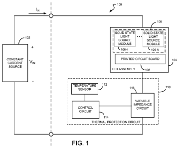
[0022] FIG. 1 shows a block diagram of a thermal protection lighting system
according to embodiments disclosed herein.
[0023] FIG. 2 is a block diagram of a control circuit of the thermal
protection lighting
system of FIG. 1.
[0024] FIG. 3 is a schematic diagram of a thermal protection lighting system
according to embodiments disclosed herein.
[0025] FIG. 4 a schematic diagram of a thermal protection lighting system
according
to embodiments disclosed herein.
[0026] FIG. 5 is a block diagram of a thermal protection lighting system
according to
embodiments disclosed herein.
[0027] FIG. 6 a schematic diagram of a thermal protection lighting system
according
to embodiments disclosed herein.
[0028] FIGs. 7- 9 show plots of exemplary input current TIN and input voltage
VIN
versus time for the system illustrated in FIG. 6 for PWM duty cycles of 98%,
50% and
4%, respectively.
[0029] FIG. 10 is a block flow diagram of a method according to embodiments
disclosed herein.
DETAILED DESCRIPTION
[0030] FIG. 1 is a block diagram of a thermal protection lighting system 100
(hereinafter system 100) according to embodiments described herein. The system
100 includes a constant current source 102, an LED assembly 104, and a thermal
protection circuit 110. The constant current source 102 may be a known current
source configured to supply a relatively constant current TIN to the LED
assembly 104
and a variable input voltage VIN to the system 100. The variable input voltage
VIN
from the constant current source 102 may be used to establish a supply voltage
for
operation of the thermal protection circuit 110.
[0031] The LED assembly 104 may include a plurality of solid state light
source
modules 106-1... 106-n, collectively solid state light source modules 106, and
a
printed circuit board (PCB) 108. Each solid state light source module 106-1 .
. . 106-n
7
CA 02803304 2012-12-18
WO 2012/018915 PCT/US2011/046424
includes at least one solid state light source. Thus, a solid state light
source module
106 may include a plurality of solid state lights sources. In some
embodiments, the
solid state light source modules 106 may be mounted on the printed circuit
board
(PCB) 108 or an equivalent substrate. In some embodiments (not shown in FIG.
1),
the constant current source 102 may be provided locally, e.g. on and/or in
connection with the same printed circuit board 108 as the LED assembly 104 or
the
thermal protection circuit 110, or may be positioned remotely therefrom, e.g.
on a
physically separate printed circuit board or in a separate housing.
[0032] The thermal protection circuit 110 includes a temperature sensor 112, a
control circuit 114, and a variable impedance circuit 116. In general, the
thermal
protection circuit 110 is configured to reduce the current through the solid
state light
source modules 106 to at or near zero, e.g. to turn the solid state light
source(s) off,
when the temperature sensor 112 indicates that the temperature adjacent the
solid
state light source modules 106 exceeds a predetermined threshold. When the
temperature sensor 112 indicates that the temperature adjacent the solid state
light
source modules 106 has dropped below the predetermined threshold, the thermal
protection circuit 110 may return current through the solid state light source
modules 106 to a normal operating value, e.g. turn the solid state light
sources on.
[0033] The temperature sensor 112 may be any known type of temperature sensor,
such as but not limited to a thermistor or an integrated circuit temperature
sensor.
The temperature sensor used in the system 100 should have a characteristic,
such as
resistance, or an output, that varies with the temperature associated with the
solid
state light source modules 106 and may be positioned in or on the LED assembly
104. For example, the temperature sensor 112 may be mounted on, or adjacent
to,
the printed circuit board 108. The temperature sensor may be described herein
as
providing an "output" that indicates temperature or as simply "indicating"
temperature. It is to be understood that, as used herein, such terms refer to
a
temperature-dependent value, characteristic or output of the temperature
sensor
and/or the value, characteristic or output of a component or system coupled to
the
temperature sensor. For example, a thermistor temperature sensor has a
temperature-dependant resistance that may modify a threshold voltage to a
8
CA 02803304 2012-12-18
WO 2012/018915 PCT/US2011/046424
comparator circuit. The temperature-dependant resistance of the thermistor may
be
described herein as indicating temperature or as an "output" of the
temperature
sensor that indicates temperature.
[0034] The control circuit 114 is coupled to the temperature sensor 112 and
the
variable impedance circuit 116. In some embodiments, the control circuit 114
is
positioned on the printed circuit board 108. Alternatively, or additionally,
the
control circuit 114 is remote (e.g. not on the same printed circuit board
and/or not in
the same housing) therefrom. The variable impedance circuit 116 exhibits an
impedance that varies, e.g. discretely or linearly, in response to the output
of the
control circuit 114. The control circuit 114 is configured to set the
impedance of the
variable impedance circuit 116 in response to the output of the temperature
sensor
112. For example, if the temperature sensor 112 indicates that the temperature
adjacent thereto exceeds a predetermined threshold, the control circuit 114
may be
configured to set the variable impedance circuit 116 to a high impedance state
to
reduce the current to the solid state light source modules 106 to at or near
zero. If
the temperature sensor 112 indicates that the temperature adjacent thereto is,
or has
fallen, below the predetermined threshold, the control circuit 114 may be
configured
to set the variable impedance circuit 116 to a low impedance state that is
lower than
its high impedance state. The low impedance state may be configured to
minimize
the effect of the variable impedance circuit 116 on the light output level of
the solid
state light source modules 106 and to minimize the power dissipation in the
variable
impedance circuit 116. The control circuit 114 may be configured to set the
impedance of the variable impedance circuit 116 with discrete changes between
the
high and low impedance states, or may be configured to establish gradual
transition
of the impedance of the variable impedance circuit 116 between the high and
low
impedance states. A gradual transition between the high and low impedance
states
may operate to dim the light output level of the solid state light source
modules 106
prior to turning them off in an over-temperature condition.
[0035] FIG. 2 is a block diagram of an embodiment of the control circuit 114
shown
in FIG. 1. The control circuit 114 includes a comparator circuit 202, a
temperature
sense circuit 204, and a temperature threshold circuit 206. The comparator
circuit
9
CA 02803304 2012-12-18
WO 2012/018915 PCT/US2011/046424
202 is coupled to the temperature sense circuit 204 and the temperature
threshold
circuit 206, and is configured to provide an output to the variable impedance
circuit
116. The temperature sense circuit 204 is configured to provide a temperature
sense
signal to the comparator circuit 202. For example, in some embodiments, the
temperature sense signal is representative of the temperature-dependent (e.g.,
resistance) value of the temperature sensor 112 shown in FIG. 1. The
temperature
threshold circuit 206 is configured to provide a temperature threshold signal
representative of a predetermined threshold temperature to the comparator
circuit
202. The comparator circuit 202 provides an output based, at least in part, on
the
relative values (e.g., difference between the values) of the temperature sense
signal
and the temperature threshold signal. For example, if the temperature sense
signal
is greater than the temperature threshold signal, then the comparator circuit
202 may
be configured to set the variable impedance circuit 116 to a high impedance
state,
reducing the current to the solid state light source modules 106. If the
temperature
sense signal is less than the temperature threshold signal, then the
comparator
circuit 202 may be configured to set the variable impedance circuit 116 to a
low
impedance state, allowing current to the solid state light source modules 106
based
on the dimming input.
[0036] In some embodiments, the comparator circuit 202 is configured with
hysteresis so that the output of the comparator circuit 202 depends on the
output of a
comparator (not shown in FIG. 2) within the comparator circuit 202 as well as
the
temperature sense signal and the temperature threshold signal. As is known, a
comparator circuit with hysteresis provides more stable switching by changing
state
(of the output) at different input levels depending on whether the input
(i.e.,
temperature sense signal) is increasing from below a threshold (i.e.,
temperature
threshold signal) or decreasing from above the threshold (i.e., temperature
threshold
signal).
[0037] FIG. 3 is a schematic diagram of a thermal protection lighting system
100a.
The system 100a includes an LED assembly 104a and thermal protection circuit
110a.
The LED assembly 104a includes a plurality of solid state light source modules
D1 -
D18 arranged in a plurality of serial strings where the strings are coupled in
parallel.
CA 02803304 2012-12-18
WO 2012/018915 PCT/US2011/046424
The LED assembly 104a further includes a plurality of resistors R1 - R9,
configured
to account for manufacturing variability in the resistance between individual
solid
state light sources within the solid state light source modules D1 - D18, as
will be
understood by those skilled in the art.
[0038] The thermal protection circuit 110a includes a temperature sensor 112,
a
control circuit 114a, and a variable impedance circuit 116. In FIG. 3, the
temperature
sensor 112 is a negative temperature coefficient (NTC) thermistor. In some
embodiments, the temperature sensor 112 may be placed adjacent the LED
assembly
104a so that the output of the temperature sensor 112 varies with the
temperature of
the assembly and/or the solid state light source modules D1 - D18. The control
circuit 114a includes a temperature sense circuit 204, a temperature threshold
circuit
206, and a comparator circuit 202 with hysteresis. A supply voltage Vcc to the
control circuit 114a is provided by coupling an input voltage VIN supplied by
a
constant current source 102a across a resistor R10 and a Zener diode D19.
Supplying
the supply voltage Vcc from the input voltage VIN supplied by the constant
current
source 102a allows the control circuit 114a and the temperature sensor 112 to
be
positioned remotely from the constant current source 102a, e.g. on the same
printed
circuit board as at least one of the solid state light source modules D1 -
D18, thereby
allowing compact and/or retrofit configurations.
[0039] The comparator circuit 202 includes a comparator U1 and a resistor R16
coupled between a non-inverting input and an output of the comparator U1. The
temperature sense circuit 204 includes a resistor R13 coupled to the
temperature
sensor 112 and the supply voltage Vcc in a voltage divider. The temperature
sense
circuit 204 is configured to provide a temperature sense signal, i.e. a
voltage
determined by the temperature sensor 112, the resistor R13, and the supply
volage
Vcc, to an inverting input of the comparator U1 representative of the output
of the
temperature sensor 112 and the temperature adjacent the LED assembly 104a. The
temperature threshold circuit 206 includes a resistor R14 coupled to a
resistor R15
and the supply voltage Vcc in a voltage divider. The temperature threshold
circuit
206 is configured to provide a temperature threshold signal, i.e. a threshold
voltage
determined by the resistor R15, the resistor R14, and the supply voltage Vcc,
to the
11
CA 02803304 2012-12-18
WO 2012/018915 PCT/US2011/046424
non-inverting input of the comparator U1 that corresponds to a nominal
threshold
temperature of the LED assembly 104a and/or the solid state light source
modules
D1 - D18.
[0040] The variable impedance circuit 116 is coupled to the output of the
control
circuit 114a through a resistor R17 and includes a transistor Q1, a resistor
R11, and a
Zener diode D20. The transistor Q1 is coupled between the LED assembly 104a
and
a ground potential. The resistor R11 and the Zener diode D20 are configured to
establish a gate voltage Vg to maintain the transistor Q1 in a low impedance
state
(i.e., a conducting state) without an output from the control circuit 114a.
The low
impedance state corresponds to a drain to source resistance Ras for the
transistor Q1
of Rds(oN), i.e., the specified ON resistance value of the transistor Q1. As
is known, a
relatively small Rds(ON) corresponds to a lower power dissipation and a lower
associated heat generation than a relatively larger value. The transistor Q1
may
therefore be selected to have an appropriate Rds(ON) based on the current
through the
plurality of solid state light source modules D1 - D18.
[0041] The control circuit 114a is configured to drive the transistor Q1 to a
high
impedance state (i.e., a non-conducting state) when the temperature sense
signal
from the temperature sense circuit 204 exceeds the temperature threshold
signal
from the threshold circuit 206. As a result of the hysteresis provided by the
resistor
R16, the control circuit 114a is further configured to drive the transistor Q1
to a low
impedance state when the temperature sense signal from the temperature sense
circuit 204 decreases from a temperature greater than a first predefined
temperature
threshold value of the temperature threshold signal to a temperature below a
second
predefined temperature threshold value of the temperature threshold signal.
The
first and second predefined temperature thresholds may be set based on
selection of
the resistors R14, R15 and R16. The first predefined temperature threshold
value
may be greater than the second predefined temperature threshold value.
[0042] FIG. 4 is a schematic diagram of another embodiment of a thermal
protection
lighting system 100b (hereinafter system 100b) that thermally controls strings
of
solid state light sources (e.g., LEDs) by variable impedance. The system 100b
includes an LED assembly 104b and a thermal protection circuit 110b. The
thermal
12
CA 02803304 2012-12-18
WO 2012/018915 PCT/US2011/046424
protection circuit 110b includes a variable impedance circuit 116, a control
circuit
114b, and a temperature sensor 112b. In FIG. 4, the temperature sensor 112b is
an
integrated circuit configured to sense a temperature, compare the sensed
temperature to a predetermined threshold temperature, and to provide an output
OUT 1 configured to drive a transistor Q1 of the variable impedance circuit
116
through a resistor R14 based on the sensed temperature. For example, the
integrated
circuit 112b may be an LM56 dual output low power thermostat available from
National Semiconductor Corporation, which includes a temperature sensor and a
comparator with hysteresis. Although an LM56 is shown, other integrated
circuits
and/or equivalent circuits with similar functionality may be used without
departing
from the scope of the invention, as will be understood by one skilled in the
art.
[0043] In FIG. 4, a supply voltage Vcc for the control circuit 114b is
obtained by
applying an input voltage VIN (i.e., an output of a constant current source
102b)
across a resistor R13 and a Zener diode D20. The gate of the transistor Q1 is
biased
at the value of the supply voltage Vcc to place the transistor Q1 in a low
impedance
state (i.e., a conducting state) since the transistor Q1 is coupled between
the LED
assembly 104a and a ground potential. The control circuit 114b, including the
temperature sensor 112b, is configured to drive the transistor Q1 to a high
impedance state (i.e., a non-conducting state) when the output of the
temperature
sensor 112b increases to exceed a first predefined temperature threshold. The
control circuit 114b is further configured to place the transistor Q1 in a low
impedance state when the sensed temperature decreases from a temperature
greater
than the first predefined temperature threshold to a temperature below a
second
predefined temperature threshold.
[0044] Values of the first and second predefined temperature thresholds may be
set
based on selection of values of the resistors R14, R15, R16 and R17. With
hysteresis,
the first predefined temperature threshold may be greater than the second
predefined temperature threshold. In this manner, current through the solid
state
light sources in the solid state light source modules D1 - D18 may be
controlled
based on a sensed temperature and thermal protection of the solid state light
source
modules is provided.
13
CA 02803304 2012-12-18
WO 2012/018915 PCT/US2011/046424
[0045] FIG. 5 is a block diagram of another thermal protection lighting system
120
(hereinafter system 120). Similar to the system 100 shown in FIG. 1, the
system 120
includes a constant current source 122, an LED assembly 104, and a thermal
protection circuit 130. The constant current source 122 is configured to
supply an
input current TIN to the LED assembly 104 and an input voltage current VIN
used to
obtain a supply voltage Vcc to power the thermal protection circuit 130.
[0046] The light output level of the solid state light source modules 106 may
be
controlled by adjusting the input current TIN provided by the constant current
source
122. The input current TIN is adjusted by a dimming input to the constant
current
source 122 that establishes, for example, a pulse width modulation, amplitude
modulation, or changing steady state in the input current TIN. For example, if
pulse
width modulation is used, the average value of the input current TIN may
depend on
the duty cycle (pulse width versus period) of the pulse width modulated (PWM)
input current TIN and the pulse width is established by the dimming input.
Independent of the dimming method used, the input current TIN supplied to the
solid
state light source modules 106 and the power to the thermal protection circuit
130
may depend on the dimming input setting.
[0047] The thermal protection circuit 130 includes a temperature sensor 112, a
control circuit 114, a variable impedance circuit 116, and a low voltage
compensation
circuit 132. The temperature sensor 112 is coupled to the control circuit 114.
The low
voltage compensation circuit 132 is coupled to the control circuit 114, the
constant
current source 122, and the variable impedance circuit 116. In some
embodiments,
the low voltage compensation circuit 132 includes a power conditioning circuit
134
and a low voltage control circuit 136. In such embodiments, the power
conditioning
circuit 134 is coupled between the constant current source 122 and the control
circuit
114, and the low voltage control circuit 136 is coupled between the control
circuit 114
and the variable impedance circuit 116.
[0048] The low voltage control circuit 136 is configured to drive the variable
impedance circuit 116 independent of temperature when the dimming input to the
constant current source 122 corresponds to a very low light output level. At
very
low light output levels, the dimming input may establish a relatively low
input
14
CA 02803304 2012-12-18
WO 2012/018915 PCT/US2011/046424
current TIN, and correspondingly, a relatively low input voltage VIN. For some
relatively low light output levels, the input voltage VIN may be less than a
minimum
supply voltage Vccmin of one or more components of the control circuit 114,
which
may result in unstable operation of the component and/or the control circuit
114. In
order to avoid unstable operation, the low voltage control circuit 136 is
configured to
drive the variable impedance circuit 116 to the low impedance state,
independent of
the control circuit 114 output, when the input voltage VIN is below the
minimum
supply voltage Vccmin of the control circuit 114.
[0049] The power conditioning circuit 134 is configured to compensate for
effects of
dimming inputs corresponding to relatively low light output levels of the
solid state
light source modules 106. The power conditioning circuit 134 is configured to
provide energy storage to maintain the supply voltage Vcc to the control
circuit 114
at a level greater than the minimum supply voltage Vccmin for a greater period
of
time than an uncompensated supply voltage Vcc. For example, an energy storage
element may maintain the supply voltage Vcc to the control circuit 114 above
the
minimum supply voltage Vccmin for a time period after the input voltage VIN to
the
plurality of solid state light source modules 106 has decreased to below the
minimum supply voltage Vccmin. The power conditioning circuit 134 is
configured
to filter the input voltage VIN to reduce electrical noise in the supply
voltage Vcc to
the control circuit 114 (e.g., due to pulse-width modulating the constant
current
source 122).
[0050] FIG. 6 is a schematic diagram of a thermal protection lighting system
120c
(hereinafter system 120c). The system 120c includes an LED assembly 104c and a
thermal protection circuit 130c including a variable impedance circuit 116c, a
control
circuit 114c, and a low voltage compensation circuit including a power
conditioning
circuit 134c and a low voltage control circuit 136c. The power conditioning
circuit
134c is configured to compensate for effects of variation in an input voltage
VIN on a
supply voltage Vcc supplied to the control circuit 114c. The low voltage
control
circuit 136c is configured to prevent unstable operation of the thermal
protection
circuit 130c when the input voltage VIN decreases so that the supply voltage
Vcc to
CA 02803304 2012-12-18
WO 2012/018915 PCT/US2011/046424
the control circuit 114c is below the minimum supply voltage Vccmin of a
comparator
U1 of the control circuit 114c.
[0051] Of course, the supply voltage Vcc and the minimum supply voltage Vccmin
depend on the configuration of the thermal protection circuit 130c and the
components thereof. In some embodiments, the supply voltage Vcc may be set to
a
nominal value of about 5.0V and the minimum supply voltage Vccmin may be about
3.5V. As used herein, use of the term "nominal" or "nominally" when referring
to
an amount means a designated or theoretical amount that may vary from the
actual
amount.
[0052] The power conditioning circuit 134c shown in FIG. 6 establishes the
supply
voltage Vcc for the control circuit 114c and includes a resistor R10, a Zener
diode
D19, and a capacitor C2. The resistor R10 and the Zener diode D19 are coupled
between the input voltage VIN and a ground potential, and the capacitor C2 is
coupled in parallel with the Zener diode D19. The capacitor C2 is configured
to
provide energy storage for the supply voltage Vcc, e.g., when a constant
current
source 102c is configured to provide a relatively low current (and
corresponding
voltage). For example, the constant current source 102c, in some embodiments,
may
be configured to provide a relatively low pulse width modulated current based
on a
dimming input setting corresponding to a relatively low light output level for
the
plurality of solid state light source modules. As a result, the supply voltage
Vcc may
exhibit an exponential decay associated with discharge of the capacitor C2
when the
input voltage VIN drops below the Zener voltage of the Zener diode D19, e.g.,
for a
pulse width modulated constant current source.
[0053] The low voltage control circuit 136c includes a transistor Q2,
resistors R17 and
R18, and a capacitor C3 coupled between the output of the control circuit 114c
and
the variable impedance circuit 116c. The resistors R17 and R18 are coupled
between
the supply Vcc and a ground potential, and the node between the resistors R17
and
R18 is coupled to a gate of the transistor Q2 and an output of the control
circuit 114c.
A drain of the transistor Q2 is coupled to a gate of the transistor Q1. The
capacitor
C3 is coupled between the gate of the transistor Q2 and a ground potential.
16
CA 02803304 2012-12-18
WO 2012/018915 PCT/US2011/046424
[0054] The resistor R17 and R18 thus provide a voltage divider for charging
the
capacitor C3 to place the transistor Q2 in a non-conducting state and thereby
maintain the transistor Q1 in a low impedance state (i.e., conducting) when
the
supply voltage Vcc is less than the minimum supply voltage Vccmin. For
example,
the supply voltage Vcc may be less than a minimum supply voltage Vccmin when
the
dimming input is set to provide a very low light output level, or the supply
Vcc may
be less than a minimum supply voltage Vccmin for a time during power up of the
system 120c. The low voltage control circuit 136c is configured to allow the
control
circuit 114c to control the conduction state of the transistor Q2 and thereby
control
the impedance state of the transistor Q1 when the supply voltage Vcc is above
the
threshold voltage corresponding to the minimum supply voltage Vccmin of the
control circuit 114c. The low voltage control circuit 136c allows operation of
the
solid state light source modules 106 under low light output conditions and
supports
thermal protection of the solid state light source modules 106 when the supply
voltage Vcc exceeds the minimum supply voltage Vccmin of the control circuit
114c.
[0055] Accordingly, the system 120c is configured to provide thermal
protection to
the solid state light source modules 106 in the LED assembly 104c when the
supply
voltage Vcc to the control circuit 114c is at least a threshold voltage
corresponding to
the minimum supply voltage Vccmin of the control circuit 114c. The low voltage
control circuit 136c is configured to provide stable operation of the thermal
protection circuit 130c when the supply voltage Vcc to the control circuit
114c is
below the threshold voltage by isolating the control circuit 114c from the
variable
impedance circuit 116c. In this mode, the variable impedance circuit 116c is
configured to maintain the transistor Q1 in a low impedance state so that the
solid
state light source modules 106 may provide a light output corresponding to the
dimming input to the constant current source 102c.
[0056] FIGs. 7 through 9 are plots of input current TIN and input voltage VIN
versus
time for the system 120c illustrated in FIG. 6. The plots illustrate effects
of duty cycle
on the current and voltage supplied by a constant current source that is being
pulse
width modulated, e.g., based on a dimming input. The input voltage and input
current were provided by a constant current PWM dimmable power supply with
17
CA 02803304 2015-07-21
PWM duty cycles of 98%, 50% and 4% for FIGs. 7, 8 and 9, respectively. The
input current 'IN ranges from a maximum of about 1.0 amperes (A) to
minimum of about 0.0 A where the maximum corresponds to the ON portion
of the period of the PWM signal and the minimum corresponds to the OFF
portion of the PWM signal period. During the ON portion of the PWM signal
period, the maximum voltage is about 20 volts (V) and during the OFF portion
of the PWM signal period, the voltage VIN decays (due to the energy storage
element, capacitor C2) to a value that depends on the duration of the OFF
portion, as will be understood by one skilled in the art. For example, as
illustrated in FIG. 8 (50% duty cycle), VIN decays to between 5 and 10 volts,
which may still be above the minimum supply voltage Vccmin of the control
circuit 114a.
[0057] FIG. 10 is a flowchart of a method 1000 of thermally protecting a
plurality of solid state light sources, such as but not limited to strings of
LEDs.
The flowcharts illustrate the functional information one of ordinary skill in
the
art requires to fabricate circuits or to generate computer software to perform
the processing required in accordance with the present invention. It will be
appreciated by those of ordinary skill in the art that unless otherwise
indicated herein, the particular sequence of steps described is illustrative
only
and may be varied. Thus, unless otherwise stated, the steps described below
are unordered, meaning that, when possible, the steps may be performed in
any convenient or desirable order. In addition, it is to be understood that
other
embodiments may include subcombinations of the illustrated steps and/or
additional steps described herein. Thus, claims presented herein may be
directed to all or part of the components and/or operations depicted in one or
more figures.
18
CA 02803304 2015-07-21
[0058] More particularly, FIG. 10 is a block flow diagram of a method 1000 of
thermally protecting a plurality of solid state light sources. First, a
variable
impedance element is coupled to a constant current source and a plurality of
solid state light sources, e.g. in a series configuration, step 1001. The
constant
current source is configured to provide a current to the plurality of solid
state
light sources and to provide an output voltage to establish a supply voltage,
as
otherwise described herein. A temperature of the plurality of solid state
light
sources is then
18a
CA 02803304 2012-12-18
WO 2012/018915 PCT/US2011/046424
sensed using a temperature sensor, step 1002, as described herein. The
variable
impedance circuit is then driven, step 1003, by a control circuit, to adjust
the current
to the plurality of solid state light sources when a supply voltage Vcc is
greater than
or equal to (i.e., at least) a minimum supply voltage Vccmin. For example, the
variable impedance circuit may be driven to a low impedance state when the
sensed
temperature is below a predetermined threshold temperature and to a high
impedance state when the sensed temperature exceeds the predetermined
threshold
temperature. In this manner, a current source may be allowed to supply the
solid
state light sources when the sensed temperature is below the threshold
temperature
and may be prevented from supplying the solid state light sources during an
over-
temperature condition when the supply voltage Vcc is greater than or equal to
a
minimum supply voltage Vccmin.
[0059] In some embodiments, the variable impedance circuit is driven, step
1004, to a
low impedance state when the supply voltage Vcc is below the minimum supply
voltage Vccmin, independent of the temperature. Further, in some embodiments,
the
variable impedance circuit is driven, step 1005, via a comparator circuit of
the
control circuit, to a high impedance state when the sensed temperature is
greater
than or equal to a pre-determined threshold temperature, wherein the
comparator
circuit is coupled to a temperature threshold circuit and the temperature
sensor. In
such embodiments, the variable impedance circuit may be driven, step 1006, via
a
comparator circuit of the control circuit, to an impedance between a high
impedance
state and a low impedance state based on a difference between the sensed
temperature and a pre-determined threshold temperature. Further, in such
embodiments, the control circuit may be isolated from the variable impedance
circuit, step 1007, via a low voltage control circuit, when the supply voltage
Vcc is
below the minimum supply voltage Vccmin, wherein the low voltage control
circuit is
part of the low voltage compensation circuit, as described herein. Further, in
such
embodiments, the supply voltage Vcc may be maintained, step 1008, via an
energy
storage element of the low voltage compensation circuit, above the minimum
supply
voltage Vccmin for a time period after the output voltage VIN decreases to
below the
minimum supply voltage Vccmin.
19
CA 02803304 2012-12-18
WO 2012/018915 PCT/US2011/046424
[0060] The methods and systems described herein are not limited to a
particular
hardware or software configuration, and may find applicability in many
computing
or processing environments. The methods and systems may be implemented in
hardware or software, or a combination of hardware and software. The methods
and systems may be implemented in one or more computer programs, where a
computer program may be understood to include one or more processor executable
instructions. The computer program(s) may execute on one or more programmable
processors, and may be stored on one or more storage medium readable by the
processor (including volatile and non-volatile memory and/or storage
elements),
one or more input devices, and/or one or more output devices. The processor
thus
may access one or more input devices to obtain input data, and may access one
or
more output devices to communicate output data. The input and/or output
devices
may include one or more of the following: Random Access Memory (RAM),
Redundant Array of Independent Disks (RAID), floppy drive, CD, DVD, magnetic
disk, internal hard drive, external hard drive, memory stick, or other storage
device
capable of being accessed by a processor as provided herein, where such
aforementioned examples are not exhaustive, and are for illustration and not
limitation.
[0061] The computer program(s) may be implemented using one or more high level
procedural or object-oriented programming languages to communicate with a
computer system; however, the program(s) may be implemented in assembly or
machine language, if desired. The language may be compiled or interpreted.
[0062] As provided herein, the processor(s) may thus be embedded in one or
more
devices that may be operated independently or together in a networked
environment, where the network may include, for example, a Local Area Network
(LAN), wide area network (WAN), and/or may include an intranet and/or the
internet and/or another network. The network(s) may be wired or wireless or a
combination thereof and may use one or more communications protocols to
facilitate
communications between the different processors. The processors may be
configured for distributed processing and may utilize, in some embodiments, a
client-server model as needed. Accordingly, the methods and systems may
utilize
CA 02803304 2012-12-18
WO 2012/018915 PCT/US2011/046424
multiple processors and/or processor devices, and the processor instructions
may be
divided amongst such single- or multiple-processor/devices.
[0063] The device(s) or computer systems that integrate with the processor(s)
may
include, for example, a personal computer(s), workstation(s) (e.g., Sun, HP),
personal
digital assistant(s) (PDA(s)), handheld device(s) such as cellular
telephone(s) or
smart cellphone(s), laptop(s), handheld computer(s), or another device(s)
capable of
being integrated with a processor(s) that may operate as provided herein.
Accordingly, the devices provided herein are not exhaustive and are provided
for
illustration and not limitation.
[0064] References to "a microprocessor" and "a processor", or the
microprocessor"
and the processor," may be understood to include one or more microprocessors
that
may communicate in a stand-alone and/or a distributed environment(s), and may
thus be configured to communicate via wired or wireless communications with
other processors, where such one or more processor may be configured to
operate on
one or more processor-controlled devices that may be similar or different
devices.
Use of such "microprocessor" or "processor" terminology may thus also be
understood to include a central processing unit, an arithmetic logic unit, an
application-specific integrated circuit (IC), and/or a task engine, with such
examples
provided for illustration and not limitation.
[0065] Furthermore, references to memory, unless otherwise specified, may
include
one or more processor-readable and accessible memory elements and/or
components that may be internal to the processor-controlled device, external
to the
processor-controlled device, and/or may be accessed via a wired or wireless
network using a variety of communications protocols, and unless otherwise
specified, may be arranged to include a combination of external and internal
memory devices, where such memory may be contiguous and/or partitioned based
on the application. Accordingly, references to a database may be understood to
include one or more memory associations, where such references may include
commercially available database products (e.g., SQL, Informix, Oracle) and
also
proprietary databases, and may also include other structures for associating
memory
21
CA 02803304 2012-12-18
WO 2012/018915 PCT/US2011/046424
such as links, queues, graphs, trees, with such structures provided for
illustration
and not limitation.
[0066] References to a network, unless provided otherwise, may include one or
more
intranets and/or the internet. References herein to microprocessor
instructions or
microprocessor-executable instructions, in accordance with the above, may be
understood to include programmable hardware.
[0067] Unless otherwise stated, use of the word "substantially" may be
construed to
include a precise relationship, condition, arrangement, orientation, and/or
other
characteristic, and deviations thereof as understood by one of ordinary skill
in the
art, to the extent that such deviations do not materially affect the disclosed
methods
and systems.
[0068] Throughout the entirety of the present disclosure, use of the articles
"a"
and/or an and/or the to modify a noun may be understood to be used for
convenience and to include one, or more than one, of the modified noun, unless
otherwise specifically stated. The terms "comprising", "including" and
"having" are
intended to be inclusive and mean that there may be additional elements other
than
the listed elements.
[0069] Elements, components, modules, and/or parts thereof that are described
and/or otherwise portrayed through the figures to communicate with, be
associated
with, and/or be based on, something else, may be understood to so communicate,
be
associated with, and or be based on in a direct and/or indirect manner, unless
otherwise stipulated herein.
[0070] Although the methods and systems have been described relative to a
specific
embodiment thereof, they are not so limited. Obviously many modifications and
variations may become apparent in light of the above teachings. Many
additional
changes in the details, materials, and arrangement of parts, herein described
and
illustrated, may be made by those skilled in the art.
22