Note: Descriptions are shown in the official language in which they were submitted.
-1 -
ULTRA-HIGH PHOTOSENSITIVITY VERTICAL NANOWIRE
ARRAYS FOR RETINAL PROSTHESIS
10 FIELD OF THE INVENTION
The present invention is directed to a retinal implant for restoring vision to
patients
suffering retinal disease or degeneration. More specifically, the invention is
directed to a
nanoengineered retinal prosthesis.
BACKGROUND OF THE INVENTION
Damage to, or loss of, photoreceptors (PRs) in the eye, and/or damage to
layers of
the retina that prevents PR transmission to the brain, can lead to blindness.
Photoreceptors
detect light and stimulate downstream neurons in the retina. Around 1 million
people in the
United States alone suffer profound vision loss, with another 2.4 million
having some degree
of visual impairment. As the U.S. population continues to age, it is likely
that the total
number of affected individuals will increase, possibly by up to 50% by 2020,
especially
given the dramatic rise in type II diabetes. In recent years, age-related
macular degeneration
(AMD) the leading cause of vision loss in the elderlyõ has been successfully
treated in
many patients with intravitreal injections of LUCENTIS (ranibizumab) or
AVASTIN
(bevacizumab). Such drugs can require regular, e.g., monthly, injections to
maintain the
improvement, costing tens of thousand of dollars annually. In addition, some
studies have
brought into question the safety of long term treatment with these drugs,
finding that
accumulation of the drug in higher doses can result in destruction of PRs.
Other forms of
neural blindness, such as Retinitis Pigmentosa and Stargardt Disease, cannot
currently be
treated by any available means.
CA 2803319 2018-03-14
CA 02803319 2012-12-19
WO 2011/163262 PCT/US2011/041293
-2-
A number of research projects have been undertaken to develop a retinal
implant
capable of restoring vision to patients suffering retinal diseases. Retinal,
cortical and optic
nerve visual prostheses use microfabricated electronic components to stimulate
neural
circuitry that is still available despite whatever neural damage has caused
blindness. This
approach is attractive in that prostheses can directly stimulate surviving
nerve cells and uses
the functionality of the remaining, largely intact retinal neuronal circuitry.
However,
despite decades of research, visual prostheses have not advanced beyond early
clinical trials
and have not yet produced a level of vision that has been demonstrated to
improve the
ability of patients to perform visual tasks related to daily activities.
The current state of the art for retinal prosthesis utilizes a camera to
capture the
image and then relay the neural stimulation parameters to a microelectrode
array (MEA)
implanted in proximity to retinal neurons. The MEA consists of metal
electrodes of
diameters on the order of 30 pm, which are embedded into a flexible material.
This type of
image acquisition and stimulation is being used by two leading groups in
retinal implants ¨
Second Sight, Inc. (Sylmar, CA), which target epi-retinal implant locations,
and the Boston
retinal implant project, which targets a sub-retinal implant location. The epi-
retinal
approach places electrodes in the vitreous fluid, attached to the surface of
the retina, while
the subretinal approach places electrodes on the outside of retina, wedged
between the
photoreceptors and the retinal pigment epithelium. The retina section in Fig.
1 shows the
electrode positions for the two types of retina prostheses.
The number of electrodes required to yield various levels of visual acuity has
been
estimated to be within the range of 256 to 625 electrodes, which theoretically
might yield
best visual acuity of 20/240 and 20/30, respectively. The high density of
ganglion cells in
the retina suggests that a greater number of stimulating electrodes could be
implanted in a
given area. However, the number of electrodes required depends on the ability
of the
materials to safely transmit charge and on the proximity of the target tissue
to those
electrodes. The current technology is not yet capable of restoring vision to a
level that is
sufficient for patients to lead an independent life and perform regular daily
activities.
The barriers to restoring vision to the blind are significant. In addition to
biomaterial
issues such as toxicity, tissue encapsulation and cellular/immune responses
that might be
CA 02803319 2012-12-19
WO 2011/163262 PCT/US2011/041293
-3-
triggered by foreign materials, an electrical prosthesis must also provide
long-term stability
of the metal electrodes while minimizing any tissue damage that occurs as a
result of the
electrical stimulation. Induced tissue damage will reduce the excitability of
the tissue and
limit the potential for vision restoration. The potential biocompatibility and
long-term
functional stability of a retinal prosthesis are further complicated by
ongoing anatomical and
physiological changes that inevitably occur within the retina in patients with
retinitis
pigmcntosa, the primary disease that has been targeted by early visual
prosthetic
implantations.
As is known in the art, when particles of materials are created with
dimensions of
around 1-10 u, the material's properties change. As used herein, a
"nanomaterial" is a
material in which quantum effects rule the behavior and properties of
particles. When
particle size is made to be nanoscale, properties such as melting point,
fluorescence,
electrical conductivity, magnetic permeability, and chemical reactivity change
as a function
of the size of the particle. As used herein, a "nanodevice" is a device formed
from
nanomaterials. Nanodevices and nanomaterials can interact with biological
systems at
fundamental, molecular levels with a high degree of specificity. By taking
advantage of this
unique molecular specificity, these nanotechnologies can stimulate, respond to
and interact
with target cells and tissues in controlled ways to induce desired
physiological responses,
while minimizing undesirable effects.
Nanowires have been shown to function as phototransistors with high
sensitivity.
Due to the small lateral dimensions (100's of nm to 10's of um) and large
surface-to-volume
ratio of silicon (Si) nanowires, the large number of states at a Si surface
can trap carriers at
the surface equivalence to a gate bias, resulting in phototransistive behavior
that leads to
high sensitivity. This unique property of Si nanowires makes these devices
attractive for
photodetection from ultraviolet to the near infrared. Zhang, A., et al.
("Silicon Nanowire
Detectors Showing Phototransistive Gain", Applied Physics Letters, 2008, Vol.
93, 121110-
1-3) have shown that etched planar and vertical Si nanowires function
effectively with gains
exceeding 35,000 under low intensity UV illumination, demonstrating their
potential for low
light detection. The vertical Si nanowires in particular are effective at
overcoming low
CA 02803319 2012-12-19
WO 2011/163262 PCT/US2011/041293
-4-
physical fill factor (FF) limitations due to their strong waveguiding effects,
which cause a
large fraction of the photon energy to be funneled into the nanowires.
SUMMARY OF THE INVENTION
It is an advantage of the present invention to provide a retinal implant for
at least
partially restoring vision to patients suffering vision loss due to retinal
disease.
It is another advantage of the invention to provide a nanoengincered retinal
prosthesis with light sensing and stimulation elements that exhibit light
sensitivity and
spatial distribution comparable to that of rods and cones of the eye.
In one aspect of the invention, nanophotonic technology replaces the light
sensing
and signal transduction functions of damaged photoreceptors in the eye. In an
exemplary
embodiment, semiconductor vertical nanowires are fabricated using a
nanoimprint
lithography (NIL) technique for use as a light sensing component and for
neuron stimulation
in a retinal prosthetic device. Silicon (Si) nanowires provide the light
sensing component of
.. the implant, producing a photocurrent that is proportional to the intensity
of light. The
photocurrent produced can then be used to stimulate the neurons that would, in
a healthy
eye, be stimulated by the rods and cones.
A Si nanowire array provides an effective replacement for photoreceptors due
to near
single photon sensitivity as well as the ability to tailor the size and
spatial distribution of the
nanowire arrays to mimic the natural retina. These characteristics present the
potential for
fine control over the tissue interface and stimulation. In addition, providing
a light-sensitive
component to the retinal prosthesis, instead of relying on external cameras to
capture
images, makes use of the natural ability to track objects and reduces the
amount of power
required for the equipment that is worn by the patient.
In one aspect of the invention, a prosthetic retina for implantation in an eye
having a
retina that is defective is formed from an array of nanowires having a
predetermined spatial
distribution, density, size and shape implanted in close proximity to the
retina; an electrical
conductor disposed at a first end of all nanowires in the array of nanowires;
a bias source in
electrical communication with the electrical conductor for biasing the array;
and a plurality
of electrodes disposed on a second end of each of one nanowire or a bundle of
nanowires in
CA 02803319 2012-12-19
WO 2011/163262 PCT/US2011/041293
-5-
the array of nanowires, wherein each nanowire produces a photocurrent at a
corresponding
electrode in response to detection of light impinging on the array of
nanowires, wherein the
photocurrent stimulates one or more neurons adapted for visual perception. In
one
embodiment, each nanowire has a diameter ranging between 200nm-5 m and a
height
ranging between 1-50 p.m. A spacing between nanowires in the array may be on
the order of
2nm or more. In a preferred embodiment, the predetermined spatial distribution
mimics a
distribution of rods and cones in a normal eye.
In another aspect of the invention, an implantable device is provided for
detecting a
triggering signal within tissue and generating an output signal therefrom. The
device
includes an array of nanowires having a predetermined spatial distribution,
density, size and
shape implanted in a location within the tissue within which the triggering
signal is received;
an electrical conductor disposed at a first end of all nanowires in the array
of nanowires; a
bias source in electrical communication with the electrical conductor for
biasing the array;
and a plurality of electrodes disposed on a second end of each of one nanowire
or a bundle
of nanowires in the array of nanowires, wherein each nanowire produces a
current at a
corresponding electrode in response to detection of the triggering signal,
wherein the array
of nanowires generates an output signal corresponding to the currents produced
in response
to the triggering signal.. In one embodiment, the triggering signal may be
light impinging
on the tissue and the output signal may be a signal for stimulating one or
more photoreceptor
.. neurons. In another embodiment, a recording device comprising an amplifier
and a memory
device is provided so that the output signal is communicated to the recording
device for
amplification and storage in the memory device. The implantable device may
further
include an electrically-reactive membrane having a plurality of openable cells
for retaining a
neurotransmitter, wherein the electrically-reactive membrane is in electrical
contact with the
plurality of electrodes, and wherein the output signal activates the
electrically-reactive
membrane to release at least a portion of the neurotransmitter in response to
detection of
light.
In still another aspect of the invention, an implantable device for detecting
an
electrical potential within a tissue and generating an output therefrom is
provided. The
device includes an array of nanowires; an electrical conductor disposed at a
first end of all
CA 02803319 2012-12-19
WO 2011/163262 PCT/US2011/041293
-6-
nanowires in the array of nanowires; a bias source in electrical communication
with the
electrical conductor for biasing the array; a plurality of electrodes disposed
on a second end
of each individual nanowire or each bundle of nanowires in the array of
nanowires, wherein
one or more pairs of individual nanowires or bundles of nanowires, when
implanted within
tissue, detects an intracellular or extracellular action potential within the
tissue and generates
an output signal at the electrical conductor; and a recording device
comprising an amplifier
connected to the electrical conductor for receiving and storing a signal
corresponding to an
amplified intracellular or extracellular action potential.
In yet another aspect of the invention, a method is provided for forming a
prosthetic
retina, where the method includes the steps of forming an semiconductor layer
on a
substrate; coating an upper surface of the semiconductor layer with a
photoresist; imprinting
a pattern in the photoresist with a mold adapted to define a plurality of
features with a
predetermined spatial distribution, density, size and shape; anisotropically
etching the
photoresist to expose areas of the semiconductor layer surrounding the
plurality of features;
coating the photoresist and exposed areas of the semiconductor layer with a
conductive
coating; removing the photoresist to define conductive areas corresponding to
the plurality
of features and to selectively lift the conductive coating from areas of the
semiconductor
layer surrounding the conductive areas; anisotropically etching the
semiconductor layer
surrounding the conductive areas to define an array of vertical nanowires
separated by
channels; filling the channels with a biocompatible insulating material,
wherein the
insulating material is adapted to permit nutrients to be conducted
therethrough; forming
electrical contacts on an upper end of each nanowire of the array of vertical
nanowires,
wherein the electrical contacts are adapted to stimulate neurons for visual
perception; and
removing the substrate to expose a lower end of each nanowire of the array of
vertical
nanowires. In an additional step, the array of vertical nanowires may be
attached to a
flexible substrate.
BRIEF DESCRIPTION OF THE DRAWINGS
Fig. 1 is a section of a retina showing the possible placement sites of a
retina
prosthesis.
CA 02803319 2012-12-19
WO 2011/163262 PCT/US2011/041293
-7-
Figs. 2a-2f diagrammatically illustrate the key steps in an exemplary process
flow for
forming of vertical Si nanowires starting with p+/p-/p+ silicon.
Fig. 3 is a photomicrograph of silicon nanowires formed using the process flow
of
Figs. 2a-2f.
Figs. 4a and 4b are top and side view photomicrographs, respectively, of
nanowire
arrays.
Fig. 5a is a plot of current versus voltage of a single nanowire array under
light
stimulation; Fig. 5b is a plot of membrane potential changes with time in cone
cells in
response to light.
Fig. 6a provides a diagrammatic energy band diagram of silicon nanowires; Fig.
6b
is a plot of the I-V characteristics of silicon nanowire detectors at
different light intensities;
and Fig. 6c is a plot of gain as a function of incident light intensity at
each nanowire.
Fig. 7 shows the current response of a 100 nanowire array to light stimulation
frequency of 100 Hz, light intensity 100 i.tW mm-2.
Fig. 8 is a diagrammatic view of an exemplary set-up for neurostimulation.
Fig. 9 is a IV curve of a 1 mm2 nanowire array under light stimulation of 1
[LW mm12.
Fig. 10a is a first exemplary embodiment of a stimulation set-up using the
inventive
nanowire platform; Fig. 10b shows the proposed current waveforms used to
stimulate the
array.
Fig. 11 is a second exemplary embodiment of a stimulation set-up using the
inventive nanowire platform.
Figs. 12a-12c diagrammatically illustrate the key steps in an exemplary
process flow
for forming a nanowire artificial photoreceptor according to the present
invention.
Fig. 13 is a diagrammatic view of a wireless circuit for a prosthetic implant
according to the invention.
Fig. 14 is a diagrammatic perspective view of nanowire ridges for line
stimulation.
Fig. 15 is a diagram showing use of the inventive nanowire platform for
recording
extracellular or intracellular potential from a neuron.
Fig. 16 is a diagrammatic view of a nanoimager with individually addressable
nanowires.
CA 02803319 2012-12-19
WO 2011/163262 PCT/US2011/041293
-8-
DETAILED DESCRIPTION
According to the present invention, a novel retinal prosthesis is provided in
which
the artificial photosensors incorporated in the prosthesis have essentially
identical, or
similar, density, light sensitivity, dynamic range in response to light
illumination and
response kinetics to the rods and cone photoreceptors they are replacing in
the diseased eye.
In an embodiment of the invention, silicon nanowircs (NW) serve as the light
sensing component of the inventive implant. When light impinges on the
implant, a
photocurrent that is proportional to the intensity of light is produced. This
photocurrent may
be used to stimulate the neurons typically stimulated by the rods and cones.
The high
intrinsic gain of the NW array in particular is very useful for prosthesis
applications because
it allows for high pixel resolution which cannot be achieved with traditional
silicon devices
because in traditional devices most of the pixel space is taken over by
amplification
circuitry, reducing the photosensitive area.
Functional organization of the photoreceptors (PRs) in the retina provides a
challenge for prosthetic intervention aimed at replacing the retina's ability
to detect light
with high visual acuity. An example of this specialized organization of the PR
is the fovea,
which owes its high visual acuity to the ratio of ganglion cells to PRs, which
can be as high
as one to one. The density of cones in the human retina range between 90,000 -
300,000
cones/mm2, while rods can reach 179,000 rods/mm2, decreasing by around 10-15%
across
the retina. In addition to their distribution, rods and cones have a range of
height between
40-50 pm long while their diameter varies between 0.50 to 4.0 pm. The size of
the PRs and
their density also provide a specialization since it governs photon
interaction areas.
The inventive technology provides an ideal replacement for photoreceptors due
to
near single photon sensitivity, and the ability to tailor the size and spatial
distribution of the
nanowire arrays. These characteristics present the potential for fine control
over the tissue
interface and stimulation. In addition, providing a light-sensitive component
to the retinal
prosthesis, instead of relying on external cameras to capture images makes use
of the natural
ability to track objects and reduces the amount of power consumption by the
equipment
worn by the patient.
CA 02803319 2012-12-19
WO 2011/163262 PCT/US2011/041293
-9-
Both rods and cones are capable of phototransduction. PRs respond to light
stimulation by changing their membrane potential to a more hyperpolarized
state, which
alters release of neurotransmitters. In parallel, the nanowires are capable of
phototransduction and are well documented as high sensitivity photodetectors.
When visible
light illuminates the nanowires, electron-hole pairs are generated. The
electrons are
instantly driven to the surface, leaving the holes in the center of nanowires.
Fig. 5a shows
the current versus voltage curve of a single NW array under light stimulation.
The surface
has an accumulation of positive charge due to Fermi pinning. As a result, the
originally
insulated nanowires become electrically conducted for the duration before the
holes in the
nanowires are finally trapped to the surface again, which might take <1 las to
1 ms
depending on the intensity of light. This is superior to the response time of
70-120 ms of
rods and cones (depending on background illumination). For comparison, Fig. 5b
shows the
changes in membrane potential in cone cells in response to light.
Without illumination, the nanowires behave as insulators because all mobile
charges,
i.e., holes, in the nanowires are completely depleted. Fig. 6a provides an
energy band
diagram of silicon nanowires for the preferred embodiment of the NW structure
(p
The holes in the p- region are all depleted from the center and trapped in the
surface states.
The trapped charge at the surface creates a radial potential profile as shown.
When a photon
is absorbed by the nanowire to excite an electron-hole pair, the electron is
instantly attracted
to the surface and recombined with the trapped hole due to the radial
potential, leaving the
hole in the center of the nanowirc to form a conductive channel. As soon as
the nanowirc
becomes a conductive channel due to the presence of a hole that is free to
move, current
flows continuously from the anode to the cathode. This potential acts to
stimulate the
neurons in the proximity of the wires.
There are three types of reactions through which neural stimulation can occur:
1) Capacitive, in which there is no electron transfer, but instead
electrostatic
electrolyte dipole orientation occurs. This approach requires the charge to be
stored across a
high-dielectric-constant oxide;
2) Faradic, which requires transfer of an electron across the interface
between NW
tips and the tissue, facilitated by an oxidation reaction or reduction
reaction; and
CA 02803319 2012-12-19
WO 2011/163262 PCT/US2011/041293
-10-
3) Pseudocapacitive, which includes electron transfer, so it is partly
faradic, but an
electrode coating can be used to store and inject charge. These electrode
coating must be
able to undergo reversible reduction-oxidation (multivalent, e.g.,
ethylenedioxythiophene,
iridium oxide or any mixed conductor that can facilitate ion and electron
transfer). Studies
have shown that 3D structures such as the NW can provide more charge for
stimulation.
Typically, the current waveform for neural stimulation is a monophasic or
biphasic
current pulse. The amount of charge needed to stimulate the retina is around 1
C
(Coulomb), delivered over 5 mscc, with a charge density of 1mC/cm2. Current
used for
stimulation = 200 A, with a maximum frequency = 100Hz. The nanowires produce a
.. photocurrent in response to light stimulation, which can be modulated by
the applied bias.
The inventive nanowire platform enables creation of an interface that is
effectively a
direct material-cell membrane biophysical interaction. The interface between
the nanoarrays
and neurons is fundamentally biophysically and molecularly unique, involving
molecular
interactions that result in greatly enhanced abilities to stimulate and record
using minimal
input energy, e.g., currents, when stimulating. This nanoscale interface also
makes it
possible to record with excellent signal-to-noise ratios, requiring minimal
amplification due
to the intimate molecular interface between the nanowires and the neuronal
cell membrane.
These advantages are a direct result of the nanoscale engineering of the
device and material.
Looking at the photoresponse of the nanowires, it can be compared to changes
in the
membrane potential of cone cells, as shown in Figs. 6b and 6c. Fig. 6b is a
plot of the I-V
characteristics the silicon nanowire detectors at different light intensities,
showing the
increase in current output of the nanowires as light intensity increases.
Photocurrent
increases by less than 10 times as the light intensity increases by 1,000
times, demonstrating
the characteristics of optical adaptation. Fig. 6e is a plot of gain as a
function of incident
light intensity to each nanowire, showing that, similar to cones, the
photoresponse of a
silicon nanowire detector saturates as the light intensity increases. This is
the intrinsic gain,
without taking into account the external light coupling efficiency, which is
between 5-10%.
It should be noted that 8 W/cm2 in Fig. 6b corresponds to 1x10-14 Win Fig. 6c
because Fig.
6b shows a total response of ten nanowires. Thus, changes in light intensity
induce an
CA 02803319 2012-12-19
WO 2011/163262 PCT/US2011/041293
-11-
increase in photocurrent, similar to increase in membrane potential of the
cone cells in
response to increase intensity of light.
The rods and cones can operate on an extremely large range of illumination;
the
lowest is 10-100 lux. This is due to light responsive ion channels and also to
neural
interactions between horizontal cells and photoreceptor terminals contribute
to the reduction
of amplification with increasing light intensity. The nanowires can be made to
mimic this
control via feedback control that governs the level of bias voltage. Looking
at Figs. 5b and
5c, the photocurrent response can be changed by changing the voltage applied
to the
nanowires, providing control over the output. In addition, the nanowires can
respond to light
as low as 0.1 fW (10-16 W), corresponding to illumination of (6-10 lux).
Photoreceptors stimulate neural tissue via the release of neurotransmitters.
Neurons
can also be excited via current stimulation by driving a current through
neural tissue.
Artificially, depolarizing the cell membrane can be done by flowing ionic
current between
two electrodes. One of these two electrodes must be near the tissue. In the
case of the
present invention, this electrode is the nanowires. The photocurrent waveform
can be altered
via control circuits, as described below. Referring to Fig.7, the waveform
includes cathodic
(reduction of the stimulator, NW) and anodic (oxidation of the stimulator, NW)
phases,
which are designated in the figure by te and ta, respectively. The current
delivered by the
stimulating electrodes must be balanced with no accumulation of charge and
avoid damage
to the tissue. Fig. 7, which shows the current response of a 100 NW array to
light
stimulation frequency of 100Hz at a light intensity of 100 [LW mm-2, provides
examples of
three balanced waveform types that can comply with such requirements.
Basically, the
electron flow in the NW must be converted to an ionic flow in the tissue by a
reaction at the
metal tips.
Nanowires can be used to produce a photocurrent to stimulate neurons to fire
action
potential in both monopolar and bipolar stimulation setups. If done in the
retina, the
stimulation will lead to visual percepts whether the stimulation is at the
epiretina or
subretina side. Fig. 8 illustrates an exemplary set-up for neurostimulation,
where the retina
70 is placed in contact with a transparent (microelectrode array) 72 to record
RG
(retinographic) activity. The photocurrent produced by the nanowire array 74
in response to
CA 02803319 2012-12-19
WO 2011/163262 PCT/US2011/041293
-12-
illumination by laser 76 can be used to inject current into the retina when
placed near the
tissue. Results in Fig. 9 show that a nanowire platform such as that of Fig. 8
is capable of
producing the current levels and waveforms necessary for neural stimulation.
The IV curve
in Fig. 5a shows nanowire response in setup similar to that of Fig. 8, where
the ground is a
distance away from the array 74 and the bias 78 is applied across the neural
recording
solution. Charles LeRoy was the first to show in 1755 that current stimulation
of the retina
can produce visual percepts in blind patients.
Fig. 10a is a diagram of an exemplary embodiment of an extracellular
stimulation
arrangement using the inventive nanowire platform with Si nanowires 90 and
conductive
metal (or metal oxide) 92. The number of nanowires per/bundle is dependent on
the current
output of the nanowires and will range from 1 nanowire to 1000 nanowires. Fig.
10b
provides an example of current waveforms that can be used to stimulate ta and
tc, which
range between 0.1msec to 10msec.
Fig. 11 provides an alternative embodiment of an extracellular stimulation
arrangement according to the invention with two PN-junction nanowire arrays
94, 96 in a
bipolar stimulation setup. The arrow indicates the direction of the current.
In addition to extracellular set-ups, the inventive NW platform can be applied
to
applications of intracellular stimulation. Excitable cells such neurons and
heart cells can be
depolarized by the extracellular or intracellular flow of ionic current. For
intracellular
stimulation, the nanowires can be engulfed inside the cell.
Nanotopography has been shown to improve tissue integration of prosthetic
devices
and even accelerate recovery from injury. The nanowire platform according to
the present
invention has an inherit nanotopography that is able to interface directly
with the ganglion
cells in a setup similar to that illustrated in Fig. 8. Recent work has shown
that using
nanotopography at the site of stimulation reduces the amount of current
required to stimulate
neural tissue, thus allowing power consumption to be minimized while
simultaneously
reducing the occurrence of tissue damage caused by the stimulation.
CA 02803319 2012-12-19
WO 2011/163262 PCT/US2011/041293
-13-
In one embodiment of the invention, a silicon (Si) nanowire array is formed
using a
nanoimprint lithography (NIL) technique, which can be used as a light sensing
component
and neuron stimulator in a retinal prosthesis device. The nanoimprint
lithography is
described in Kim, H., et al., "Fabrication of Vertical Silicon Nanowire
Photodetector Arrays
using Nanoimprint Lithography", Proceedings of SPIE, 2010, pp. 7591-7595,
which is
incorporated herein by reference.
Nanoimprint lithography (NIL) involves physically pressing a mold, which has a
nano-sized pattern, onto a photoresist-coated substrate. Generally, the NIL
process consists
of three steps: preparing a master mold, making a quartz working mold, and
preparing the
sample. Referring to Figs. 2a-2f, the process for fabricating vertical silicon
nanowires starts
with a p silicon <100> substrate with a lightly p-doped epitaxial layer
covered by a heavily
p-doped layer to form a p Vp-/p Epi structure (Fig. 2a). Photoresist is coated
onto the epi
structure 10 and is imprinted by pressing a surfactant-coated quartz working
mold into the
photoresist 12 (Fig. 2b) to create nano-islands of photoresist and expose the
Si surface in the
imprinted areas. Preferably, the photoresist has a two-layer structure with an
under-layer
and a UV-layer. The imprinted photoresist is cured using standard procedures
according to
manufacturer's specifications, followed by a reactive ion etch (RIE) process
(two step RIE
process if the preferred bi-layer PR is used) to expose the silicon surface in
the imprinted
areas (Fig. 2c). A ¨70 - 80 nm layer of nickel 14 is deposited by evaporation
and the
photoresist nano-islands are lifted off to form an etch mask and to make ohmic
contact with
the upper p' region (Fig. 2d). This forms an array of Ni dots 14 on the Si
surface. RIE is
used to etch the exposed Si between the Ni dots, defining the nanowires 16 in
the Epi silicon
(Fig. 2e), followed by annealing the Ni for hour at 650 C. The area between
the nanowires
16 is filled with an insulating material 18 by spin coating the surface,
baking for 5 minutes
at 80 C, and using RIE to etch back the coating to expose the Ni tips (Fig.
20. In some
applications, it may be desirable to etch the coating back an additional
amount to expose
anywhere from 0.1%-50% of the lengths of the nanowires. In an exemplary
embodiment,
the insulating material 18 is polydimethylsiloxane (PDMS), but other materials
known in
the art may be used, including PARYLENETM (poly(p-xylylene) polymers (all
types, such as
CA 02803319 2012-12-19
WO 2011/163262 PCT/US2011/041293
-14-
HT and C)), polyimide (all types), and poly(methylglutarimide (PMGI)). Fig. 3
is a
scanning electron microscope (SEM) image of nanowires formed by the NIL
process.
The advantage of using nanoimprinting to manufacture the nanowire array
provides
control over spatial distribution and form factor. This allows for control
over spacing
.. between the nanowires down to 2nm, diameters ranging between 10nm-5um, and
lengths
ranging between 1-50 um. This provides the ability to tailor the nanowires to
fit the
distribution of the PRs they arc replacing, if appropriate. Virtually any
distribution pattern
can be formed using the NIL process, adapted for the requirements of the
particular
application. Figs. 4a and 4b, which are SEM images of a NW array, provide one
example
.. of NW distribution. (The bars in the image represent 1 um.) These
properties make the
nanowires an excellent replacement for the photoreceptors. In addition, the
nanotopography
resulting from the wire structures will aid in tissue integration and neuronal
rewiring.
In addition to top-down processes such as the process illustrated in Figs. 2a-
2f,
bottom-up fabrication processes may be used to create appropriate NW arrays
for use in the
inventive implant. For example, conventional photodetector concepts and
architectures
(semiconductor p-n or p-i-n photodiodes) can also be made into nanowire
structures. These
types of nanowires are most commonly manufactured via chemical vapor
deposition (CVD)
growth. One example of a process form forming NW arrays is described by Wei,
et al.
("Direct Heteroepitaxy of Vertical InAs Nanowires on Si Substrates for Broad
Band
Photovoltaics and Photodetection" Nano Letters, 2009, 9 (8), pp 2926-2934).
Briefly,
vertical InAs nanowire arrays were grown in a close-coupled showerhead MOCVD
(metal-
organic CVD) system. Prime quality p-type Si <111> wafers were diced and
cleaned with
solvents in an ultrasonic bath. The substrates were etched using diluted
buffered oxide etch
(BOE 6:1) for 30 seconds to remove the native oxide, rinsed in deionized water
for about 15
second, and dried with nitrogen. The substrates were loaded into the MOCVD
chamber
where growth was effected using arsine (AsH3) and trimethylindium (TMI)
precursors in a
hydrogen carrier gas with a total flow rate of 20 L/min at 100 Torr chamber
pressure. The
substrates were heated up to the growth temperature ranging from 535 to 550
C, and after a
short stabilization time, the growth was initiated by simultaneous
introduction of arsine and
.. TMI to the reactor chamber with molar fraction of 2 x 10⁻⁴ and 2 x 10⁻⁶,
respectively. The
CA 02803319 2012-12-19
WO 2011/163262 PCT/US2011/041293
-15-
growth was terminated by interrupting the TMI flow, while the arsine flow was
retained
until the reactor was cooled down to 250 C to prevent decomposition of the
InAs
nanowires. Packaging of the InAs nanowires photodetectors is similar to the
NIL-formed
nanowires, where an insulator, such as described above is coated on the
structures and
.. etched away to expose the tips. A metal conductor such as ITO (indium tin
oxide), or other
appropriate metal or metal alloy, may be used to cover the tips to ensure good
electrical
contact. Additional details arc provided by Dayeh, ct al. in Nano Today,
"Advances in the
synthesis of lnAs and GaAs nanowires for electronic applications", (2009) 4,
347-358.
Group VI (Si, Ge) and compound (III-V, II-VI, SCSSC and hybrid) semiconductor
.. nanowires that may be used to form the inventive nanowire platform can be
synthesized
using a variety of techniques including organo-metallic vapor phase epitaxy
(OMVPE),
chemical and molecular beam epitaxy, CVD, laser ablation and low-temperature
solution
techniques as well as E-beam lithography. Suitable materials for use in
forming the
inventive nanowire array devices include, but are not limited to Si, Ge, GaN,
GaAs, InAs,
.. InP, ZnO/ZnSe, ZnO, TiO2, CdSe, CdS, CdSe, CdTe, ZnO/Ti02, and ZnO/CdSc.
Vertically-aligned arrays of Si nanowires may also be formed on a <111> Si
substrate by gold (Au)-catalyzed selective vapor-liquid-solid (VLS) growth.
The NWs may
be synthesized in a vacuum chamber using disilane (Si2H6)-phosphine (PH3) gas
as the
growth sources and gold as the growth catalyst. The Si gas source for n-type
Si probes with
.. a resistivity on the order of 10-2 S2-crn (impurity concentration of 1018
cm-3) can be obtained
using a mixture gas of 1% phosphinc diluted in 99% hydrogen with 100%
disilane. VLS
growth was performed at a gas pressure of 0.6 Pa and a temperature of 700 C,
resulting in a
growth rate of 1 iim/min. Additional details of the process can be found in
"Heterogeneous
Integration of Vapor-liquid-solid Grown Silicon Microprobe Arrays/(111) and
MOSFETS/(100) using a Silicon on Insulator Substrate, Micro Electro Mechanical
Systems
(MEMS), 2010 IEEE 23rd International Conference on, January 24-28, 2010, pp
372-375.
Patterning of the CVD-grown nanowires to select predetermined nanowire
dimensions and spatial distribution patterns for the desired application may
be achieved by
photolithography in conjunction with reactive ion etch (RIE) or E-beam
lithography. The
.. key to the inventive nanowire platform for implants is the ability to
precisely control
CA 02803319 2012-12-19
WO 2011/163262 PCT/US2011/041293
-16-
dimensions and spatial distribution on a nanoscale. This level of precision
may be achieved
through top-down or bottom-up formation of the nanowire arrays.
To test tissue integration, rat cortical cultures were grown around the nano-
wire array.
Tissue growth and integrated was observed on the nanowires. Initial
cytotoxicity tests
indicate that the nanowire chips have no toxic effect on cortical cultures.
In one embodiment of the invention, the nanowires can be fabricated on a
substrate
such as PARYLENE"TM, instead of Si, to take advantage of its superior
biocompatibility and
long term stability. PDMS (polydimethylsiloxane), which has similar
properties, may also
be used as a substrate. PDMS is an optically transparent, non-toxic elastomer
with high
permeability to allow provision of nutrients. Other polymers with similar
properties may be
also be used. Selection of appropriate materials will be readily apparent to
those of skill in
the art.
An important step in the fabrication of NWs is formation of the contact
electrodes to
each nanowire. This electrode (typically consisting of Ti/Au, although other
metals may be
.. used) should connect all nanowires, which are about 1 um apart, without
blocking channels
for nutrients needed to maintain the health of the retina. Figs. 11a-1 le
illustrate an
exemplary process flow to remove the nanoimprinted silicon nanowire arrays
from its native
silicon substrate to a flexible substrate formed from a polymer such as PDMS,
PARYLENETM or other materials with similar properties.
After formation of nanoimprinted Si nanowires 110 on an SOT (silicon-on-
insulator)
wafer 112 (Fig. 12a), a layer of PDMS membrane 114 is spin-coated onto the
substrate (Fig.
12b). After partial removal of the layer to expose the tips of nanowires, a
layer of Ti/Au 116
is deposited to form contacts with the nanowires (Fig. 12c). UV lithography is
performed to
open up holes 118 in the spaces between the nanowires (Fig. 12d) to provide
nutrient supply
channels to the retina. The exact size and position of these holes on the
Ti/Au metal layer is
not critical, as long as they are located in the spaces between the wires. The
final step (Fig.
12e) is to release the wires from the SOI substrate 112 by removing the buried
oxide layer.
(The NW array is shown inverted in Fig. 12e.) The released structure can be
placed onto a
PDMS handle wafer to facilitate handling and material transfer.
CA 02803319 2012-12-19
WO 2011/163262 PCT/US2011/041293
-17-
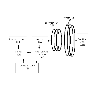
One approach for powering the prosthetic devices uses coupled coil
transmission --
this approach has been adopted by groups involved in the retinal prosthetics.
Referring to
Fig. 13a, the coil transmission assembly can include an AC magnetic field
generated by a
primary coil 122 on the outside of the eye 120, mounted, along with a coil
drive circuit 128,
on a pair of glasses that can be worn by the patient. Placement of the
secondary coil 124 can
be at the temporal side of the eye 120, as shown in Fig. 13b, to simplify
transmission. This
allows the coil and electronics to be attached to the sclera on the outside of
the eye, while
the electrodes of the nanowire array extend through a flap in the sclera to
the subretinal
space. Alternatively, the coil 124 could be placed against the retina, which
would be most
convenient since the coil, electronics and nanowire array could be implanted
as one package.
However, the fragility of the retina precludes placement of a thick or heavy
implant, thus
limiting the possible power that could be delivered. Placing the coil in the
anterior chamber
would allow more power to be delivered but is surgically difficult. Another
alternative is to
place the coil on the outside surface of the eye under the conjunctiva on the
front of the eye.
This location, or the location on the temporal side of the eye, allows the
greatest amount of
power to be delivered.
The design of secondary coil 124 will be limited by the maximum space around
the
eye and the heating due to the magnetic field (ANSI limit for field induced
power in a tissue
is 1781aW). The wireless circuit shown in Fig. 13a includes a rectifier 125 to
convert the AC
field induced by the primary coil 122 to DC for storage by battery 127. This
is a typical
design for inductive power delivery. However, because the nanowircs 130
require AC bias
to produce the biphasic currents needed for neural stimulation, an inverter
129 is included to
convert the DC back to AC. Control circuitry 132 is connected to battery 127
and inverter
129 for controlling operation of the nanowire array 130. This design, although
expected to
be robust, would consume excessive of power.
In an alternative embodiment, the rectifier and inverter are eliminated, and
the AC
induced field is used to directly power the nanowires. In this embodiment, it
may be
advantageous to change the site or size of secondary coil to improve alignment
with the
primary coil.
CA 02803319 2012-12-19
WO 2011/163262 PCT/US2011/041293
-18-
A nanowire-based device constructed according to the present invention will
carry a
scalable modality capable of dual function of light detection and neural
stimulation with
tunable performance.
Fig. 14 is a diagram of nanowire ridges 138 pattered over a silicon substrate.
In human
and primate retinas, a small central area of the macular region of the retina
called the 'fovea'
is specialized for high resolution vision and sensitivity to fine details. The
center of the
fovea, the foveola, has a high concentration of very compact cones and
virtually no rods.
The fovea plays a key role in visually guided behavior. It has been shown that
line-shaped
stimulation electrodes can lead to selective activation of local ganglion
cells, avoiding co-
.. stimulation of axons originating from ganglion cells of the outer regions
(Rattay, F.,
"Effective electrode configuration for selective stimulation with inner eye
prostheses", IEEE
Trans Bioined Eng., 2004 Sep;51(9):1659-64.) Nanowire ridges 138, on the order
of 541m -
4001,tm in length and having widths corresponding to the thickness of the
nanowires (50nm
to Iglu), can be formed using processes similar to those described above.
Photolithography
can then be used to pattern electrodes 140 in different shapes and sizes for
selective line
stimulation. Such stimulation sites would cover an area along the nanowires.
The ridges can
be tapered or have sharp edges.
The inventive nanowire platform can be used for recording action potentials
from
neurons extracellularly and intracellularly. The recording can be improved by
using any of
the following materials on the tips of the nanowires, including stainless
steel, tungsten,
platinum, platinum-iridium alloys, iridium oxide, titanium nitride, and
poly(ethylenedioxythiophene) (PEDOT). The deposited material can connect one
or a
bundle of nanowires to one lead, which is also made of the same material. A
basic
neuroamplifier circuit 154 can be used to condition and amplify the recorded
action
potential. This recording potential can be combined with the stimulation in an
implant. Fig.
15 provides an example of the nanowire platform can be used to record
extracellular or
intercellular potential from a neuron. The nanowires 150, with enhanced tips
148, may be
positioned near a neuron in a slice, animal or cell culture model (cell
membrane 152 is
shown). Basic circuitry, design of which will be readily apparent to those of
skill in the art,
CA 02803319 2012-12-19
WO 2011/163262 PCT/US2011/041293
-19-
will be included to condition and amplify the acquired signal. Display 156
illustrates an
example of the acquired signal. The resulting signal may be stored in a memory
device 158.
The nanowire platform of the present invention may be used as an interface and
potential prosthesis to generate a nanoscale molecular signaling cue or
stimulation based on
.. electric currents for the induction of chemically secreted neuroprotective
factors from cells,
i.e., not just neurons, but glial cells and other central and peripheral
nervous system cells.
In one example, nanowirc arrays may be engineered into a broader device to act
as
an electrical-to-chemical transducer in the development of a nanoengineered
artificial
chemical synapse. The nanowires may be configured to respond to light or some
other input
.. signal. In response to detection of such an input, the array may use its
electrical properties
to trigger the release of chemically-based signaling molecules, such as
various classes of
neurotransmitters (e.g., peptides or catecholamines) from a thin film,
polymer, or other
synthetically engineered material. In one example, a synthetic
neurotransmitter may
encapsulated within cells or layers in a membrane formed from an electroactive
polymer
into which the nanowire electrodes extend. The membrane, when activated, opens
the cells
(or pores in the layers) for a sufficient duration to release the appropriate
quantity of the
neurotransmitter to effect the desired change. The released molecules can then
chemically
stimulate and signal neurons, thus inducing or mimicking synaptic behaviors.
Nanowire-
based devices of this type may be useful for treatment of a wide range of
conditions
involving synaptic dysfunction or failure, including but not limited to,
depression,
Alzheimer's disease, Parkinson's disease, and may even be useful in treating
drug addiction
and some forms of paralysis.
In still another application of the inventive nanowire platform, individually
addressable nanowires, or bundled nanowires, as shown in Fig. 16, can be used
as an imager
.. array for a retinal prosthesis. In this application, the nanowires would
not be in contact with
the cells in the retina. Instead, a device with stimulating electrodes, in the
form of a
microelectrode array (MEA) 160 fabricated from a flexible material (PDMS,
PARYLENETM
or polyimide), may be placed in the subretina or epiretina and connected to
the nanoimager.
An inductive link, similar to that described above (not shown here), can be
used to power
the device. The flexible MEA 160 can have electrodes 152 with diameters
ranging from
CA 02803319 2012-12-19
WO 2011/163262 PCT/US2011/041293
-20-
100gm to lgm formed using materials including platinum, platinum-iridium
alloys, iridium
oxide, titanium nitride, and poly(ethylenedioxythiophene) (PEDOT).
Photocurrent produced
by the bundled or individually-addressable nanowires 164 can be sent into the
stimulation
electrodes 152. Additional circuitry 166 can be added to fine tune the output
of the
nanowires before it is sent to the MEA. The conditioning involves control over
waveform
shape, height and duration.
In addition to its application as a retinal prosthesis, the molecular scale of
the
inventive nanowire platform makes it broadly applicable as an interface and
potential
prosthesis for other sensory systems and non-sensory parts of the brain and
central nervous
system.
References (incorporated herein by reference.)
1) Kim, H., et al., "Fabrication of Vertical Silicon Nanowire Photodetector
Arrays using
Nanoimprint Lithography", Proceedings of SPIE, 2010, pp. 7591-7595.
2) Soci, C., et al., "ZnO Nanowire UV Photodetectors with High Internal Gain",
Nano
Letters, 2007, Vol. 7, p. 1003.
3) Zhang, A., et al., "Silicon Nanowire Detectors Showing Phototransistive
Gain", Applied
Physics Letters, 2008, Vol. 93, 121110-1-3.
4) Khraiche, M.L., N. Jackson, and J. Muthuswamy. Biology Society, 2009. EMBC
2009.
Annual International Conference of the IEEE, 2009.
5) Humayun, M.S., et al., "Visual perception in a blind subject with a chronic
microelectronic retinal prosthesis", Vision Res., 2003, 43(24), pp. 2573-2581.
6) Winter, JØ, et al., "Retinal prostheses: current challenges and future
outlook", Journal
of Bioinaterials Science, Polymer Edition, 2007, 18, pp. 1031-1055.
7) Besch, D., et al., "Extraocular surgery for implantation of an active
subretinal visual
prosthesis with external connections: feasibility and outcome in seven
patients ",. Br.
J. Ophthalmol, 2008, 92(10): p. 1361-8.
8) Zhang, A., et al., "Nanowire Photodetectors", Journal of Nanoscience and
Nanotechnology, 2010, 10: p. 1430-1449.
CA 02803319 2012-12-19
WO 2011/163262 PCT/US2011/041293
-21-
9) Zhang, A., et at., "Characterization and physics of top-down silicon
nanowire
phototransistors", Proceedings of SPIE, 2010, 7608, p. 76081D-8.
10) Sun, K., et al., "Compound Semiconductor Nanowire Solar Cells" Selected
Topics in
Quantum Electronics, IEEE Journal of, 2010. PP(99): p. 1-17.
.. 11) Soci, C., et al., Nanowire Photodetectors. Journal of Nanoscience and
Nanotechnology,
2010, 10(3): p. 1439-1449.
12) Curcio, C.A., et al., "Human photoreceptor topography", J Comp Neurol,
1990, 292(4):
p. 497-523.
13) Friedburg, C., M.M. Thomas, and T.D. Lamb, "Time course of the flash
response of
dark- and light-adapted human rod photoreceptors derived from the
electroretinogram", J Physiol, 2001. 534(Pt 1): p. 217-42.
14) Palanker, D., et al., "Design of a high-resolution optoelectronic retinal
prosthesis"õI
Neural Eng, 2005, 2(1): p. S105-20