Note: Descriptions are shown in the official language in which they were submitted.
CA 02803333 2012-12-20
WO 2011/161401 PCT/GB2011/000920
MAGNETRON POWER SUPPLY
The present invention relates to a power supply for a magnetron, in particular
but not exclusively for use with a magnetron powering a lamp.
It is known that magnetrons can change mode unexpected, that is to say that
unexpectedly they can stop oscillating at one frequency and start oscillating
at
another. Under these conditions, they can exhibit negative impedance. This can
result in damagingly high current flow. For this reason, it is known that
constant/controlled voltage power supplies are not suitable for magnetrons;
constant/controlled current power supplies are usually used for powering them.
Anode voltages in magnetrons are high and measurement of both anode
voltage and anode current are difficult.
In a previous power supply invented by the present inventor, measurement of
both voltage applied to a converter in a magnetron power supply and current
through
the converter was utilised in a conjunction with a microcomputer to provide
real time
control of power supplied to a magnetron. The microcomputer was programmed to
compute:
1. Power being consumed,
2. A difference from a desired power and
3. A difference between the power difference and the measured current.
This second difference signal was used to control the converter. It should be
noted
that these three steps were executed in software. Unexpectedly, this power
supply
still suffered from a degree of instability, causing perceivable flickering of
the light
produced by its magnetron powered lamp.
Experience has now shown that the eye is extremely sensitive to light flicker
in a magnetron powered plasma lamp. It has now been appreciated that the
limited
speed and resolution of the microprocessor output capability aggravated the
perceived
flickering. Additionally, two of the inputs to the microprocessor, namely the
voltage
applied to the converter and the current drawn through the converter are
liable to be
CA 02803333 2012-12-20
WO 2011/161401 PCT/GB2011/000920
2
noisy and multiplication of the two noisy signals is believed to have
contributed to the
instability.
Simply filtering of the noise from the microprocessor reduces unacceptably
the reaction time of the control circuit and contributes to instability,
bearing in mind
that fast reaction to changed magnetron conditions can be required.
Accordingly a
new approach was required.
The object of the present invention is to provide an improved power supply for
a magnetron.
According to the invention there is provided a power supply for a magnetron
comprising:
= a DC voltage source;
= a converter for raising the output voltage of the DC voltage source, the
converter having:
= a capacitative-inductive resonant circuit,
= a switching circuit adapted to drive the resonant circuit at a variable
frequency above the resonant frequency of the resonant circuit, the
variable frequency being controlled by a control signal input to provide an
alternating voltage,
= a transformer connected to the resonant circuit for raising the alternating
voltage,
= a rectifier for rectifying the raised alternating voltage to a raised DC
voltage for application to the magnetron;
= means for measuring the current from the DC voltage source passing through
the converter;
= a microprocessor programmed to produce a control signal indicative of a
desired output power of the magnetron; and
= an integrated circuit arranged in a feed back loop and adapted to apply a
control signal to the converter switching circuit in accordance with a
comparison of a signal from the current measuring means with the signal
CA 02803333 2012-12-20
WO 2011/161401 PCT/GB2011/000920
3
from the microprocessor for controlling the power of the magnetron to the
desired power.
Provision of the integrated circuit as a discrete element separate from the
microprocessor provides a fast control loop, which is not limited by the speed
of the
microprocessor. (The latter is liable to be slow due to economic constraints
on it
specification.) Thus the power supply of the invention is inherently more
stable and
provides less flicker-prone illumination.
Whilst it can be envisaged that the integrated circuit could be a digital
device,
in the interests of economy, it is preferably an analogue device. In the
preferred
embodiment, the integrated circuit is an operational amplifier.
In the preferred embodiment the operational amplifier is arranged as an
integrator with a feedback capacitor whereby its output voltage is adapted to
control a
voltage to frequency circuit for controlling the converter.
Preferably the microprocessor is programmed to filter noise from the desired
converter current signal. Alternatively a filter circuit can be provided
between the
microprocessor and the operational amplifier.
In the preferred embodiments, the switching circuit is adapted to control the
frequency of the converter in accordance with a variable voltage signal output
from
the operational amplifier. In this technique, an increase in frequency
corresponds to a
reduction in magnetron drive voltage and microwave output.
Alternatively the switching circuit can be adapted to control the duty cycle
of
the converter in accordance with the operational amplifier output, whereby
reduction
in the duty cycle corresponds to a reduction in magnetron drive voltage and
microwave output.
In the preferred embodiments, the converter is a zero voltage switching
device; although it could be a zero current switching device.
CA 02803333 2012-12-20
WO 2011/161401 PCT/GB2011/000920
4
Normally the switching circuit will have its own oscillator; however, it can
be
envisaged that it could be timed from a clock in the microprocessor.
In one embodiment, the integrated circuit is adapted and arranged for the
comparison to be direct between the measured current signal and the desired
power
signal, the integrated circuit being connected to receive these signals only,
whereby
the converter current is controlled in accordance with the desired power
independent
of transient changes in the voltage of the DC voltage source. This embodiment
controls the average power to be constant over voltage source ripple cycles.
In another embodiment, the integrated circuit is adapted and arranged for the
comparison to be not only between the measured current signal and the desired
power
signal but also taking account of transient changes in the voltage of the DC
voltage
source, a signal indicative of the voltage of the voltage source also being
input to the
integrated circuit, whereby the converter current is controlled such that the
power
passing through the converter is controlled in accordance with the desired
power. This
embodiment controls the instantaneous power constant to be constant through
voltage
source ripple cycles.
Normally the switching circuit will have its own oscillator; however, it can
be
envisaged that it could be timed from a clock in the microprocessor.
To help understanding of the invention, a specific embodiment thereof will
now be described by way of example and with reference to the accompanying
drawings, in which:
Figure 1 is a block diagram of a pri or power supply for a magnetron;
Figure 2 is a similar block diagram of a power supply in accordance with the
invention;
Figure 3 is a more detailed circuit diagram of the power supply of Figure 2;
Figure 4 is a diagrammatic view of a lamp powered by a magnetron having a
power supply of the invention;
Figure 5 is a circuit diagram of a second embodiment of the invention;
Figure 6 is details of the voltage divider of the embodiment of Figure 5;
CA 02803333 2012-12-20
WO 2011/161401 PCT/GB2011/000920
Figure 7 is a spectral diagram of in agnetron output comparing that of the
embodiments of Figure 3 and 5; and
Figure 8 is a circuit diagram of a third embodiment of the invention.
5 Referring first to Figure 1, there is shown diagrammatically a prior power
supply having an oscillator 1 connected to power a magnetron 2 and controlled
by a
microprocessor 3. An augmented mains voltage, DC voltage source 4 supplies
typically 400 volts on line 5 to the oscillator 1. This feeds alternating
current to a
transformer 6 and rectifier 7 from which 4000 DC volts is applied on line 8 to
the
magnetron. The oscillator, transformer and rectifier are referred to as a
"high voltage
converter". Power being supplied to the magnetron is measured in terms of the
voltage across a resistor 9 in the earth return of the converter. The voltage
is
indicative of the current in the resistor 9 and is proportional to the power
applied to
the magnetron, assuming constant voltage from the voltage source 4. The
resistor
voltage is one input on line 10 to the microprocessor. Another input on line
11
applies the voltage on line 5 to the microprocessor. A desired power control
value 12
is set externally or as a manual input to microprocessor.
The microprocessor is programmed to perform the steps of :
1. Multiplication of the voltage on line 5 with current in resistor 9 to
compute the
power being supplied to the magnetron, assuming high efficiency;
2. Comparison of the computation of the power being consumed with the desired
power and thence a computation of the current that should be being consumed
(the intended current);
3. Comparison of the intended current with the measured current and
application to
the power supply of an incrementally higher voltage to drive the converter at
a
higher frequency if the current is high or any incrementally lower voltage if
the
current is to low. It should be noted that if the converter operates at a
higher
frequency, the resultant voltage across the magnetron drops.
As already mentioned, this circuit proved in use to be too unstable for
flicker
free operation of the magnetron as a light source.
CA 02803333 2012-12-20
WO 2011/161401 PCT/GB2011/000920
6
Turning now to Figure 2, a power supply of the invention comprises the
following similar components connected in the same manner:
= oscillator / high voltage converter 101;
= magnetron 102;
= transformer 106
= rectifier 107
= resistor 109.
A microprocessor 103 is also included, but it operates quite differently. It
1o merely divides a desired power control value 112 by the augmented mains DC
voltage
on the line 105, and provides a required current signal on line 121 indicative
of the
desired current through the converter 101 to operate the magnetron at the
desired
power. The signal on line 121 is fed to one input of an operational amplifier
122/EA1. Its other input has a line 110 to it from the resistor 109,
indicating the
actual current passing through the converter. The operational amplifier is
connected
as an integrating error signal magnifier.
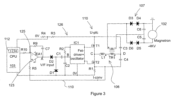
Turning on now to Figure 3 there is shown a fuller circuit diagram of the
power supply of Figure 2. Central to it is a quasi-resonant oscillator 101 of
a high
voltage converter, having MOSFET field effect switching transistors Tl,T2.
These
are switched in a manner to be described below by an integrated circuit
oscillator IC 1.
An inductance L1 and primary coil of the transformer 106 are connected in
series to
the common point of the transistors T1,T2. Capacitors C3,C4 complete the
series
resonant circuit. The inductances and the capacitors determine a resonant
frequency,
above which the converter is operated, typically around 70kHz, whereby it
appears to
be primarily an inductive circuit as regards the down-stream magnetron
circuit. This
comprises four half bridge diodes D3,D4,D5,D6 and smoothing capacitors C5,C6,
connected to the secondary winding of the transformer and providing DC current
to
the magnetron 102. The windings ratio of the transformer is 10:1, whereby
voltage of
the order of 4000 volts is applied to the magnetron, the augmented mains DC
voltage
on line 105 typically being 400 volts.
CA 02803333 2012-12-20
WO 2011/161401 PCT/GB2011/000920
7
A feature of the converter circuit is that when the transistors TI,T2 are
switched ON and then OFF sequentially in turn, the energy stored in the
inductance
L1 inverts the voltage across it. This drives down the voltage at the common
point C
before TR2 switches on and drives up the common point voltage before TR1
switches
on. Thus switching occurs at zero or close to zero volts across the transistor
about to
be switched on, that is in ZVS mode (Zero-Voltage-Switching mode). This
contributes to reliability and longevity.
At high switching frequency (i.e. above resonance), the voltage at the common
1o point between the capacitors C3,C4 is substantially constant at half the
voltage on line
105, whereby on transistor switching, a substantially triangular wave form
ramp
current flows through the inductance L1. This is passed to the transformer and
thence
ultimately to the magnetron.
Lowering the frequency to operation closer to resonance increases the voltage
swing at D away from half the voltage on line 105 and increases the voltage at
the
magnetron, its current and its microwave output.
The current through the converter is measured at resistor 109/R1, typically
100mf , and a voltage indicative of it is passed via feed-back resistor R5,
typically
47052, to one input 123 of the operational amplifier 122. The microprocessor
103, via
a voltage divider R3,R4, receives the voltage from the line 105. A required
power
setting is set via a manual input 112. The microprocessor is programmed to
divide the
required power by the line voltage and apply to the other input 125 of the
operational
amplifier a voltage indicative of the converter current required for the
required
magnetron, via a 6kQ resistor R10. The operational amplifier has an
integrating
capacitor C7, typically 470nF in series with a resistor R9 IMS2. The ratio of
the
resistors R9,R10 determines the gain of the operational amplifier. This again
set to
suppress mains voltage flicker as much as feasible. The amplifier passes an
integrated
voltage indicative of the required power to a frequency control circuit 126
for the
oscillator ICI, which is a voltage to frequency circuit, typically Texas
Instruments
IRS2153 or ST Thomson L6569. The circuit comprising resistor R2 18kQ,
capacitors
C1,C2, both 470pF, and diodes D1,D2 operates to control the frequency of the
CA 02803333 2012-12-20
WO 2011/161401 PCT/GB2011/000920
8
converter. When the operational amplifier's output is zero, the capacitor Cl
is in
parallel with C2 and the lowest frequency is obtained. This corresponds to
maximum
magnetron power. On the other hand, when the output is maximum the diodes
never
conduct and the frequency is controlled by C2 alone. Maximum frequency and
minimum power - of the order of one tenth of the maximum - is supplied. At
intermediate voltages, Cl has an intermediate effect and the frequency and
power is
controlled accordingly.
Thus the magnetron can be controlled to operate at the desired power input to
the microprocessor. The microprocessor is susceptible to flicker inducing
variations
in the voltage on line 105. However, the signal to RIO can be filtered
internally by
software or externally by a non-shown RC filter. Should the magnetron power
consumption shift, as it can do as its magnets heat up and its resistance
changes, the
operational amplifier reacts fast to the change in current measured at the
resistor R1
and adjusts the frequency of the converter and hence corrects the power
consumption
by the magnetron independently of the signal on line 125 from the
microprocessor.
That said, if there is flicker on the voltage source line, the power of the
magnetron will be constant only when averaged over the flicker period. There
does
tend to be double mains frequency flicker on the voltage source line, due to
the cost of
large smoothing capacitors.
It should be noted that the above described power supply is particularly
suited
to control of the LER magnetron powered lamp as described in WO 2009/063205.
It
enables the light output of the lamp to be controlled at will as and when
required from
low level for background light to full power full illumination.
Shown in Figure 4 is a simplified representation of a lamp driven by the
magnetron. It has a lucent crucible 201 with a Faraday cage 202. A void 203 in
the
crucible has a fill 204 of excitable material. The magnetron 205is arranged to
project
its microwaves into a waveguide / transition 206 from which they exit on a
coaxial
connection 207 to an antenna 208 releasing them into the crucible. Powering of
the
magnetron by a power supply 209 of the invention causes the excitable material
to
CA 02803333 2012-12-20
WO 2011/161401 PCT/GB2011/000920
9
emit light. It is this light that the power supply of the invention is
advantageous for in
avoiding flickering.
Turning now to Figure 5, there is shown an improved high voltage converter,
also in accordance with the invention. It takes account not only of variations
in the
converter current, and hence the magnetron current, but also mains frequency
ripple -
or more precisely twice main frequency ripple on the output of the voltage
source.
This ripple does not cause perceptible flicker in the light from the LER, but
does
induce bandwidth spreading in the output of the magnetron.
The modification of Figure 5 is the inclusion of a resistor R6, in the form of
two IMO resistors in series, from the voltage source line to the operational
amplifier
input 123 to which the feed back resistor R5 is connected. The resistors R6-R5
form
a voltage divider. The divider is such that the voltage across the resistor R5
is
substantially the same as the voltage across the current measuring resistor,
typically
both of the order of 100mV, giving 200mV at the operational amplifier input.
The
actual voltage varies with both the actual current in the converter and the
actual
voltage on the voltage source line. It will be appreciated that an increase in
the
operational amplifier input of 200mV due to increase in the voltage source
line will be
equivalent to an increase in the operational amplifier input 200mV due to
increase in
the current. Both raise the integrated output voltage of the operational
amplifier, with
the result that the controlled current is reduced.
The actual increase in operational amplifier input due to a 5% increase in the
voltage source voltage will be 5%, because the voltage across the current
measuring
resistor is small compared to the voltage source voltage. Equally for a 5%
increase in
current, the voltage across the current measuring resistor will be 5%. This
will be
added to the voltage at the operational amplifier input. Thus for a 5% or
other small
percentage increase in the voltage or the current, the current will be reduced
by the
same percentage.
In turn this results in a 5% or other small percentage reduction in the power
being applied to the magnetron. Thus the arrangement acts to keep
instantaneous
CA 02803333 2012-12-20
WO 2011/161401 PCT/GB2011/000920
power constant. In this respect, instantaneous is used to mean that the power
is kept
constant throughout the cycle of the voltage ripples for instance.
This operation can be explained mathematically as follows:
5
The power of the magnetron is the product of the voltage source voltage U and
the converter current I, i.e.
P=UxI.
In terms of units of voltage and current, u and I:
10 P = (Clx u) x (C2x i)
P=Kx(uxi)
With u and i having unit value, this formula can be rewritten as
P=Kx(u+i)/2.
This relationship remains approximately correct for small variations in
voltage and
current, i.e. for u Su, i 8i.
The above equation can be rewritten as
P=K3+K4x8V+K5x8v.
Thus the power of the magnetron can be represented as a constant plus another
constant times any deviation of the actual voltage source from its nominal
value plus
another constant times any deviation of the current from a nominal current.
The
current deviation itself can be represented of the voltage across the current
measuring
resistor.
With appropriate constants, and considering only the variations input to the
operational amplifier, it can be seen that the voltage divider does input the
sum of the
two variations in voltage source voltage and converter current to the
operational
amplifier. The only proviso is that the approximation
P=UxI~ Kx(u+i)/2
Is satisfied only if the voltage across R5 is approximately equal to that
across RI.
This is satisfied for the values:
U = 400volts
CA 02803333 2012-12-20
WO 2011/161401 PCT/GB2011/000920
11
RI = 0.1Q
R5 = 470Q
R6 = 2MS2.
These resistors are shown in series in Figure 6, with indication of the
relevant
voltages also shown.
It should be noted that because R6 is seven orders of magnitude greater than
R1 and R5 is four orders of magnitude greater, any change in U which create an
1o appreciable change of voltage at the operational amplifier input is
unlikely to cause an
appreciable change of voltage across R1, whose voltage is controlled only by
the
current through it. Accordingly the voltage across R1 is added to that across
R5 and
the sum is input to the operational amplifier.
It will be appreciated that this means of operation is not exactly linear, but
it
does provide significant improvements. With reference to Figure 7, there is
shown a
saddle shaped graph of the bandwidth of frequency of the magnetron's
generation. Its
generation frequency is dependent on the current through it, it being a
feature of a
magnetron that it has a characteristic akin to that of a zener diode in
controlling the
voltage across it. Thus if more power is available to it, its current
increases and with
its operating frequency is lowered. Where there is a mains voltage related
ripple on
the voltage of the voltage source, the magnetrons frequency varies and the
bandwidth
exhibits a slight saddle shape. By contrast, with the power control of the
embodiment
of Figure 5, the bandwidth is much narrower and has a Gaussian distribution.
This in
its turn is advantageous in causing much less interference with Bluetooth
communication networks and the like
Turning on to Figure 8, a multiplier circuit 301 is shown at the input to the
operational amplifier. This circuit is an analogue device, although a digital
device is
conceivable, and has the mid-point of the common point of the R6-R7 potential
divider applied to one input and voltage signal from the current measuring
resistor R1
applied to the other input. The multiplier multiplies these two voltage and
current
indicating signals together to produced and apply to the input of the
operational
amplifier a signal indicative of the magnetron power. This embodiment is more
CA 02803333 2012-12-20
WO 2011/161401 PCT/GB2011/000920
12
precise than that of Figure 5, but is more expensive in that multiplier
circuits are little
used and tend to be expensive. We regard the embodiment of Figure 5 as being
better
in that it is adequately accurate and at the same time is cheaper.