Note: Descriptions are shown in the official language in which they were submitted.
CA 02803586 2012-12-20
WO 2012/004557 PCT/GB2011/001015
MICROWAVE DRIVEN PLASMA LIGHT SOURCE
The present invention relates to a plasma light source.
In European Patent No EP1307899, granted in our name there is claimed a
light source comprising a waveguide configured to be connected to an energy
source
and for receiving electromagnetic energy, and a bulb coupled to the waveguide
and
containing a gas-fill that emits light when receiving the electromagnetic
energy from
the waveguide, characterised in that:
(a) the waveguide comprises a body consisting essentially of a dielectric
material
having a dielectric constant greater than 2, a loss tangent less than 0.01,
and a DC
breakdown threshold greater than 200 kilovolts/inch, 1 inch being 2.54cm,
(b) the wave guide is of a size and shape capable of supporting at least one
electric
field maximum within the wave guide body at at least one operating frequency
within the range of 0.5 to 30GHz,
(c) a cavity depends from a first side of the waveguide,
(d) the bulb is positioned in the cavity at a location where there is an
electric field
maximum during operation, the gas-fill forming a light emitting plasma when
receiving microwave energy from the resonating waveguide body, and
(e) a microwave feed positioned within the waveguide body is adapted to
receive
microwave energy from the energy source and is in intimate contact with the
waveguide body.
In our European Patent No 2,188,829 there is described and claimed a light
source to be powered by microwave energy, the source having:
= a body having a sealed void therein,
= a microwave-enclosing Faraday cage surrounding the body,
= the body within the Faraday cage being a resonant waveguide,
= a fill in the void of material excitable by microwave energy to form a light
emitting plasma therein, and
= an antenna arranged within the body for transmitting plasma-inducing,
microwave energy to the fill, the antenna having:
CA 02803586 2012-12-20
WO 2012/004557 PCT/GB2011/001015
2
= a connection extending outside the body for coupling to a source of
microwave energy;
wherein:
= the body is a solid plasma crucible of material which is lucent for exit of
light
therefrom, and
= the Faraday cage is at least partially light transmitting for light exit
from the
plasma crucible,
the arrangement being such that light from a plasma in the void can pass
through the
plasma crucible and radiate from it via the cage.
We refer to this as our Light Emitting Resonator or LER patent. Its main
claim as immediately above is based, as regards its prior art portion, on the
disclosure
of our EP 1307899, first above.
In our European Patent Application No 08875663.0, published under No
W02010055275, there is described and claimed a light source comprising:
= a lucent waveguide of solid dielectric material having:
= an at least partially light transmitting Faraday cage surrounding the
waveguide, the Faraday cage being adapted for light transmission radially,
= a bulb cavity within the waveguide and the Faraday cage and
= an antenna re-entrant within the waveguide and the Faraday cage and
= a bulb having a microwave excitable fill, the bulb being received in the
bulb
cavity.
We refer to this as our Clam Shell application, in that the lucent wave guide
forms a clam shell around the bulb.
As used in our LER patent, our Clam Shell application and this specification:
= "microwave" is not intended to refer to a precise frequency range. We use
"microwave" to mean the three order of magnitude range from around 300MHz to
around 300GHz;
= "lucent" means that the material, of which an item described as lucent is
comprised, is transparent or translucent;
CA 02803586 2012-12-20
WO 2012/004557 PCT/GB2011/001015
3
= "plasma crucible" means a closed body enclosing a plasma, the latter being
in the
void when the void's fill is excited by microwave energy from the antenna;
= "Faraday cage" means an electrically conductive enclosure of electromagnetic
radiation, which is at least substantially impermeable to electromagnetic
waves at
the operating, i.e. microwave, frequencies.
We have recently disclosed LER improvements in Patent Applications filed on
30th June 2011, under Nigel Brooks references Nos 3133 and 3134. The
improvements relate to the incorporation of a lucent tubes within a bore in
the solid
body, the tube being integral with the body and having the void formed in it.
In order
to put beyond doubt that the present improvement applies to the improvements
of
these two applications, we define as follows:
The LER patent, the Clam Shell Applications and the above LER
improvement applications have in common that they are in respect of-
A microwave plasma light source having:
= a Faraday cage:
= delimiting a waveguide and
= being at least partially lucent, and normally at least partially
transparent,
for light emission from it, and
= normally having a non-lucent closure;
= a body of solid-dielectric, lucent material embodying the waveguide within
the
Faraday cage;
= a closed void in the waveguide containing microwave excitable material; and
= provision for introducing plasma exciting microwaves into the waveguide;
the arrangement being such that on introduction of microwaves of a determined
frequency a plasma is established in the void and light is emitted via the
Faraday cage.
In this specification, we refer to such a light source as a Lucent Waveguide
Microwave Plasma Light Source or LWMPLS.
CA 02803586 2012-12-20
WO 2012/004557 PCT/GB2011/001015
4
With the objective of improving our LWMPLS, we have determined that by
comparison with conventional plasma lamps using electroded bulbs we can
achieve
higher wattage per unit length of plasma.
To set this in perspective, the light output and lives of conventional
electroded
plasma, i.e. HID (High Intensity Discharge), bulbs is very dependent on both
the
minimum and maximum wall temperature. The minimum wall temperature sets the
vapour pressure of the additives, the higher the additive pressure generally
the higher
the light output. The maximum wall temperature sets a limit on the life of the
bulb.
1o Below 725 C bulbs can have a long life; above 850 C the life deteriorates
rapidly.
The wall loading of a bulb is its input power divided by internal bulb surface
area, usually expressed in Watts per cm2. Wall loading is used as crude metric
to
encompass both temperatures. Many proposals have been made to minimise the
difference between these two temperatures. For long life of electroded bulbs,
greater
than 15,000hrs life, 20 Watts per cm2 is regarded as an upper limit while 50
Watts per
cm2 bulb lives are reckoned to be less than 2,000hrs.
The efficiency with which microwave energy is converted into light - in terms
of lumens per watt - increases in our LWMPLSs with their operating wattage,
all
other things being equal. This results from maximum temperature in the plasma
increasing and is linked to conductivity or skin depth of the plasma which
decreases
as the power per unit length is increased.
We have been surprised by how marked this effect is and accordingly, we now
believe that we can specify improved LWMPLS and LER performance, in terms of
them or at least their plasma voids being short for their operational power.
According to the invention there is provided a Lucent Waveguide Microwave
Plasma Light Source having a void length L and a rated power P, wherein:
= the plasma loading of the rated power divided by the void length, i.e. P/L,
is at
least 100W per cm,
CA 02803586 2012-12-20
WO 2012/004557 PCT/GB2011/001015
the void length being the overall void length minus two radii of a central
portion of
the void.
We prefer to operate at 125W per cm or higher and for higher powers at least
5 140W per cm.
Measuring plasma loading in terms of the actual length of the plasma in the
void, which may be able to be observed through the lucent waveguide, is
awkward.
We prefer to measure the overall length of the void and subtract its radius
from each
end on the basis that the plasma is strongest in the central parallel portion
of a domed
end void and does not extend to the extreme end of flatter ended voids. While,
it is
possible to measure the actual microwave power, or at least the power
transferred to a
magnetron powering a LWMPLS, we prefer to measure power in terms of the rated
power of the light source, i.e. the overall power consumption of the light
source.
In some of our LWMPLSs, the plasma void is directly in the lucent crucible,
as in our LER, and in others the plasma void is in a lucent bulb within a
lucent
waveguide as in our Clamshell Application. This invention and the definition
of our
LWMPLSs is not restricted to these two arrangements. Other arrangements are
the
subject of certain of our pending and un-published patent applications.
Again in certain of our LWMPLSs, we are able to operate at much lower
internal surface areas of their voids for their operational power.
In particular, we prefer to operate at a wall loading of between 100 W per cm2
and 300 W per cm2. For higher powers, we would normally expect to operate at
least
at 125 W per cm2 and preferably in the range between 150 W per cm2 and 250 W
per
cm2.
We measure wall loading in terms of the internal surface area of the part of
the
void for which we measure plasma loading, with the power being the rated
power.
CA 02803586 2012-12-20
WO 2012/004557 PCT/GB2011/001015
6
We ascribe the fact that we can operate at such higher wall loading than
traditionally to the conductive and radiant heat transfer occurring from our
lucent
crucibles and waveguides.
To help understanding of the invention, a specific embodiment thereof will
now be described by way of example and with reference to the accompanying
drawings, in which:
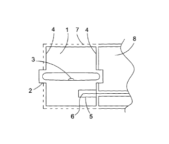
Figure 1 is a side view of an LER in accordance with the invention and
Figure 2 is a larger scale scrap view of the void.
Referring to the drawings, a lucent crucible 1 for an LER LWMPLS has a
central void 2 having microwave excitable material 3 within it. The void is
4mm in
diameter and 21mm long. The crucible is of fused quartz and is 21mm long
between
end flats 4 and is circular cylindrical with a 49mm outside diameter. The
identicalness of the length of the void and the length between the end flats
of the
crucible results from this being constructed from a piece of quartz, having a
bore and
closed at the ends of the bore. The length of the crucible - but not the void -
is
somewhat arbitrary for present purposes, because in the preferred TM010 mode,
resonance is independent of the crucible length. This LER is designed to
operate at
280 watts at 2.45GHz.
Also shown are a bore 5 for an antenna 6 to introduce microwaves into the
crucible and a Faraday cage 7 for retaining microwave resonance within the
crucible.
It is backed by an aluminium carrier 8 to which it is held by the cage.
With the LER operating at 280 Watts in TMp10 mode, corresponding to a
plasma loading of 133W per cm and a wall loading of 106W per cm2, we measure a
wall temperature of 700 C. Such a device has an efficacy of up to 110 lumens
per
Watt.
To measure the plasma loading, we divide the rated power of the LER by the
length of the plasma. In our experience the plasma 11 stops just short of the
full
length 12 of the void, as shown in Figure 2. The void generally has domed ends
14.
= Printed: 10-10-2012: DESCPAMD PCT/GB 2011/001 015
03/ 10 2012 14:46 FAX 01730823580 CA 02803586 2012-12-20 EPD MUNICH [A 007/010
PCT/GB 2011/001 015 - 03-10-201-
7
We measure the overall length of the void and subtract its radius 15 from each
end on
the basis that the plasma is strongest in the central parallel portion of a
domed end
void and does not extend to the extreme ends of flatter ended voids.
In order to achieve efficacies > 110lumens per Watt we have found it
necessary to increase the loading per unit length of plasma to be greater than
150 W
per cm. In order that the lamp has a reasonable lifetime, simultaneously, we
have
found it necessary to restrict the maximum wall loading to be less than 300 W
per cm2
and preferably less than 250 W per cm2.
Examples of higher plasma loadings for crucibles operating in the TM0j0 mode
are:
1. Void Length 11 mm
Void Diameter 5mm
Power 280W
Plasma Loading 255W per cm
Wall Loading 162W per cm2
2. Void Length 14mm
Void Diameter 3mm
Power 280W
Plasma Loading 200W per cm
Wall Loading 210W per cm2
Thus for high efficiency LERs with reasonably long life the operating
conditions may be set out as follows:
Arc or plasma loading Power input per unit length of plasma > 100 W per cm
Wall loading 100 W per cm2 < Plasma crucible wall loading < 300W
per cm2
Preferred wall loading 100 W per cm < Plasma crucible wall loading < 250W
I per cm2
->n: 03.10.2012 15:52:38 - 03.10.2012 15:54:07. This page 7 of 1 AM EN D ED S
H EET012 15:53:51
ceived at the EPO on Oct 03, 2012 15:54:07. Page 7 of 10
/1' 03-10-2012
CA 02803586 2012-12-20
WO 2012/004557 PCT/GB2011/001015
8
While these conditions apply to resonators operating in any mode, cylindrical
LERs operating in the TMO 10 and TM 110 modes have advantages in ease of
manufacturability and cost compared to resonators operating in other modes.
This is
because these two modes have the property that the resonant frequency is
independent
of the length of the cavity. This makes it particularly easy to vary the power
input per
unit length of plasma by varying the length of the LER and using butt sealed
tubes at
each end of the resonator the cost is kept to a minimum.