Note: Descriptions are shown in the official language in which they were submitted.
CA 02803772 2016-10-17
- 1 -
METHODS OF FORMING GRAPHENE BY GRAPHITE EXFOLIATION
FIELD
[0001] The present disclosure relates to methods of forming graphene, and in
particular relates to methods of forming graphene by exfoliation of graphite.
BACKGROUND ART
[0002] Graphene (G) is a two dimensional sheet of atomic carbon with very
attractive physical, optical and mechanical properties, including high charge
carrier
mobility, record thermal conductivity and stiffness.
[0003] Currently, upwardly scalable graphene synthesis methods mainly include
a
solution-based graphite oxide-mediated route and chemical vapor deposition
(CVD).
[0004] Graphite oxide-derived methods of forming graphene produce graphene
samples with poor crystalline quality and high defect density. Films prepared
by
such methods required a high-temperature annealing process to convert the
graphene from an insulator to a conductor. The CVD method is suitable for
preparing large-area thin films, but is not amenable to solution-based
processing.
Solution-based processing is needed for bulk processing of graphene
composites,
blends, inks, etc.
[0005] Conventional methods for the solution-based synthesis of graphene from
direct exfoliation/intercalation have yields that are generally less than 10%.
This
means 90% of the starting material, which is graphite, remained unexfoliated,
and
only 10% or less of the starting material is recovered as graphene flakes,
each
comprising one or a few layers of graphene. A problem with such low-yield
methods
is that they require multiple steps to generate sufficient products for
further
CA 02803772 2012-12-21
WO 2011/162727
PCT/SG2011/000225
- 2 -
processing, and include tedious multiple steps of separating the unexfoliated
materials from the exfoliated material.
[0006] Thus, there is a need for a high-yield method of forming graphene
flakes
directly from graphite that bypasses oxidation treatment, i.e., without
forming
graphene-oxide (GO).
SUMMARY
[0007] This disclosure describes a high yield (e.g., 90%) method of directly
exfoliating graphite into "few-layer" (i.e., one or more layers of) graphene
(sp2
carbon) without going through an oxidation route (i.e., without forming sp3
carbon,
such as graphene oxide). A distinguishing feature of the method described
herein is
that it does not use oxidizers like nitric acid (HNO3) or sulfuric acid
(H2SO4) as
reagents.
[0008] The exfoliated graphene produced by the methods described herein can be
dispersed in solutions and recovered readily from the insoluble parent
compound,
graphite. These exfoliated graphene flakes can be functionalized by various
organic
and inorganic components. The high-yield method allows for bulk synthesis of
high-
quality graphene in large quantities for industrial-scale processing of
polymer blends,
composites, capacitors, lithium storage, DNA extraction, biosensors, solar
cells,
conductive paper, as well as conductive, transparent sheets.
[0009] An aspect of the disclosure involves using the graphene created by the
methods disclosed herein to fabricate a nanocrystal/graphene heterojunction
solar
cell, which can be made to have record power conversion efficiency (e.g.,
3.2%).
Graphene solutions suitable for spin casting, roll-to-roll, ink-jet printing
or other
solution-based techniques are also disclosed that facilitate fabrication of a
wide
variety of graphene-based devices. The solution-based device fabrication
process is
low cost, scalable and has low toxicity. Use of the graphene as formed herein
in
solar cells and high sensitivity bio-extraction and detection, as well as in
forming
conducting sheets that are opaque (e.g., from paper) or transparent (e.g.,
from
plastic) are also described.
CA 02803772 2012-12-21
WO 2011/162727
PCT/SG2011/000225
- 3 -
[0010] An aspect of the disclosure is a high-yield, oxidation-free method of
exfoliating graphite into one or more layers of graphene, e.g., "few-layer
graphene."
The method can serve as a bulk processing route for high quality, conducting
graphene that is scalable for industrial production. Compared to oxide-derived
graphene, the graphene flakes produced by the present methods have fewer
defects
and are more conducting and more hydrophobic, making the graphene flakes more
suitable for solar cells and other applications as compared to graphene flakes
formed
via an oxidation process.
[0011] The foregoing general description and the following detailed
description
present embodiments of the disclosure, and are intended to provide an overview
or
framework for understanding the nature and character of the disclosure as it
is
claimed. The accompanying drawings are included to provide a further
understanding of the disclosure, and are incorporated into and constitute a
part of
this specification. The drawings illustrate various embodiments of the
disclosure and
together with the description serve to explain the principles and operations
of the
disclosure. The claims as set forth below are incorporated into and constitute
part of
this specification.
BRIEF DESCRIPTION OF THE DRAWINGS
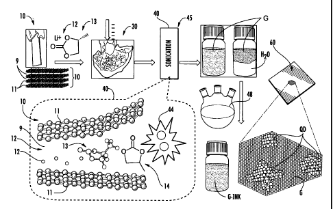
[0012] FIG. la is a schematic overview of the graphite exfoliation process to
form
few-layer graphene G, and also illustrates the fabrication of
nanocrystal/graphene
heterojunction that can be used as an active layer in solar cells;
[0013] FIG. lb is a schematic diagram of a general graphene-based
heterojunction;
[0014] FIGS. 2a-2b are SEM images and FIG. 2c is an atomic-force microscope
(AFM)
image of few-layer graphene G as exfoliated from graphite using the methods
described herein;
[0015] FIG. 2d are plots of the Raman spectra (514 nm laser) of a few layers
of
graphene G on Si substrates as compared to graphite;
[0016] FIGS. 3a-3g are electron microscopy images of nanocrystals/graphene
heterojunctions;
CA 02803772 2012-12-21
WO 2011/162727
PCT/SG2011/000225
- 4 -
[0017] FIGS. 4a-4c are plots illustrating the optical and optoelectronic
performances
of an example of quantum dots/graphene active layer in examples of thin film
solar
cell (i.e., photovoltaic or "PV") devices;
[0018] FIGS. 5a is a SEM image of graphene G as formed using the methods
described herein;
[0019] FIG. 5b shows two photographs, the left photograph being of pristine G
sheets floating on water and the right photograph being of G-ssDNA after
interaction
with single-stranded DNA (ss-DNA);
[0020] FIGS. Sc and 5d are plots of adsorbed material (mg/g) vs. concentration
of
material ( M) for ssDNA (FIG. Sc) and protein HCC (FIG. 5d) for both graphene
G and
graphene oxide GO;
[0021] FIG. 6a and 6b plot the circular dichroism (CD) spectra of free ssDNA
and G-
ssDNA (FIG. 6a) and native HCC, HCC adsorbed on graphene G and graphene oxide
GO (FIG. 6b);
[0022] FIG. 6c schematically illustrates how graphene G is used as a G-ssDNA
SELDI
probe;
[0023] FIG. 6d plots a SELDI-TOF MS spectra acquired directly after extraction
of 1:5
ssDNA & protein mixture (top) and after washing with DI water (bottom);
[0024] FIG. 6e plots the MS spectra of the BP parent ion and fragmented ion
using
graphene G (top) and graphene oxide GO (bottom) as a SELDI probe, with the
laser
fluence set at 40 mJ=cm-2;
[0025] FIG. 6f plots the MS spectra of HCC using a SELDI probe based on
graphene G
(top) and graphene oxide GO (bottom);
[0026] FIG. 7a through 7d illustrate various properties of flaked graphene
(FIG)
powder and its derived ink (G-INK) that can be used to make highly conductive
paper;
CA 02803772 2012-12-21
WO 2011/162727
PCT/SG2011/000225
-.5 -
[0027] FIG. 7e plots the paper resistance in (ohms per square) vs. the amount
of
graphene loading (mg/cm2) for sheets of paper coated with different amounts of
graphene ink;
[0028] FIG. 8a and FIG. 8d illustrate the formation of an example transparent,
conducting substrates (sheets) using highly continuous FIG films on plastic
substrates by manual polishing dried FLG powder;
[0029] FIG. 8c plots the transmittance (%) vs. wavelength (nm) for four
example
transparent, conducting sheets;
[0030] FIG 8d plots the resistance (kohms per square) vs. transparency (%) for
the
four example transparent, conducting sheets, with no annealing;
[0031] FIG.9a through FIG. 9e are electron microscopy characterizations of
asymmetric nanocrystal/graphene heterojunction of CdTe/graphene/PbS-Ti02;
[0032] FIG. 9f and FIG. 9g are electron diffraction patterns of an example
CdTe/graphene/PbS-Ti02 sheet;
[0033] FIG. 9h plots the results of an EDX analysis of the CdTe/graphene/PbS-
Ti02
sheet; and
[0034] FIG. 9i plots the concentration-dependent optical absorption spectra
(absorbance vs. wavelength) of the CdTe/graphene/PbS-Ti02 sheet of Fig. 9h as
dispersed in iso-propanol, with the "graphene only" dispersion shown for the
sake of
comparison.
[0035] The various elements depicted in the drawing are merely
representational
and are not necessarily drawn to scale. Certain sections thereof may be
exaggerated, while others may be minimized. The drawings are intended to
illustrate example embodiments of the disclosure that can be understood and
appropriately carried out by those of ordinary skill in the art.
DETAILED DESCRIPTION
[0036] Aspects of the present disclosure are directed to methods of forming
graphene G from graphite without forming graphene oxide. The method can be
CA 02803772 2012-12-21
WO 2011/162727
PCT/SG2011/000225
- 6 -
carried out in a manner that is highly efficient, e.g., 90%. Aspects of the
disclosure
also include multiple uses and applications of the graphene G produced using
the
methods described herein in areas such as biotechnology and solar cells. In
the
discussion below, graphene G is sometimes referred to G, graphene flakes
referred
to as FLG, and graphene oxide as GO where appropriate.
[0037] FIG. la is a schematic illustration of the method steps associated with
forming few-layer graphene G by exfoliating graphite 10, and also shows the
general
fabrication steps associated with forming nanocrystal/graphene heterojunction
solar
cells.
[0038] In a first step of an example of the graphene-forming method, an
initial
(starting) graphite sample (material) 10 is provided. In a second step, the
graphite
sample is intercalated with a metal salt 12 in an electrolytic solution 13,
e.g., is
charged in a lithium salt/organic electrolyte solution for self expansion. In
a third
step, a discharging acid treatment step 30 is performed for a short time to
remove
any solid salts. An example acid treatment uses HCI.
[0039] In a fourth step, the atomic layers of the treated graphite 10 are
exfoliated in
a sonication step 40 involving sonication in a mixed solvent 14, e.g., in a
chemical
bath using ultrasound (e.g., VCX750, 20kHz). As discussed below, the
sonication step
40 represents just one example of a driving force 45 used in the exfoliation
process.
Other example driving forces 45 are described below.
[0040] The exfoliation process is repeatable. Incompletely exfoliated graphite
10
(thin graphite) can be returned as starting material to repeat the exfoliation
process.
This process can be controlled to to make few-layer graphene G.
[0041] Various layered crystalline graphite materials 10 can be used in the
above-
described method as the starting graphite. Such graphite materials 10 include
for
example natural graphite, synthetic graphite, highly oriented pyrolytic
graphite
(HOPG), graphite fiber, graphite rods, graphite minerals, graphite powder, and
even
chemically modified graphite.
CA 02803772 2012-12-21
WO 2011/162727
PCT/SG2011/000225
- 7 -
[0042] The graphene G is generally dispersible in various organic solvents
except for
water. The solution dispersion is suitable for many solution-based techniques.
It is
suitable to make various nanocomposites in combination with various organic
dyes,
polymers, inorganic nanoparticles, metal catalysts and quantum dots. In an
example fifth step 48, graphene G is subjected to a hot-injection process to
form a
solution dispersion that is generally referred to herein as graphene ink G-
INK.
Exfoliation process and mechanism
[0043] The exfoliation mechanism is thought to be caused by the solvated ions
12
or/and molecular intercalation 44 of graphite interlayers 11. In particular,
the
diffusion of solvated cations (eg. propylene carbonate electrolyte or
dimethylformamide solvated lithium ions) and anions (eg. propylene carbonate
solvated CI04- or dimethylformamide solvated cr anions) into the space 9
between
the carbon layers ("graphite interlayers") 11 weakens the n-n stacking of the
graphene single layers, thereby initiating the exfoliation. The ionic radius
of Li+
(-0.09 nm) without solvation is much smaller than the interlayer distance of
graphite
(0.335 nm). Potential charging can be applied to promote solvated lithium ion
or/and solvated anions into graphite interlayers 11 and the electrolyte
intercalation
44 of graphite 10.
[0044] Thus, two key factors responsible for the exfoliation of graphite are
believed
to be: 1) the liquid electrolyte 13,14 (e.g., propylene carbonate or
dimethylformamide) and salt (such as Lit, C104-, or Cr) chemical system, and
2) the
application of at least one driving force 45. Highly soluble lithium salt
provides
concentrated positive solvated Li ions or negative solvated CI04-, or Cl- in
an organic
solvent, which favors its diffusion into the graphite interlayers. At least
one of
electrochemical, thermal, microwave, solvothermal and ultrasound can be used
as
the driving force 45 to enhance the exfoliation process, with ultrasound
(sonication)
being discussed in detail by way of a non-limiting example. The gas pressure
caused
by the decomposition of the intercalates into the graphite material 10 can
assist the
expansion and exfoliation of the graphite material.
CA 02803772 2012-12-21
WO 2011/162727
PCT/SG2011/000225
- 8 -
[0045] Ultrasonic cavitation produces thermal shock injection and high vapour
pressure in the microenvironment to exfoliate the graphite interlayers 11 and
also
cut the graphene sheet. Advantages of these methods include that the reactions
can
be performed with common laboratory solvents and with low toxicity, and that
the
purification process can be carried out using polar solvents and water. Since
most of
the solvents used for graphite expansion and exfoliation are water-soluble,
water
purification can remove most of the graphene impurities.
[0046] In a first embodiment of a first aspect of the disclosure, the
exfoliation
process involves a non-oxidative wet process to exfoliate graphite 10 or other
layered materials. The non-oxidative process involves the electrochemical co-
intercalation 44 of electrolyte-related ions and organic molecules into the
graphite
sample 10 to expand the graphite interlayers 11. Example organic molecules
include
carbonate electrolytes, such as propylene carbonate, ethylene carbonate, poly
(propylene carbonate), and dimethylformamide). The expanded graphite 10 is
finally
exfoliated into graphene flakes G using the at least one driving force 45,
e.g., the
aforementioned sonochemical treatment 40.
[0047] In a second embodiment of the disclosure, the expansion of the graphite
interlayers 11 is performed by different types of lithium ion salts 12 and
nonaqueous
liquid electrolytes. These may include by way of example: a) Lithium salts
such as
lithium perchlorate (LiCI04), lithium hexafluorophosphate (LiPF6), lithium
tetrafluoroborate (LiBF4), lithium chloride (MI), lithium iodide (LW, lithium
borates
with aromatic ligands, lithium chelatophosphates; b) Nonaqueous liquid
electrolytes such as linear dialkyl carbonates, ethylene carbonate (EC),
propylene
carbonate (PC), dimethyl carbonate (DMC), cis-butylene carbonates,
dimethylformamide), tetrahydrofuran (THF), 2-methyltetrahydrofuran (2-Me-THF),
dimethoxy propane, diethoxyethane (DEE), dimethoxyethane (DME) and
poly(ethylene oxide) (PEO), polycarbonate, and polymethoxy ethers.
[0048] In a third embodiment of the disclosure, the exfoliation process of the
intercalated (expanded) graphite 10 is achieved using any of the following
driving
CA 02803772 2012-12-21
WO 2011/162727
PCT/SG2011/000225
- 9 -
forces 45: a sonochemical process, a thermal treatment, a microwave treatment,
or
combinations thereof.
General aspects and method
[0049] Aspects of the disclosure discussed in greater detail below include
methods
of applying graphene G to paper to form conductive paper, and applying
graphene G
to a transparent substrate such as a plastic film. FIG. la shows a graphene-
based ink
G-INK formed by the above-described fifth process 48.
[0050] Aspects of the disclosure include methods of coating or otherwise
applying
quantum dots QD to graphene G, as illustrated in FIG. la. This process is not
limited
to the types of quantum dots or inorganic nanoparticles. Example quantum dots
QD
are related to II-VI or VI-IV group chalcogenide semiconductor nanocrystals,
(such as
CdS, CdSe, CdTe, PbSe, PbS, PbSeõSy, PbTe, Sb2S3, Cu2S, ZnS, SnTe, etc) and
oxides
(such as Ti02, Mo03, Sn02, etc).
[0051] Another aspect of the invention is forming a graphene-based
heterojunction
50 via the asymmetric application of suitable materials 52A and 528 on
opposite
sides of the graphene G, as illustrated in the general schematic diagram of
FIG. 1b,
and as explained in greater detail below. Example materials 52A and 528
include
metals or metal/semiconductor nanocrystal catalysts. Examples also include
different nano-metals on the different sides of a single sheet of graphene G.
Other
example materials 52A and 528 include different nano-metals and semiconductor
nanocrystals on the different sides of single-sheet graphene G.
[0052] Aspects of the disclosure further include the use of graphene flakes
FIG
formed using the exfoliation methods described herein as a matrix for
performing
SELDI (Surface Enhanced Laser Desorption Ionization) for the analysis of
biomolecules like DNA. The target analyte is not limited, and extends to a
wide
range of biomolecules such as proteins and nucleic acids.
Graphene forms and formulations
[0059] Graphene G obtained using the exfoliation methods described herein can
be
formulated as a powder. Such graphene powder can be readily dispersed in
various
CA 02803772 2012-12-21
WO 2011/162727
PCT/SG2011/000225
- 10 -
polar solvents and hydrophobic solvents (chloroform and dichlorobenzene). In
an
example, a graphene-based ink solution dispersion (G-INK) and spin-casting is
used
to form a solar cell active layer 60, as illustrated in FIG. la.
[0054] Graphene G in the form of few-layer graphene sheets or single-layer
flakes
produced by embodiments of the exfoliation methods described herein can have a
size distribution ranging from several hundreds of nanometers to 100
micrometers.
The thickness of the graphene sheets can range from 0.4 nm to several
nanometers.
The yield of the method can be as high as 90% or greater. In certain cases,
some thin
graphite is produced (e.g., with a thickness of > 20 nm), and this thin
graphite is
cycled through the exfoliation process to obtain single-layer or few-layer
graphene
G.
[0055] The graphene G produced using the methods described herein has number
of
desirable properties, such as high electrical conductivity and high
hydrophobility.
Importantly, the graphene G is not been oxidized during the process.
[0056] FIGS. 2a and 2b are scanning-electron microscope (SEM) images and FIG.
2c is
an atomic-force microscope (AFM) image of graphene flakes (sheets) on a Si
substrate, wherein the graphene thickness is ¨1.5 nm, and is believed to be
bilayer.
[0057] Raman spectroscopy was used to check the graphene species on Si
substrates. FIG. 2d sets forth plots of the Raman spectra (514 nm laser) of a
few
layers of graphene on a Si substrate as compared to the spectra of graphite
(HOPG).
The inset plots are best fits of the 2D band of bilayer and trilayer in the
wavenumber
range from 2500 to 2800 cm-1. The presence of a small D band (1341 cm-1) can
be
assigned to edge effects. The number of graphene layers L is estimated from
the
positions, shapes and intensities of the 2D band peaks. The 2D band is
centered at
2679-2686 cm-lwith a shift from graphite (2670 cm-1). FIG. 2d (inset) presents
the
best fit to the Lorentzian peaks, which is indicative of the thickness of the
graphene
G, i.e. two and three layers (21, 31), respectively. The intensity ratio of
ID/IG indicates
the low defect density and high quality of the graphene.
[0058] FIGS. 3a-3g are electron microscope images of nanocrystal/graphene
heterojunctions 50 as schematically illustrated in FIG. lb. FIG. 3a is a STEM
image of
CA 02803772 2012-12-21
WO 2011/162727
PCT/SG2011/000225
- 11 -
CdTe/graphene, where CdTe is tetrapod-like branched nanocrystal. FIG. 3b is a
SEM
image of branched PbSe nanocrystal/graphene. FIG. 3c is a STEM image of PbS
nanocrystal/graphene. FIG. 3d is a TEM image of one folded sheet of
nanocrystal
PbSe/graphene. FIG. 3e is an electron diffraction pattern of foldled sheet of
FIG. 3d.
FIG. 3f is a High-resolution TEM image of PbSe/graphene. FIG. 3g is a typical
SEM
image of a nanocrystal/graphene film for solar cell devices.
[0059] The TEM images of Fig. 3b show that the graphene sheets consisted af
less
than a few layers of graphene. An XPS analysis of the graphene composites
confirmed that there was only a small amount of carbon oxidation.
Graphene-based solar cells (PV devices)
[0060] The fabrication of large-scale, low cost and solution-processible solar
cells
(i.e., photovoltaic or PV devices) is on the technological roadmaps of most
countries.
Organic-based solar cells are prime candidates for low-cost PV devices because
of
the low cost of production. Conventional organic PV devices use fullerene
derivatives (PCBM) as the electron acceptor and p-type conjugated polymer
(P3HT)
with a reported power conversion efficiency of 5-6%. However, organic PVs
suffer
from stability problems and low quantum efficiency (i.e., low conversion
efficiency of
light to energy). In lieu of organic materials, quantum dots can be used.
[0061] Colloidal semiconductor nanocrystals present a wealth of size-dependent
quantum physical and chemical properties, including high photon capture, a
tunable
shape and surface electronic structure. The best PCE is 3-4%, much lower than
conventional bulk film PV devices. Solexant's Nanocrystal Solar Cell,
developed at
Lawrence Berkeley National Lab (LBNL), is the first solar cell based on
ultrathin films
incorporating nanocrystals made of high-performance, inorganic materials (1.7%
for
CdSe nanorod-polymer; 2.9% CdSe/CdTe nanorod). Solexant combines
high-efficiency materials with additional manufacturing innovations to achieve
cost
savings of up to 50% compared to other PV device technologies.
[0062] A disadvantage of nanoparticles is their poor charge transport
properties.
Recently, some nanocrystals were reported to exhibit multiple exiton
generation,
CA 02803772 2012-12-21
WO 2011/162727
PCT/SG2011/000225
- 12 -
which can theoretically increase the efficiency of single PV devices from 31%
to 46%.
The methods disclosed herein include coating graphene G with quantum dots OD
to
take advantage of the excellent charge transport properties of graphene.
Graphene
also acts as a segregating medium that prevents the quantum dots QD from
aggregating.
[0063] The highly conductive graphene G produced using the methods disclosed
herein can act as an effective carrier sink for exciton dissociation and
charge .
collection. In an example, a conventional hot-injection synthesis method is
applied
to obtain a nanocrystal/graphene heterojunction in solution. The
nanocrystal/graphene heterjunction can be seen in SEM images such as that of
FIG.
3a, with the interface IF highlighted with a white dotted line and with the
nanocrystal portion is denoted as NC. TEM imaging confirms high
crystallization of
nanocrystals and few-layer graphene G. The nanocrystal attachment with a
stabilizer
on graphene G can improve the solubility and dispersion of graphene to
overcome
strong n-n aggregation of graphene. Thus, it allows for spin-coating or dip-
coating to
obtain a uniform film like colloidal nanocrystals.
[0064] Aspects of the disclosure also include forming bulk heterojunction
solar cells
that use a graphene-quantum dot composite to replace P3HT/PCBM commonly used
in organic solar cells. The few-layer graphene G formed using the exfoliation
methods described herein can be used as an active solar cell material in
combination
with inorganic nanocrystals. The nanocrystal/graphene heterojunction shows
enhanced photocurrent compared to control sample of nanocrystal only. An
example PV device according to the disclosure has an active layer in the form
of a
graphene/nanocrystal junction and has no organic active layer, and has a high
PCE of
3.2% at a standard AM 1.5 condition.
[0065] An example PV device 70 is shown in FIG. 4d. The example PV device 70
includes a solar cell active layer 60 with an electrode (anode) 72 on one side
and an
electrode (cathode) 74 on the opposite side. In an example, electrode 72
comprises
aluminum and electrode 74 comprises glass. In example, glass electrode 74
comprises three layers: a PEDOT:PSS layer (Poly(3,4-ethylenedioxythiophene)
CA 02803772 2012-12-21
WO 2011/162727
PCT/SG2011/000225
- 13 -
poly(styrenesulfonate) ) 74A, an ITO (indium tin oxide) layer 748 and a glass
layer
74C. FIG. 4d includes an energy-level diagram ED that shows the relative
energy
levels associated with the different layers that make up PV device 70. In an
example, quantum dots QD comprise chalcogenide semiconductor nanocrystals.
Experiments showed that the external quantum efficiency reached 60% at around
440 nm. The power conversion efficiency reached 3% for 50% graphene weight of
nanocrystal/graphene, and decreased to 1.8% for 20% graphene. .
[0066] The structure of PV device 70 is simple. In an experiment, an active
layer 60
of PbSe/G of roughly 100 nm thickness was spin coated on the electrode of an
ITO
substrate 748 with a PEDOT:PSS coating before to form PEDOT:PSS layer 74A. An
aluminum electrode 72 was then deposited on the dried active layer 60.
[0067] FIG.s 4a-4c present the optical properties and the performance of
example
PV devices 70. FIG. 4a plots the absorbance (arbitrary units) of two solution
dispersion samples formed from dichlorobenzene and QD/graphene junctions, with
the two solutions having different ratios of quantum dots and graphene. The
absorbance of a graphene G dispersion is also plotted for reference. The
curves are
denoted QD/G50 (50% graphene, weight percentage) and QD/G15 (15% graphene,
weight percentage) and are the samples of graphene deposited by QD once and
twice, respectively. FIG. 4b plots the comparison of ICPE%, absorbance and
external
power conversion efficiency of QD/G50 (n 3.0%). FIG. 4c presents current-
voltage
curves of PV devices 70 with active layers 60 of QD/G50 (n 3.0%) and QD/G15 (n
1.79%).
[0068] The enhancement of absorption of PbSe nanocrystal over the graphene,
and
higher ratio of PbSe/G (second time deposition) has higher absorption, which
indicates the resulting hybrid of PbSe/graphene can keep the quantum
confinement
of nanocrystals for light harvesting. The external quantum efficiency reached
60% at
around 440 nm. This may indicate that high-energy light is more efficient for
the
charge separation and transport.
[0069] The graphene ratio has an effect on device performance. The power
conversion efficiency is up to 3% for 50 wt% graphene of PbSe/graphene. It
CA 02803772 2012-12-21
WO 2011/162727
PCT/SG2011/000225
- 14 -
decreased to 1.8% for 20% graphene sample PbSe/G20, although its absorption is
stronger. There is less interfacial transfer in the lower-ratio graphene
sample, which
may decrease the charge transport and thus the voltage and current density.
The
open-circuit voltage of a PbSe/G heterojunction cell is 0.58 0.1V, which much
higher
than the reported PbSe nanocrystal PV cell voltage of 0.2-0.3V). The voltage
increase can be used to solve the problem of the native low voltage of narrow-
bandgap PbSe nanocrystal PV devices. The voltage is not determined by the
bandgap of PbSe since the nanocrystal size of PbSe has little effect on the
voltage.
[0070] Thus, in an example, a nanocrystal/graphene heterojunction 50 is used
as an
active layer 60 of PV device (solar cell) 70. The solar cell structure is
simple and the
active film 60 of nanocrystal/graphene of controlled thickness can be spin
caste or
dip coated on an ITO electrode 748.
[0071] The nanocrystal/graphene heterojunction 60 can also be used to form a
photo- detector, such as IR detector.
Graphene as an ultra-high efficiency extraction and detection platform
[0072] The graphene formed using the exfoliation methods described herein can
be
used as an efficient (and in some embodiments, an ultra-high efficient)
extraction
and detection platform for DNA. Graphene acts as a high efficiency and highly
selective extraction platform for DNA in a mixture of DNA and proteins. DNA-
adsorbed graphene can be used directly for Surface Enhanced Laser Desorption
Ionization - Time of Flight - Mass Spectrometry (SELDI-TOF-MS). Graphene-based
SELDI ("graphene-SELDI") probes can play an active role in selective
extraction,
purification, amplification, desorption and ionization of the biomolecule. The
rapid
and effective enrichment of biomolecules is potentially useful for analysis in
genetics
and genomics.
[0073] Laser Desorption/Ionization-Mass Spectrometry (LDI-MS) has emerged as
an
important tool for rapid and sensitive analysis of biomolecules. One of the
most
popular LDI methods is the matrix-assisted laser desorption/ionization
(MALDI),
which is capable of generating intact macromolecular ions. However, matrix
CA 02803772 2012-12-21
WO 2011/162727
PCT/SG2011/000225
- 15 -
interference in the low-mass regions poses a serious problem for small-
molecule
analysis.
[0074] Furthermore, in proteomics and genetics research, it is often necessary
to
extract the target molecule from the complex mixture of biological samples and
contaminants, such as salts and surfactants, prior to elucidation of the
structure
using MALDI-MS. The presence of these contaminants is likely to decrease the
quality of the MS spectra. Various biochemical or immunological methods are
applied for this reason, including chromatography (i.e. HPLC) and affinity
purification. However, these methods are time-consuming and add a significant
cost
to the analyses.
[0075] Surface-Enhanced Laser Desorption/Ionization (SELDI) has emerged as one
of
the alternatives to MALDI because it eliminates the use of the acidic organic
matrix.
Since its inception, SELDI affinity technology has progressed to be a powerful
analytical tool. In contrast to MALDI, in which the sample-bearing surface
merely
presents the analyte for MS analysis, a SELDI probe surface plays an active
role in the
purification, extraction, amplification, desorption and ionization of the
sample of
interest, thereby cutting the time and cost for TOF-MS analysis. This
disclosure
includes the use of graphene flakes for the high-efficiency extraction of DNA
and for
performing SELDI analysis.
[0076] Aspects of the disclosure also include the use of graphene flakes FIG
formed
using the exfoliation methods described herein in the high-efficiency,
selective
extraction of biomolecules like DNA. The selective extraction efficiency is
not limited
to DNA, and extends to other biomolecules as well as to inorganic metals ions.
For
example, graphene flakes FIG produced using the exfoliation methods described
herein can be directly used for pre-concentrating DNA in unfractionated blood
samples. After extracting the DNA, the graphene flakes FIG can be directly
used for
SELDI or MALDI analysis, achieving femto-molar range ultra-high sensitivity
detection. The extraction and detection limit is unmatched by prior art
materials
and methods. This means that the methods described herein can generate
graphene
CA 02803772 2012-12-21
WO 2011/162727
PCT/SG2011/000225
- 16
flakes that can be used in bioanalytics, combining high-efficiency extraction
and
ultrasensitive detection in the analytical protocol.
[0077] In an example, graphene flakes FIG (Fig. 5a) were synthesized using the
exfoliation methods described herein. The performance of the resultant
graphene
flakes FIG as a SELDI substrate was compared with GO flakes synthesized by the
Hummer's method. Due to the presence of the oxidized functional groups, GO is
soluble in water and forms a homogeneous dispersion. In contrast, hydrophobic
G
sheets are not dispersible in water and float (FIG. 5b, left side photograph).
However, after interaction with single stranded DNA (ssDNA), the solubility of
G
improves remarkably (FIG. 5b, right-side photograph). This attests to the high
loading capacity of G for DNA via 71-71 interactions. The effect of these non-
covalent
binding interactions results in quenching of the fluorescence from the dye-
labeled
ssDNA.
[0078] The adsorption isotherms of single-stranded DNA and HCC protein on GO
and
G were recorded and compared and the results plotted FIG. Sc and FIG. 5d. In
particular, FIGS. Sc and 5d plot the adsorbed material (meg) vs. concentration
of
material ( M) for ssDNA (FIG. 5c) and protein HCC (FIG. 5d) for both graphene
G and
graphene oxide GO.
[0079] The adsorption capacity is judged from the saturation point of the
adsorption
isotherm. Graphene G shows a higher adsorption capability for ssDNA compared
to
graphene oxide GO (FIG. Sc). At a concentration of 20 M of ssDNA, the
adsorption
capacity corresponds to 87 mg DNA per gram of G and 30 mg of DNA per gram of
GO. The amount of ssDNA adsorbed on G (G-ssDNA) is four times higher than a
polylysine-coated nanodiamond platform (22 meg at neutral pH). The adsorption
capability of functionalized nanodiamond particles relies on the electrostatic
binding
capacity of polylysine and is pH dependent. In contrast, the as-prepared G
platform
provides effective 7E-7C cooperative interactions with ssDNA under
physiological
conditions.
[0080] Evidence of ssDNA binding can be seen from the circular dichroism (CD)
spectra (FIG. 6a) of free ssDNA and DNA-bound G (G-ssDNA). In the CD spectrum
of
CA 02803772 2012-12-21
WO 2011/162727
PCT/SG2011/000225
- 17 -
DNA-bound G, the bands that are characteristic of the G-quadruplex and B-DNA
configurations of free-DNA vanish upon 7C-7C binding interactions with G, due
to
unfolding of the intrinsic structures. The binding interactions of GO with
ssDNA is
aided mainly by H-bonding or electrostatic interactions. At pH = 7, the zeta
potential
of GO is determined to be ¨ 20mV, which arises from its weakly acidic COOH and
OH
groups. The electrostatic repulsion between anionic GO and negatively charged
ssDNA decreases the adsorption capacity of GO for ssDNA as compared to G.
[0081] The ability of graphene G to act as a SELDI probe for DNA and proteins
was
investigated. The unique aspect of graphene G is that it can combine high-
loading
capacity with high selectivity in the case of DNA extraction, by virtue of the
n-n
cooperative interactions between it and DNA.
[0082] To examine the selective extraction of DNA by graphene G, in one
example
graphene G was applied as the extraction platform in a mixture of HCC protein
and
DNA (5:1 ratio). A simple extraction procedure involves the vortexing graphene
flakes FIG in the mixture, followed by high speed centrifugation (14000 rpm, 5
minutes) to recover the biomolecule-loaded graphene G, which was drop-casted
onto a metal plate and used directly for SELDI analysis (FIG. 6c) with a
Bruker
Daltonics Autoflex II ion extraction linear time-of-flight mass spectrometer.
Positive
and negative ion spectra were recorded with a nitrogen laser having a laser
beam LB
(see Fig. 6c) with a wavelength A = 337 nm to ionize the biomolecules, with an
example energy of 20 .1/pulse.
[0083] FIG. 6d (top) show the SELDI mass spectrum of graphene G following
extraction of DNA and protein in the mixture without washing. It can be seen
that
the peak due to HCC protein is significantly higher than that of ssDNA due to
its 5x
higher concentration. After rinsing with deionized water, the HCC protein peak
disappears completely, although the signal of ssDNA remains unattenuated [FIG.
6d
(bottom)]. Using G as the SELDI probe, the lowest concentration detected for
the
HCC protein was 1pM. The detection limit for ssDNA is 100fM (FIG. 6b), which
is one
to three orders lower than MALDI method using a polymeric or a nanodiamond
platform.
CA 02803772 2012-12-21
WO 2011/162727
PCT/SG2011/000225
- 18 -
[0084] The desorption-ionization processes of SELDI matrices involve complex
optical and mechanical phenomena as well as thermodynamic and physicochemical
processes of phase transition and ionization. Our studies show that graphene G
has
distinct advantages compared to graphene oxide GO in terms of optical
absorption
and suppression of fragmentation in SELDI. First, the absorbance of graphene G
is
much higher than graphene oxide GO at the excitation laser wavelength of 337
nm
used in the SELDI (FIG. S5) study. In fact, graphene G shows universal
absorbance
that is independent of frequency over a wide range, meaning broad spectral
excitation is possible.
[0085] Next, a significantly lower degree of fragmentation of the analyte
molecule
on graphene G as compared to graphene oxide GO was observed. The
benzylpyridinium (BP) ion, which is a standard thermometer chemical used to
probe
the desorption properties of the matrix, was used to compare the desorption
process of G and GO-based SELDI probe (FIG. 6e). The much lower fragmentation
and higher survival yield of the BP ion for the G SELDI probe compared to that
for
graphene oxide GO can be attributed to the efficient electron-phonon coupling
in
graphene G and its extraordinarily high thermal conductivity (4840 ¨ 5300 Wm-1
K1).
This allows it to act as a thermal sink during the rapid thermalization of
laser-excited
electrons.
[0086] In graphene G, collective phonon modes that are IR-active can be
efficiently
coupled to a continuum of electron-hole excitations through electron-phonon
interactions. In addition, the weaker binding interactions of graphene G with
proteins favor a more efficient desorption/ionization process for HCC compared
to
graphene oxide GO. For example, although graphene oxide GO shows a greater
binding affinity and loading capacity for HCC compared to graphene G, only a
noisy
spectrum is obtained in SELDI, as compared to a sharp signal for graphene G
(FIG.
6f).
[0087] Thus, graphene G can be used as a high efficiency pre-concentration and
direct SELDI analysis platform in bioanalytics. In addition, the binding
interactions of
graphene G with biomolecules is governed by hydrophobic and 7E-7C
interactions, and
CA 02803772 2012-12-21
WO 2011/162727
PCT/SG2011/000225
- 19 -
these binding forces favor the desorption/soft ionization processes specific
to SELDI.
The electrostatic bonding interactions of graphene oxide GO with proteins
render it
more suitable as a MALDI probe. The low noise level/interference of a G-based
SELDI
probe can provide a new level of sensitivity for biomarker recovery in
proteomics
and genomics study.
Adsorption of ssDNA and HCC
[0088] In experiments, HCC and ssDNA concentrations ranging from 10-7 to 10-4
M
were prepared in a phosphate buffer. Both graphene oxide GO and graphene G
(1mg/m1) in deionized water were sonicated for 1 and 3 hours respectively
prior to
usage. Since graphene G is not fully soluble in water, the 3 hours sonication
ensures
that a homogeneous dispersion. The protein (0.5 ml) and graphene oxide GO or
graphene G (0.5 ml) were vortexed together in a shaker for 2 hours to ensure
equilibration, after which the mixture was centrifuged (14000 rpm, 5 mins) and
the
supernatant was collected. The adsorption isotherm of HCC protein on graphene
oxide GO and graphene G was obtained by measuring the protein solution before
and after treatment using UV-VIS spectroscopy and by the calibration curve of
the
protein.
[0089] For the extraction of ssDNA, the samples were prepared in similar
manner as
HCC protein. The amount of protein adsorbed, qe (mg/g) was determined from the
change in protein adsorption at 409 nm before and after the addition of
graphene
oxide GO and graphene G using a Shimadzu UV-2450 spectrometer. A similar
procedure was applied to ssDNA, and the amount adsorbed was determined by
measuring the absorbance at 260 nm before and after addition of graphene oxide
GO and graphene G.
[0090] The following equation was used to determine qe:
qe = (ce¨ ce)V/W
where co and ce are the initial and equilibrium HCC or ssDNA concentrations
respectively. The parameter V is the volume of solution (L) and W is the
weight of
CA 02803772 2012-12-21
WO 2011/162727
PCT/SG2011/000225
20 -
the added graphene oxide GO and graphene G (g). The data can be fitted to the
Langmuir and Freundlich isotherm.
Extraction of ssDNA from mixture
[0091.1 A protein and ssDNA mixture was prepared by mixing 250 nM of HCC with
50nM ssDNA each. The ratio of protein to ssDNA was 5:1. The protein and ssDNA
mixture (500 1) was transferred to the micro-centrifuge tube. 50 1 of
graphene
suspension (1 mg/m1) was added to the tube after sonication. The mixture was
vortexed for 5 minutes and washed several times with DI water by repeated
centrifugation (14000 rpm, 5 minutes) and decanted. The purified samples were
directly analyzed with SELDI-TOF MS.
SELDI-TOF MS
a) Sample Preparation. A HCC protein solution and a ssDNA solution were
prepared with concentrations ranging from 10-6 M down to 10-15 M. The
protein solution (500 1) was vortexed with GO or G solution (0.5 mg per
500 1) in a micro-centrifuge tube for 2 hours. The protein-adsorbed GO or G
was separated by centrifugation at 14,000 rpm for 10 minutes. The
supernatant was discarded. DI water was added to wash the protein (or
ssDNA), which was not bound. The process was repeated several times. An
aliquot (1 4) of the mixture was deposited on a spot in the polished steel
sample holder (MTP target plate, Bruker Da!tonics GmbH) and air-dried at
room temperature.
b) SELDI-TOF MS Analysis. Mass spectra were obtained using Bruker Da!tonics
Autoflex II ion extraction linear time-of-flight mass spectrometer. A linear
positive-ion mode was used for the protein and a linear negative-ion mode
was used for ssDNA. The acceleration voltage was set at 10 kV. Positive and
negative ion spectra were recorded with a nitrogen laser beam LB (A = 337
- nm) to ionize the biomolecules with a typical energy of 20 l/pulse. The
focal spot was set to 0.02mm. All mass spectra were acquired by signal
CA 02803772 2012-12-21
WO 2011/162727
PCT/SG2011/000225
- 21 -
averaging of 100 laser shots. Maldi-TOF MS analysis was performed in
similar manner, with an additional step of adding an organic matrix
(Sinapinic Acid) to the sample on target plate.
Graphene flake characterization
[0092] The graphene flakes FIG produced by the exfoliation methods described
herein were analyzed by powder X-ray diffraction and scanning electron
microscopy
(SEM). A strong (002) peak (d value of 0.335 nm) in the XRD spectrum was
observed
due to the n-n stacked graphene layers in the graphite. After successful
exfoliation,
the n-n stacking of graphite was disrupted and the (002) peak was weakened or
disappeared. The SEM imaging confirms the thinning of the graphite layers 11
upon
sonication. The size distribution of graphene sheets was in the range from
several
hundred nanometers to several micrometers, with an average size of 1 gm.
[0093] The graphene flakes FIG can be recovered as powder and dispersed in
various organic solvents with the assistance of sonication. AFM imaging showed
that
example graphene flakes had an average thickness of 1.5 nm, which corresponds
to
bilayer graphene.
Chemicals and materials
[0094] The various chemicals and materials used herein to carry out the
methods of
the disclosure are readily obtained through commercial channels. Highly
ordered
pyrolytic graphite (HOPG SPI-3, 10x10x1 mm) was bought from SPI Supplies.
Graphite powders (Grade 230U) were provided by Asbury Graphite Mills, Inc. The
following chemicals were obtained from Sigma-Aldrich and used without further
purification: Lithium Hexafluorophosphate (LiPF6, 98%), lithium
tetrafluoroborate
(UBF4,98%), lithium perchlorate (LiCI04, 98%, powder), propylene carbonate
(PC,
anhydrous, 99.7%), lithium chloride (LiCI, 99%), tetramethylammonium hydroxide
(TMA, aqueous, 25 wt%), ammonia (28%), pyridine (anhydrous, 99.8%), Dimethyl
Formamide (DMF), concentrated chloride acid (36.5%). Lead (II) oxide (Pb0,
99.99%,
powder), Selenium (Se, -100 mesh, 99.99%), Oleic acid (90%), trioctylphosphine
CA 02803772 2012-12-21
WO 2011/162727
PCT/SG2011/000225
- 22 -
(TOP, 90%), diphenyl ether (Ph20, 99%), 1-octadecene (ODE, 90%), lead acetate
(hydrated), etc.
Graphene synthesis
[0095] In one example method, graphite 10 was used as the negative electrode
in a
lithium salt solution 12-13 with a graphite rod as the positive electrode. The
charging cell was graphite (-)/ LiPF6 (or LiC104) in propylene carbonate /
graphite (+).
The charging process was cycled for one week at a voltage of 4-30 V. The
expanded
graphite was then sonicated (step 40, FIG. la) in lithium ion in DMF mixed
solvent
for several hours by high intensity ultrasound (70% amplitude, sonics VCX750).
[0096] The resulting graphene powder was washed in N,N-Dimethylformamide
(DMF) DMF (1% HCI adding) water and ethanol, respectively. The charging and
sonication process was repeated several times to improve the graphene yields.
A
yield of 92% of graphene G from the initial starting graphite 10 was
collected, based
on weight measurement.
[0097] In another example, graphite 10 was provided in the form of highly
ordered
pyrolytic graphite (HOPG) (50 mg) as the negative electrode and was
electrochemically charged at a voltage of 15 5V in a 30 - 50 mg/ml solution of
LiC104
in propylene carbonate (PC). Graphite powder 10 was put in a porous plastic
tube or
paper membrane cell with a metal electrode inserted as negative electrode. A
carbon rod (or lithium flake) was used as the positive electrode. During the
electrochemical charging, HCl/DMF solution was used to remove the solid
byproducts.
[0098] Following the electrochemical charging, the expanded graphite was
transferred into a glass cell, followed by the addition of 50meml of LiCI in
DMF
solution and propylene carbonate and tetramethylammonium hydroxide. The
mixture was then sonicated for >10 hours (70% amplitude modulation, Sonics
VCX750, 20 kHz) with an ultrasonic intensity of ¨100 W/cm2. The sonicated
graphene powder was washed by HCl/DMF and several polar solvents of DMF,
ammonia, water, isopropanol and THF, respectively. The grey-black graphene
powder was collected by centrifugation or/and filtering during the washing. A
CA 02803772 2012-12-21
WO 2011/162727
PCT/SG2011/000225
- 23 -
domestic microwave oven (Panasonic, 1100W) was used to aid with the expansion
of
the graphite flakes, i.e., provided a microwave driving force 45.
[0099] In another example, the polarity of two graphite electrodes can be
alternatingly reversed. In an experiment, two graphite electrodes were
immersed in
lithium percolate in propylene carbonate solution. An insulating porous
membrane
(such as paper or plastic) was used to avoid the short circuit of the two
electrode
graphite contact. The DC charge potential can be 7V-20V. The graphite
electrode
can be alternately an anode and a cathode. For example, two graphite
electrodes in
50 mg/ml of LiC104 in propylene carbonate solution are charged under 7.5V
direct
current for 12 hours. The potential is then reversed for another 12 hours.
Afterwards, the potential is reversed once again to the initial polarity
state. The
polarity reversals can be periodic with time. This programmed potential
(polarity)
reversal can push both propylene carbonate solvated Li cations and propylene
carbonate solvated ClOi anions intercalate into the graphite.
[00100] Afterwards, the expanded graphite after charging can be thermally
heated
in inert gas flow (N2 or Ar) at 150 C-300 C for minutes. The thermal
decomposition
of propylene carbonate and LiC104 can further expand the graphite due to
explosive
gas pressure. This expanded graphite by both charging and thermal treatment
can
be washed by acid HC1 and H20 and ethanol. The charging process is repeatable.
The expanded graphite can be used as a starting material for further charging
to
obtain complete expansion of graphite. Then it can follow the sonication
process.
For example, it can be sonicated for ¨30 min in bath sonication. The
sonication
medium can be propylene carbonate and aqueous tetramethylammonium hydroxide
mixture.
CdTe nanocrystal/graphene
[00101] In an example of forming CdTe nanocrystal/graphene, all synthesis was
carried out in inert environment. Two stock solutions of Cd-oleate and TOP-Te
were
separately prepared in advance. CdO (150 mg) in oleic acid (1.5 ml) and Te
(100 mg)
in TOP (1.5 ml) was separately heated to get a clear solution at 120 C under
Ar flow.
15 ml ODE was added into the CdO-oleate solution in three neck flask. Graphene
(3-
CA 02803772 2012-12-21
WO 2011/162727
PCT/SG2011/000225
-24-
mg) in diphenyl ether (15 ml) was sonicated (60% amplitude) for 5 min and then
immediately added to the CdO-oleate-ODE clear solution. The hot dispersion was
heated to 250 C, and then TOP-Te solution was rapidly injected. After 7-15
minutes,
the reaction mixture was allowed to cool down and 5 ml of acetone added.
[00102] The CdTe/graphene was purified by precipitation with acetone,
isopropanol and pyridine, respectively (each twice).
[00103] In an example, CdSe nanocystal/graphene hybrids can be prepared;
wherein Se replaces Te in the above-described process.
Asymmetric deposition of nanocrystals on graphene sheets in solution.
[00104] In an example, graphene dispersion in 1-octadecene/glycerol (volume
¨1/1) was added to a CdO-oleic acid clear solution under Ar flow. 1 M of TOP-
Te
solution was then rapidly injected into the hot dispersion at 280 C. The
temperature
was kept at ¨260 C for 10 min and then the solution was cooled down to 160 C.
[00105] A Pb precursor, Ti (n-0C4H9)4 and S source precursor (stock solutions)
in
ethylene glycol solutions were added to the above dispersion, respectively.
The
temperature was kept at 140 C for another 10 min. The nanocrystal/graphene
product was purified by precipitation with CH2Cl2, acetone, isopropanol and
pyridine,
respectively. Finally the nanocrystal/graphene of CdTe/graphene/PbS-Ti02 was
dispersed in pyridine for solar cell device fabrication (Stock solution 1:
Pb(Ac)2=3H20
dispersed in HOC2H4OH with 2-mercaptoethanol as stabilizer. Stock solution 2:
Ti(0C4E13)4 in ethylene glycol. Stock solution 3: NH2CSCH3 in ethylene glycol
with a
small amount of H20 to assist solubility.)
Solar cell device fabrication
[00106] Traditional photovoltaic (PV) technologies tend to be prohibitively
expensive. Solution-based processes can reduce the cost of PV cell
manufacture. An
aspect of the disclosure is thus directed to a solar ink based on
graphene/colloidal
inorganic nanocrystals that replaces the unstable organic photoactive
components.
The Solar cell performance is equivalent to that of organic-based system,
while the
process is printable and industrially scalable for roll-to-roll processing.
CA 02803772 2012-12-21
WO 2011/162727
PCT/SG2011/000225
- 25 -
[00107] In experiments, solar cell device fabrication methods were performed
in a
glove box to form a PV device 70 similar to that shown in FIG. 4d.
Nanocrystal/graphene G in dichlorobenzene was spin coated onto PETDOT:PSS-
coated ITO/glass substrates 74 (see FIG. 4c1). After evaporating the solvent
at 120 C,
Aluminum back contacts (72) were then evaporated on the nanocrystal/graphene
film 60 in a glove box, and all processing and measurements were air free.
[00108] A standard solar simulator (150W, Newport Stratford) with an AM.1.5G
filter was used to characterize the photovoltaic device response, where the
average
intensity was calibrated using a power meter.
Alternative to ukrasonication
[00109] In an example embodiment, through tuning the liquid medium
(electrolytes, ions), charging parameters, temperature, etc., the graphite
sample 10
can be exfoliated into graphene G without using sonication step 40 (see FIG.
la).
This method is advantageous to obtain large graphene sheets (> 10 m).
Graphene
layer numbers (e.g., 1-100 layers), the thickness (e.g., 0.5-30 nm), size and
shape
(e.g., nanoribbons) and pattern are generally controllable. Wafer-scale
multilayer
graphene or graphite on a substrate can be patterned using known patterning
techniques. The graphite exfoliation method of using Li intercalation can be
used to
exfoliate the graphene in a predetermined or otherwise select position in the
pattern to control the layer number of graphene to meet the needs of a
particular
electronics or semiconductor application.
[00110] Graphene G can be dispersed in various solvents, and can be printable
and
made roll-to-roll processable. Scalable graphene synthesis may include
graphite ,
expansion, exfoliation of expanded graphite, and purification of the resultant
graphene. Graphene film fabrication approaches include spin casting, membrane
filtering, self-assembly and transferring process onto various substrates.
Spray
techniques may also be used. Transparent and conductive electrodes for
photovoltaic cell using graphene sheets are aspects of the disclosure.
CA 02803772 2012-12-21
WO 2011/162727
PCT/SG2011/000225
- 26 -
[00111] Graphene can hybridize with various materials including metals,
semiconductors, polymer, glasses, ceramics, and so on. Especially, a graphene
heterojunction can be made by hot injection of colloidal quantum dots, sol-gel
processes and other solution methods. Some physical methods such as chemical
vapor deposition, nanocluster deposition, sputtering can be used as well.
[00112] Graphene-supporting metal catalysts (Pt/G, Ag/G, Au/G, Ni/G,... alloy
metal/G) catalysts typically need support. In an example heterojunction of .
Pt/Graphene, one advantage is that it has no organic stabilizer (organic
capping
layers) on Pt nanoparticles and thus "naked Pt" has higher exposed surface and
catalytic properties than the common catalysts. Another advantage is thermal
stability. In an experiment, Pt nanoparticles were directly grown on a
graphene
substrate using crystal matching, which avoids aggregation at high
temperature.
Thus, catalytic performance is preserved even at relatively high temperatures
(e.g., 5
600 C).
LiFePO4/graphene hybrids
[00113] LiFePO4 is a promising positive electrode candidate for high-power,
safe,
low-cost and long-life batteries for powering electric cars. LiFePO4/graphene
hybrids
may be obtained by a precipitation process of making homogeneous LiFePO4
powders on graphene sheets. The nucleation/growth parameters of LiõFePO4 of
targeted phase and size may be tuned through fine tuning of the precipitation
conditions at controlled temperatures.
[00114] Advantages are a fast charging and disacharging rates with high
capacitance for LiFePO4/Graphene hybrids. In experiments, LiFePO4 nanocrystals
were grown on graphene sheets. LiFePO4 is insulating but graphene is
electrically
conductive. In the hybrid configuration, the advantages of the graphene
component
(e.g., good conductivity) overcome the disadvantages of the other component
(e.g.,
poor conductivity) to improve the electrode and battery performance. The
storage
of electrical energy at high charge and discharge rates with a high
capacitance is an
important technology in modern society, and can enable, for example, electric
vehicles and supply back-up for wind and solar energy.
CA 02803772 2012-12-21
WO 2011/162727
PCT/SG2011/000225
- 27 -
FePt/graphene for hard disk usage
[00115] In experiments, monodisperse FePt nanocrystals were deposited on
graphene sheets by a solution process. It is necessary for FePt to be annealed
to
transfer the fcc phase to the fct phase to get the desired ferromagnetic
properties.
One challenge is the serious aggregation of FePt nanoparticles by the
annealing
process. The FePt/graphene heterojunction can overcome this aggregation
problem,
and can remain in monodispersion because crystal matching blocs the
aggregation
during annealing.
Polymer filler
[00116] In an example embodiment, the graphene formed using the methods of
the present disclosure can be used as polymer filler for fundamentally
changing the
thermal and mechanical properties of the polymer matrix. Nanocomposites with
the
promise of strong, durable, multifunctional materials with low graphene filler
content can be made by conventional methods. The graphene filler can change
the
glass transition temperatures of polymer with the associated gains in thermal
stability.
Quantum dots/graphene interface
[00117] The interface between quantum dots (such as CdSe/ZnS core-shell
nanocrystals, PbS IR quantum dots) and graphene sheets can be engineered for
different applications such as LEDs and solar cells. In quantum dot/graphene
hybrids,
either the high fluorescence or complete quenching of the fluorescence can be
selected and is controllable by fine tuning the organic stabilizer of quantum
dots.
The quantum dots with high fluorescence with an organic stabilizer can be
tailored
to hybridize with graphene G to get solution-dispersible quantum dot/graphene
hybrids. The 1-3 layer graphene has minimized optical absorption but can
overcome
the electrical insulating problem of long carbon chain stabilizers to make an
LED.
The quantum dots can be replaced by various dyes by tailoring the interfacial
linking
of dyes and graphene.
CA 02803772 2012-12-21
WO 2011/162727
PCT/SG2011/000225
- 28 -
Graphene conductive ink and graphene paper
[00118] Graphene can be highly dispersed in several solvents, such as
dichlorobenzene (DCB), chloroform, iso-propanol and N,N-Dimethylformamide to
create a graphene-based ink G-INK (see FIG. la). This graphene-based ink G-INK
can
be easily brushed onto a substrate, which may be thin and flexible.
[00119] FIG. 7a through 7e illustrate various properties of FIG powder and its
derived graphene-based ink G-INK that can be used to make a highly conductive
substrate 100. FIG. 7a is photograph of graphene G in the form of FIG powder
(15 g).
FIG. 7b shows G-INK that includes dichlorobenzene (10 mg/ml) for brushing and
writing on common paper.
[00120] In an experiment, 800 mg of FLG powder was dispersed in 80 ml DCB
followed by sonication for 10 min to get a good dispersion of 10 mg/mlof FIG
in DCB
to form graphene-based ink G-INK. The freshly sonicated FIG dispersion G-INK
was
brushed on commercial A4 printing paper as a substrate 100 to form a layer 102
of
graphene flakes FIG. The A4 printing paper 100 was stacked on absorbent paper
for
the quick absorption of solvent. After the paper was dried in fume hood, a
second
layer 102 of FIG was applied with a brush. The brushing and drying process was
repeated several times. Afterwards, the FIG layer 102 on the paper was pressed
by
a high pressure (such as a rod press) to tight the interfacial contact of the
graphene
flakes. The electrochemical charging method can be combined with sonication to
scale up the production of dispersible graphene flakes FIG from graphite
powder.
[00121] FIG. 7c and 7d show the commercial A4 printing paper coated with FIG
layer (film) 102. FIG. 7e plots the relationship between conductivity of the
paper
(Ohm per square) and the amount of graphene on the paper (mg/cm2) in FIG layer
102. A sheet resistance as low as 15 ohm per square can be obtained when 0.7
mg/cm2graphene is loaded, which is better than reduced graphene oxide paper
and
comparable to high- quality carbon-nanotube-treated paper.
Conductive and transparent graphene film on plastic substrate
CA 02803772 2012-12-21
WO 2011/162727
PCT/SG2011/000225
- 29 -
[00122] Example aspects of the disclosure include forming a conductive and
transparent substrate 150 using the graphene G as formed herein. Example
plastic
substrates 160 for forming a graphene-based transparent and conductive
substrate
(sheet) 150 include: polydimethylsiloxane (PDMS), polycarbonate, polyethylene
terephthalate (PET), acrylic (polymethlamethacrylate), butyrate (cellulose
acetate
butyrate). In an example, the plastic substrates 160 are flexible.
[00123] In an example, graphene G in the form of a dried powder was put on a
substrate 150 in the form of a clean transparent plastic film 160 and polished
into a
uniform graphene film. The polishing can be done by using another plastic
substrate
and a soft cloth and paper. The polishing process operates much like pushing
around
cards on a table surface until they are overlaid into a uniform dispersion.
The
polishing method does not require chemicals, and is simple and highly
environmental friendly and scalable.
[00124] A good transparency (e.g., up to about 70%) and good conductivity
(e.g.,
about 1.5 kohm/o) can be obtained by a manual polishing using about a 1 um
size
few-layer graphene powder. Even better performance can be obtained by using
relatively large (>10 gm) graphene flakes FIG.
[00125] FIG. 8a through FIG. 8d illustrate various properties of a conductive,
transparent substrate 150 formed using a highly continuous FIG film on plastic
substrates 160 by manual polishing of dried FIG powder. FIG. 8a schematically
illustrates polishing FIG powder with two transparent plastic substrates 170.
FIG. 8b
depicts an example FIG film as formed on a plastic substrate 160 to form
conductive,
transparent substrate 170, and through which the background in the form of is
computer screen 180 is readily visible. FIG. 8c plots the transparency spectra
in
transmittance (%) vs. wavelength (nm) for four example conductive, transparent
substrates 150, which essentially measure the transparency of the FIG layer.
FIG. 8d
plots the electrical resistance (kohms per square) vs. transparency (%) for
the same
four example conductive, transparent substrates 150 of FIG. 8c.
Characterization of asymmetric nanocrystal/graphene heterojunction
CA 02803772 2012-12-21
WO 2011/162727
PCT/SG2011/000225
-30-
1001261 As discussed above, aspect of the invention is employing graphene as
produced herein to form a graphene-based heterojunction 50, such as shown in
FIG.
lb. In an example, this is accomplished in combination with layers 52A and 52B
that
constitute asymmetric supporting metals or metal/semiconductor nanocrystal
catalysts. Examples include different nanometals as layers 52A and 52B on each
side
of a single sheet of graphene G. Other examples include different nano-metals
and
semiconductor nanocrystals on each side of graphene single sheet.
[00127] The special heterojunction 50 formed by graphene G in the form of few-
layer graphene single sheets with different materials 52A and 52B on the two
opposite sides are useful to open the bandgap of graphene due to strain-
engineering. The small bandgap of graphene flakes with asymmetric materials is
useful for charge transfer and electron-hole separation and transfer,
especially hot
carrier transport.
[00128] FIG. 9a through FIG. 9e are electron microscopy characterizations of
an
asymmetric nanocrystal/graphene heterojunction 50 made of CdTe/graphene/PbS-
Ti02. FIG. 9f and FIG. 9g are electron diffraction patterns of an example
CdTe/graphene/PbS-Ti02 sheet. FIG. 9h plots an EDX analysis of the
CdTe/graphene/PbS-Ti02 sheet. FIG. 9i plots the concentration-dependent
optical
absorption spectra (absorbance vs. wavelength) of the CdTe/graphene/PbS-Ti02
sheet as dispersed in iso-propanol, with the "graphene only" dispersion
indicated by
"G" shown for comparison. The plot indicates a strong absorption at the larger
wavelengths. Compared to graphene G, the optical absorption is enhanced in
wide
wavelength from UV to visible band to IR band of 200-2000 nm, which is
suitable for
light harvesting.
Other example applications
[00129] There are a number of other applications for which the graphene G as
formed herein is suitable for use:
CA 02803772 2012-12-21
WO 2011/162727
PCT/SG2011/000225
-
1) Fuel cell catalyst (Pt/G, Pt-Pd/G, etc.). Catalyst graphene supports
technologies that can improve the catalytic activity of Pt-based catalysts,
reduce the Pt usage in catalysts, thus lowering fuel-cell cost.
2) Automobile exhaust purifier. The advantages are high heat resistance with
large surface area.
3) Raman spectroscopy inspection of metal/graphene hybrids (Au/G, Ag/G).
This can be used for in situ inspection of pesticide residues on food/fruit.
Raman signal amplification may be provided by gold or silver nanoparticles
on graphene sheets with an ultrathin silica shell.
4) Graphene/oxide hybrids, such as TiO2/G, Sn02/G, ZnO/G, etc.: A sol-gel
process can be used to make graphene/oxide heterojunctions with high
performance and efficiency for a wide range of applications.
5) Asymmetric Pt/graphene/Ti02 heterojunctions: Such heterojunctions include
Pt nanoparticles deposited on one side of a single sheet of graphene G, while
TiO2 nanoparticles are deposited on the other side.
6) Asymmetric CdTe/graphene/PbS-Ti02 heterojunction: includes CdTe
nanoparticles deposited on one side of a single sheet of graphene G, while
PbS nanocrystals and immersed TiO2 nanoparticles are deposited on the
other side.