Note: Descriptions are shown in the official language in which they were submitted.
CA 02803823 2013-01-30
METHODS AND APPARATUS FOR SPATIAL LIGHT MODULATION
This application is a divisional application of co-pending application Serial
No. 2,598,825 filed on February 23, 2006.
Field of the Invention
In general, the invention relates to the field of spatial light modulation, in
particular, the invention relates to displays having improved backlights.
Background of the Invention
Displays built from mechanical light modulators are an attractive alternative
to displays based on liquid crystal technology. Mechanical light modulators
are fast
enough to display video content with good viewing angles and with a wide range
of
color and grey scale. Mechanical light modulators have been successful in
projection display applications. Backlit displays using mechanical light
modulators
have not yet demonstrated sufficiently attractive combinations of brightness
and low
power. When operated in transmissive mode many mechanical light modulators,
with aperture ratios in the range of 10 and 20%, are only capable of
delivering 10 to
20% of available light from the backlight to the viewer for the production of
an
image. Combining the mechanical apertures with color filters reduces the
optical
efficiency to about 5%, i.e., no better than the efficiencies available in
current color
liquid crystal displays. There is a need for a low-powered display having
increased
luminous efficiency.
Summary of the Invention
The devices and methods described herein provide for mechanical light
modulators having improved luminous efficiency, making mechanical actuators
attractive for use in portable and large area displays. In some cases, the
transmittance or optical efficiency of mechanical modulators coupled to
backlights
can be improved to the 40 to 60% level, or 10 times more efficient than what
is
typical in a liquid crystal display. In addition, the devices and methods
described
herein can be incorporated into small-size, high resolution displays,
regardless of the
light modulation mechanism, to improve the brightness of the displays and to
reduce
the power requirements in a display application.
The light modulators described herein make possible portable video displays
that can be both bright and low power. The light modulators can be switched
fast
1
CA 02803823 2013-01-30
enough to provide color images using time sequential color techniques, instead
of
relying on color filters. The displays can be built using as few as three
functional
layers to form both a mechanical shutter assembly and the electrical
connections
necessary for array addressing.
In one aspect, the invention relates to a spatial light modulator which
includes a
first reflective surface and a second reflective surface. The first reflective
surface
defines a number of light-transmissive regions, such as apertures, filters, or
liquid
crystal components. The second reflective surface at least partially faces the
first
reflective surface and reflects light towards the light-transmissive regions
defined by
the first reflective surface. The reflective surfaces may be mirrors,
dielectric
mirrors, or thin functional films. In one embodiment the first reflective
surface is
parallel or substantially parallel to the second reflective surface. In
another
embodiment, the reflective surfaces are at least partially transverse to one
another.
The space between the first and second reflective surfaces defines the area of
a
substantially transparent optical cavity.
In one embodiment, the spatial light modulator includes an array of light
modulators for selectively obstructing the light-transmissive regions.
Obstructing
may include, without limitation, partially or completely blocking, reflecting,
deflecting, absorbing, or otherwise preventing light from reaching an intended
viewer of the spatial light modulator. In one embodiment, the array of light
modulators includes the first reflective surface. One feature of the light
modulating
elements in the array of light modulators is that they are individually
controllable.
In one embodiment, the light modulating elements may be MEMS-based shutter
assemblies, and optionally may be bistable or deformable shutters. The shutter
assemblies include shutters that, in one implementation, are coated with a
first film
to absorb light striking the shutter from one direction and coated with a
second film
to reflect light striking the shutter from another direction. In one
embodiment, the
shutters move in a plane such that in one position the shutters substantially
obstruct
passage of light through corresponding light-transmissive regions, and in a
second
position, they allow light to pass through the light-transmissive regions. In
another
embodiment, the shutters move at least partially out of a plane defined by the
array
of shutter assemblies in which they are included. While substantially in the
plane,
2
CA 02803823 2013-01-30
the shutters obstruct passage of light through corresponding light-
transmissive
regions. While substantially out of the plane, the shutters allow light to
pass through
the light-transmissive regions. In another embodiment, the array of light
modulators
includes a plurality of liquid crystal cells.
In another embodiment, the spatial light modulator includes a light guide for
distributing light throughout the light cavity. The reflective surfaces may be
disposed directly on the front and rear surfaces of the light guide.
Alternatively, the
front reflective surface may be disposed on a separate substrate on which the
array
of light modulators is disposed. Similarly, the second reflective surface may
be
coupled directly to the rear side of the light guide, or it may be attached to
a third
surface.
The substrate on which the array of light modulators is formed may be
transparent or opaque. For opaque substrates, apertures are etched through the
substrate to form light-transmissive regions. The substrate may be directly
coupled
to the light guide, or it may be separated from the light guide with one or
more
spacers or supports. In still a further embodiment, the spatial light
modulator
includes a diffuser or brightness enhancing film. The spatial light modulator
may
also include a light source, such as a light emitting diode.
In another aspect, the invention relates to a method of forming an image. The
method includes introducing light into a reflective optical cavity. The
reflective
cavity includes a plurality of light-transmissive regions through which light
can
escape the reflective optical cavity. The method further includes forming an
image
by allowing the introduced light to escape the reflective optical cavity
through at
least one of the light-transmissive regions. In one embodiment, the escape of
light is
regulated by an array of light modulators that either obstruct light passing
through
the light-transmissive regions, or allow it to pass. In another embodiment,
the
method includes forming a color image by alternately illuminating a plurality
of
different colored light sources. In a further embodiment, the method includes
reflecting at least a portion of ambient light striking unobstructed light-
transmissive
regions.
3
CA 02803823 2013-01-30
In still another aspect, the invention relates to a method of manufacturing a
spatial light modulator comprising forming a substantially transparent cavity
having
first and second opposing sides into which light can be introduced. The method
also
includes coupling a first reflective surface to the first side of the
transparent cavity
such that the first reflective surface faces the interior of the transparent
cavity. A
plurality of light-transmissive regions are formed in the first reflective
surface. In
addition, the method includes coupling a second reflective surface to the
second side
of the transparent cavity such that the second reflective surface faces the
interior
transparent cavity.
In another aspect, the invention relates to a method of forming an image by
receiving ambient light and positioning shutters formed on at least one
substrate to
selectively reflect the received ambient light to form the image.
It is an object of this invention to provide apparatus and methods for
displays
that utilize an array of light concentrators for concentrating light onto or
through a
surface of mechanical light modulators to increase the contrast ratio and
brightness
of the display.
In one aspect, the invention relates to a display for displaying an image to a
viewer. The display includes an array of light modulators and an array of
reflective
light funnels disposed between the array of light modulators and the viewer.
The
array of reflective light funnels concentrates light on respective ones of the
light
modulators in the array of light modulators. In one embodiment, the array of
light
modulators selectively reflects light towards the viewer to display the image.
In
another embodiment, the array of light modulators selectively modulates light
towards the viewer to display the image.
In another aspect, the invention relates to a method of manufacturing a
display
by forming an array of reflective or transmissive light modulators. The method
also
includes forming an array of reflective light funnels by forming an array of
depressions in a sheet of a substantially transparent material. Each
depression has a
top, a bottom, and a wall. Forming the array of reflective light funnels also
includes
depositing a reflective film on the walls of the depressions and forming
optical
openings at the bottom of the depressions such that the optical openings have
a
4
CA 02803823 2013-01-30
diameter which is smaller than the diameter of the top of the depression.
Alternately
the array of reflective light funnels can be formed by forming an array of
funnel
shaped objects in a transparent material and coating the outside of the walls
of the
funnel shaped objects with a reflective film.
Brief Description of the Figures
The system and methods may be better understood from the following
illustrative description with reference to the following drawings in which:
Figure 1 A is an isometric conceptual view of an array of light modulators,
according to an illustrative embodiment of the invention;
Figure 1 B is a cross-sectional view of a shutter assembly included in the
array of light modulators of Figure 1 A, according to an illustrative
embodiment of
the invention;
Figure 1 C is an isometric view of the shutter layer of the shutter assembly
of
Figure 1 B, according to an illustrative embodiment of the invention;
Figure 1 D is a top view of the various functional layers of a light
modulation
array, such as the light modulation array of Figure IA;
Figure 2 is a cross-sectional view of an optical cavity for use in a spatial
light
modulator, according to an illustrative embodiment of the invention;
Figures 3A-3D are cross-sectional views of alternative shutter assembly
designs, according to illustrative embodiments of the invention;
Figure 4 is a cross-sectional view of a shutter assembly having a first coated
shutter, according to an illustrative embodiment of the invention;
Figure 5 is a cross-sectional view of a shutter assembly having a second
coated shutter, according to an illustrative embodiment of the invention;
Figure 6 is a cross-sectional view of a shutter assembly having an elastic
actuator for use in the light modulation array, according to an illustrative
embodiment of the invention;
CA 02803823 2013-01-30
Figure 7 is a cross-sectional view of a shutter assembly having a deforming
shutter for use in the light modulation array, according to an illustrative
embodiment
of the invention;
Figures 8A-8B are cross-sectional views of the shutter assemblies built on
opaque substrates for use in the light modulation array, according to an
illustrative
embodiment of the invention;
Figure 9 is a cross-sectional view of a liquid crystal-based spatial light
modulator, according to an illustrative embodiment of the invention;
Figure 10 is a cross-sectional view of a first shutter-based spatial light
modulator, according to an illustrative embodiment of the invention;
Figure 11 is a cross-sectional view of a second shutter-based spatial light
modulator, according to the illustrative embodiment of the invention;
Figures 12A-12D are cross-sectional views of third, fourth, fifth, and sixth
illustrative shutter-based spatial light modulators, according to an
embodiments of
the invention;
Figure 13 is a cross-sectional view of a seventh shutter-based spatial light
modulator, according to an illustrative embodiment of the invention;
Figures 14A and 14B are cross-sectional views of two additional spatial light
modulators, according to an illustrative embodiment of the invention;
Figure 15 is a cross-sectional view of an additional shutter assembly,
according to an illustrative embodiment of the invention;
Figure 16 is a cross-sectional view of still a further spatial light
modulator,
according to an illustrative embodiment of the invention;
Figure 17 is an illustrative transflective shutter assembly, according to an
embodiment of the invention;
6
CA 02803823 2013-01-30
Figure 18 is a second illustrative transflective shutter assembly, according
to
an embodiment of the invention;
Figure 19 is a cross-sectional view of a front reflective shutter assembly,
according to an illustrative embodiment of the invention; and
Figure 20 is an isometric view of a larger scale display formed from an array
of light modulation arrays, according to an illustrative embodiment of the
invention;
Figure 21 A is a schematic diagram of an active control matrix 2100 suitable
for inclusion in the display apparatus 100 for addressing an array of pixels;
Figure 21 B Figure an isometric view of a portion of the array of pixels
including the control matrix of Figure 21A.
Figure 22 is a conceptual isometric view of a display apparatus, according to
an illustrative embodiment of the invention;
Figure 23 is a partial cross-sectional view of an individual shutter and pixel
assembly of the display apparatus of Figure 22, according to an illustrative
embodiment of the invention;
Figures 24A and 24B are top views of a shutter layer of the display apparatus
of Figures 22 and 23, at various states of actuation, according to an
illustrative
embodiment of the invention;
Figure 25 is an isometric view, similar to that of Figure 22, of the shutter
layer of the display apparatus of Figures 22-24B, showing a conceptual tiling
diagram for arranging the shutter assemblies in the display apparatus,
according to
an illustrative embodiment of the invention;
Figures 26A-26D are partial cross-sectional views of the concentrator array
layer of the display apparatus of Figures 22-25, at various stages of
fabrication,
according to an illustrative embodiment of the invention;
7
CA 02803823 2013-01-30
Figures 27A-27C are partial cross-sectional views of the concentrator array
layer of the display apparatus of Figures 22-25, at various stages of
fabrication,
according to another illustrative embodiment of the invention;
Figure 28 is a partial isometric cross-sectional view, of an individual
shutter
and pixel assembly of the display apparatus of Figures 22-27C, according to an
illustrative embodiment of the invention;
Figure 29 is a partial isometric cross-sectional view of an individual shutter
and pixel assembly of the display apparatus of Figures 22-28 implemented as a
transflective-type display, according to an illustrative embodiment of the
invention;
and
Figure 30 is a partial isometric cross-sectional view, of an individual
shutter
and pixel assembly of the display apparatus of Figures 22-28 implemented as a
transmissive-type display, according to an illustrative embodiment of the
invention.
Description Of Certain Illustrative Embodiments
To provide an overall understanding of the invention, certain illustrative
embodiments will now be described, including apparatus and methods for
spatially
modulating light. However, it will be understood by one of ordinary skill in
the art
that the systems and methods described herein may be adapted and modified as
is
appropriate for the application being addressed and that the systems and
methods
described herein may be employed in other suitable applications, and that such
other
additions and modifications will not depart from the scope hereof.
Figure 1 A is an isometric conceptual view of an array 100 of light
modulators (also referred to as a "light modulation array 100"), according to
an
illustrative embodiment of the invention. The light modulation array 100
includes a
plurality of shutter assemblies 102a-102d (generally "shutter assemblies 102")
arranged in rows and columns. In general, a shutter assembly 102 has two
states,
open and closed (although partial openings can be employed to impart grey
scale).
Shutter assemblies 102a and 102d are in the open state, allowing light to
pass.
8
CA 02803823 2013-01-30
Shutter assemblies 102b and 102c are in the closed state, obstructing the
passage of
light. By selectively setting the states of the shutter assemblies 102a-102d,
the light
modulation array 100 can be utilized to form an image 104 for a projection or
backlit
display, illuminated by lamp 105. In the light modulation array 100, each
shutter
assembly corresponds to a pixel 106 in the image 104. In alternative
implementations, a light modulation array includes three color-specific
shutter
assemblies for each pixel. By selectively opening one or more of the color-
specific
shutter assemblies corresponding to the pixel, the shutter assembly can
generate a
color pixel in the image.
The state of each shutter assembly 102 can be controlled using a passive
matrix addressing scheme. Each shutter assembly 102 is controlled by a column
electrode 108 and two row electrodes 1 IOa (a "row open electrode") and 110b
(a
"row close electrode"). In the light modulation array 100, all shutter
assemblies 102
in a given column share a single column electrode 108. All shutter assemblies
in a
row share a common row open electrode 1 IOa and a common row close electrode
11 Ob. An active matrix addressing scheme is also possible. Active matrix
addressing (in which pixel and switching voltages are controlled by means of a
thin
film transistor array) is useful in situations in which the applied voltage
must be
maintained in a stable fashion throughout the period of a video frame. An
implementation with active matrix addressing can be constructed with only one
row
electrode per pixel.
In the passive matrix addressing scheme, to change the state of a shutter
assembly 102 from a closed state to an open state, i.e., to open the shutter
assembly
102, the light modulation array 100 applies a potential to the column
electrode 108
corresponding to the column of the light modulation array 100 in which the
shutter
assembly 102 is located and applies a second potential, in some cases having
an
opposite polarity, to the row open electrode 11 Oa corresponding to the row in
the
light modulation array 100 in which the shutter assembly 102 is located. To
change
the state of a shutter assembly 102 from an open state to a closed state,
i.e., to close
the shutter assembly 102, the light modulation array 100 applies a potential
to the
column electrode 108 corresponding to the column of the light modulation array
100
in which the shutter assembly 102 is located and applies a second potential,
in some
9
CA 02803823 2013-01-30
cases having an opposite polarity, to the row close electrode 1 l Ob
corresponding to
the row in the light modulation array 100 in which the shutter assembly 102 is
located. In one implementation, a shutter assembly changes state in response
to the
difference in potential applied to the column electrode and one of the row
electrodes
1 IOa or 1 l Ob exceeding a predetermined switching threshold.
To form an image, in one implementation, light modulation array 100 sets
the state of each shutter assembly 102 one row at a time in sequential order.
For a
given row, the light modulation array 100 first closes each shutter assembly
102 in
the row by applying a potential to the corresponding row close electrode 1 10b
and a
pulse o f potential to all of the column electrodes 108. Then, the light
modulation
array 100 opens the shutter assemblies 102 through which light is to pass by
applying a potential to the row open electrode 1 IOa and applying a potential
to the
column electrodes 108 for the columns which include shutter assemblies in the
row
which are to be opened. In one alternative mode of operation, instead of
closing
each row of shutter assemblies 102 sequentially, after all rows in the light
modulation array 100 are set to the proper position to form an image 104, the
light
modulation array 100 globally resets all shutter assemblies 102 at the same
time by
applying a potentials to all row close electrodes 11 Ob and all column
electrodes 108
concurrently. In another alternative mode of operation, the light modulation
array
100 forgoes resetting the shutter assemblies 102 and only alters the states of
shutter
assemblies 102 that need to change state to display a subsequent image 104.
In addition to the column electrode 108 and the row electrodes 11 Oa and
I I Ob, each shutter assembly includes a shutter 112 and an aperture 114. To
illuminate a pixel 106 in the image 104, the shutter is positioned such that
it allows
light to pass, without any significant obstruction, through, the aperture 114
towards
a viewer. To keep a pixel unlit, the shutter 112 is positioned such that it
obstructs
the passage of light through the aperture 114. The aperture 114 is defined by
an area
etched through a reflective material in each shutter assembly, such as the
column
electrode 108. The aperture 114 may be filled with a dielectric material.
Figure 1 B is a cross sectional diagram (see line A-A' below in Figure 1 D) of
one of the shutter assemblies 102 of Figure 1A, illustrating additional
features of the
CA 02803823 2013-01-30
shutter assemblies 102. Referring to Figures IA and 1B, the shutter assembly
102 is
built on a substrate 116 which is shared with other shutter assemblies 102 of
the
light modulation array 100. The substrate 116 may support as many as 4,000,000
shutter assemblies, arranged in up to about 2000 rows and up to about 2000
columns.
As described above, the shutter assembly 102 includes a column electrode
108, a row open electrode 1 l Oa, a row close electrode 1 l Ob, a shutter 112,
and an
aperture 114. The column electrode 108 is formed from a substantially
continuous
layer of reflective metal, the column metal layer 118, deposited on the
substrate 116.
The column metal layer 118 serves as the column electrode 108 for a column of
shutter assemblies 102 in the light modulation array 100. The continuity of
the
column metal layer 118 is broken to electrically isolate one column electrode
108
from the column electrodes 108 of shutter assemblies 102 in other columns of
the
light modulation array 100. As mentioned above, each shutter assembly 102
includes an aperture 114 etched through the column metal layer 118 to form a
light-
transmissive region.
The shutter assembly includes a row metal layer 120, separated from the
column metal layer 118 by one or more intervening layers of dielectric
material or
metal. The row metal layer 120 forms the two row electrodes 1 I Oa and 11 Ob
shared
by a row of shutter assemblies 102 in light modulation array 100. The row
metal
layer 120 also serves to reflect light passing through gaps in the column
metal layer
118 other than over the apertures 114. The column metal layer and the row
metal
layer are between about 0.1 and about 2 microns thick. In alternative
implementations, such as depicted in Figure 1D (described below), the row
metal
layer 120 can be located below the column metal layer 118 in the shutter
assembly
102.
The shutter 102 assembly includes a third functional layer, referred to as the
shutter layer 122, which includes the shutter 112. The shutter layer 122 can
be
formed from metal or a semiconductor. Metal or semiconductor vias 124
electrically connect the column metal layer 1 1 8 and the row electrodes 1 IOa
and
1 l Ob of the row metal layer 120 to features on the shutter layer 122. The
shutter
11
CA 02803823 2013-01-30
layer 122 is separated from the row metal layer 120 by a lubricant, vacuum or
air,
providing the shutter 112 freedom of movement.
Figure 1 C is a isometric view of a shutter layer 122, according to an
illustrative embodiment of the invention. Referring to both Figures 1 B and 1
C, the
shutter layer 122, in addition to the shutter 112, includes four shutter
anchors 126,
two row anchors 128a and 128b, and two actuators 130a and 130b, each
consisting
of two opposing compliant beams. The shutter 112 includes an obstructing
portion
132 and, optionally, as depicted in Figure 1C, a shutter aperture 134. In the
open
state, the shutter 112 is either clear of the aperture 114, or the shutter
aperture 134 is
positioned over the aperture 134, thereby allowing light to pass through the
shutter
assembly 102. In the closed state, the obstructing portion 132 is positioned
over the
aperture, obstructing the passage of light through the shutter assembly 102.
In
alternative implementations, a shutter assembly 102 can include additional
apertures
114 and the shutter 112 can include multiple shutter apertures 134. For
instance, a
shutter 112 can be designed with a series of narrow slotted shutter apertures
134
wherein the total area of the shutter apertures 134 is equivalent to the area
of the
single shutter aperture 134 depicted in Figure 1 C. In such implementations,
the
movement required of the shutter to move between open and closed states can be
significantly reduced.
Each actuator 130a and 130b is formed from two opposing compliant beams.
A first pair of compliant beams, shutter actuator beams 135, physically and
electrically connects each end of the shutter 112 to the shutter anchors 126,
located
in each corner of the shutter assembly 102. The shutter anchors 126, in turn,
are
electrically connected to the column metal layer 118. The second pair of
compliant
beams, row actuator beams 136a and 136b extends from each row anchor 128a and
128b. The row anchor 128a is electrically connected by a via to the row open
electrode 11 Oa. The row anchor 128b is electrically connected by a via to the
row
close electrode 11 Ob. The shutter actuator beams 135 and the row actuator
beams
136a and 136b (collectively the "actuator beams 135 and 136") are formed from
a
deposited metal, such as Au, Cr or Ni, or a deposited semiconductor, such as
polycrystalline silicon, or amorphous silicon, or from single crystal silicon
if formed
on top of a buried oxide (also known as silicon on insulator). The actuator
beams
12
CA 02803823 2013-01-30
135 and 136are patterned to dimensions of about 1 to about 20 microns in
width,
such that the actuator beams 135 and 136 are compliant.
Figure 1 D is a top-view of the various functional layers of a light
modulation
array 100', according to an illustrative embodiment of the invention. The
light
modulation array 100' includes twelve shutter assemblies 102'a-102'1, in
various
stages of completion. Shutter assemblies 102'a and 102'b include just the
column
metal layer 118' of the light modulation array 100'. Shutter assemblies 102'c-
102'f
include just the row metal layer 120' (i.e., the row open electrode and the
row-close
electrode) of the light modulation array 100'. Shutter assemblies 102'g and
102'h
include the column metal layer 118' and the row metal layer 120'. In contrast
to the
shutter assembly 102 in Figure 1 B, the column metal layer 118' is deposited
on top
of the row metal layer 120'. Shutter assemblies 102'i-1 depict all three
functional
layers of the shutter assemblies 102', the row metal layer 120', the column
metal
layer 118', and a shutter metal layer 122'. The shutter assemblies 102'i and
102'k
are closed, indicated by the column metal layer 118' being visible through the
shutter aperture 134'included in the shutter assemblies 102'i and 102'k. The
shutter
assemblies 102'j and 102'1 are in the open position, indicated by the aperture
114' in
the column metal layer 118' being visible in the shutter aperture 134.
In other alternate implementations, a shutter assembly can include multiple
apertures and corresponding shutters and actuators (for example, between, 1
and 10)
per pixel. In changing the state of this shutter assembly, the number of
actuators
activated can depend on the switching voltage that is applied or on the
particular
combination of row and column electrodes that are chosen for receipt of a
switching
voltage. Implementations are also possible in which partial openings of an
aperture
is made possible in an analog fashion by providing a switching voltages
partway
between a minimum and a maximum switching voltage. These alternative
implementations provide an improved means of generating a grey scale.
With respect to actuation of shutter assemblies 102, in response to applying a
potential to the column electrode 108 of the shutter assembly 102, the shutter
anchors 126, the shutter 112 and the shutter actuator beams 135 become
likewise
energized with the applied potential. In energizing one of the row electrodes
110a or
13
CA 02803823 2013-01-30
110b, the corresponding row anchor 128a or 128b and the corresponding row
actuator beam 136a or 136b also becomes energized. If the resulting potential
difference between a row actuator beam 136a or 136b and its opposing shutter
actuator beam 135 exceeds a predetermined switching threshold, the row
actuator
beam 136a or 136b attracts its opposing shutter actuator beam 135, thereby
changing
the state of the shutter assembly 102.
As the actuator beams 135 and 136 are pulled together, they bend or change
shape. Each pair of actuator beams 135 and 136 (i.e., a row actuator beam 134a
or
134b and its opposing shutter actuator beam 135) can have one of two alternate
and
stable forms of curvature, either drawn together with parallel shapes or
curvature, or
held apart in a stable fashion with opposite signs to their of curvature.
Thus, each
pair is mechanically bi-stable. Each pair of actuator beams 135 and 136 is
stable in
two positions, one with the shutter 112 in an "open" position, and a second
with the
shutter 112 in a "closed" position. Once the actuator beams 135 and 136 reach
one
of the stable positions, no power and no applied voltage need be applied to
the
column electrode 108 or either row electrode 110a or 110b to keep the shutter
112 in
that stable position. Voltage above a predetermined threshold needs to be
applied to
move the shutter 112 out of the stable position.
While both the open and closed positions of the shutter assembly 102 are
energetically stable, one stable position may have a lower energy state than
the other
stable position. In one implementation, the shutter assemblies 102 are
designed such
that the closed position has a lower energy state than the open position. A
low
energy reset pulse can therefore be applied to any or all pixels in order to
return the
entire array to its lowest stress state, corresponding also to an all-black
image.
The light modulation array 100 and its component shutter assemblies
102 are formed using standard micromachining techniques known in the art,
including lithography; etching techniques, such as wet chemical, dry, and
photoresist
removal; thermal oxidation of silicon; electroplating and electroless plating;
diffusion processes, such as boron, phosphorus, arsenic, and antimony
diffusion; ion
implantation; film deposition, such as evaporation (filament, electron beam,
flash,
and shadowing and step coverage), sputtering, chemical vapor deposition (CVD),
epitaxy (vapor phase, liquid phase, and molecular beam), electroplating,
screen
14
CA 02803823 2013-01-30
printing, and lamination. See generally Jaeger, Introduction to
Microelectronic
Fabrication (Addison-Wesley Publishing Co., Reading Mass. 1988); Runyan, et
al.,
Semiconductor Integrated Circuit Processing Technology (Addison-Wesley
Publishing Co., Reading Mass. 1990); Proceedings of the IEEE Micro Electro
Mechanical Systems Conference 1987-1998; Rai-Choudhury, ed., Handbook of
Microlithography, Micromachining & Microfabrication (SPIE Optical Engineering
Press, Bellingham, Wash. 1997).
More specifically, multiple layers of material (typically alternating between
metals and dielectrics) are deposited on top of a substrate forming a stack.
After one
or more layers of material are added to the stack, patterns are applied to a
top most
layer of the stack marking material either to be removed from, or to remain
on, the
stack. Various etching techniques, including wet and/or dry etches, are then
applied
to the patterned stack to remove unwanted material. The etch process may
remove
material from one or more layers of the stack based on the chemistry of the
etch, the
layers in the stack, and the amount of time the etch is applied. The
manufacturing
process may include multiple iterations of layering, patterning, and etching.
The process also includes a release step. To provide freedom for parts to
move in the resulting device, sacrificial material is interdisposed in the
stack
proximate to material that will form moving parts in the completed device. An
etch
removes much of the sacrificial material, thereby freeing the parts to move.
After release the surfaces of the moving shutter are insulated so that charge
does not transfer between moving parts upon contact. This can be accomplished
by
thermal oxidation and/or by conformal chemical vapor deposition of an
insulator
such as A1203, Cr2O3, TiO2, Hf02, V205, Nb2O5, Ta205, SiO2, or Si3N4 or by
depositing similar materials using techniques such as atomic layer deposition.
The
insulated surfaces are chemically passivated to prevent problems such as
stiction
between surfaces in contact by chemical conversion processes such as
fluoridation
or hydrogenation of the insulated surfaces.
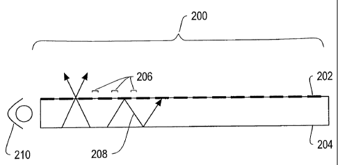
Figure 2 is a cross-section of an optical cavity 200 for use in a spatial
light
modulator, according to an illustrative embodiment of the invention. The
optical
cavity 200 includes a front reflective surface 202 and a rear reflective
surface 204.
CA 02803823 2013-01-30
The front reflective surface 202 includes an array of light-transmissive
regions 206
through which light 208 can escape the optical cavity 200. Light 208 enters
the
optical cavity 200 from one or more light sources 210. The light 206 reflects
between the front and rear reflective surfaces 202 and 204 until it reflects
through
one of the light-transmissive regions 206. Additional reflective surfaces may
be
added along the sides of the optical cavity 200.
The front and rear reflective surfaces 202 and 204, in one implementation,
are formed by depositing a metal or semiconductor onto either a glass or
plastic
substrate. In other implementations, the reflective surfaces 202 and 204 are
formed
by depositing metal or semiconductor on top of a dielectric film that is
deposited as
one of a series of thin films built-up on a substrate. The reflective surfaces
202 and
204 have reflectivities above about 50%. For example, the reflective surfaces
202
and 204 may have reflectivities of 70%, 85%, 96%, or higher.
Smoother substrates and finer grained metals yield higher reflectivities.
Smooth surfaces may be obtained by polishing a glass substrate or by molding
plastic into smooth-walled forms. Alternatively, glass or plastic can be cast
such
that a smooth surface is formed by the settling of a liquid / air interface.
Fine
grained metal films without inclusions can be formed by a number of vapor
deposition techniques including sputtering, evaporation, ion plating, laser
ablation,
or chemical vapor deposition. Metals that are effective for this reflective
application
include, without limitation, Al, Cr, Au, Ag, Cu, Ni, Ta, Ti, Nd, Nb, Si, Mo
and/or
alloys thereof.
Alternatively, the reflective surface can be formed by interposing a
dielectric
material of low refractive index between a light guide in the optical cavity
200 and
any of a series of thin films deposited on top of it. The change in refractive
index
between the light guide and the thin film leads to a condition of total
internal
reflection within the light guide, whereby incident light of sufficiently low
incidence
angle can be reflected with nearly 100% efficiency.
In the alternative, the reflective surfaces 202 or 204 can be formed from a
mirror, such as a dielectric mirror. A dielectric mirror is fabricated as a
stack of
dielectric thin films which alternate between materials of high and low
refractive
16
CA 02803823 2013-01-30
index. A portion of the incident light is reflected from each interface where
the
refractive index changes. By controlling the thickness of the dielectric
layers to
some fixed fraction or multiple of the wavelength and by adding reflections
from
multiple parallel interfaces, it is possible to produce a net reflective
surface having a
reflectivity exceeding 98%. Some dielectric mirrors have reflectivities
greater than
99.8%. Dielectric mirrors can be custom-designed to accept a pre-specified
range of
wavelengths in the visible range and to accept a pre-specified range of
incident
angles. Reflectivities in excess of 99% under these conditions are possible as
long
as the fabricator is able to control the smoothness in the dielectric film
stacks. The
stacks can include between about 20 and about 500 films.
In another alternative, the first and second reflective surfaces 202 or 204
are
included in the optical cavity 200 as separate components. A thin sheet of
polished
stainless steel or aluminum can suffice for this purpose. Also, it is possible
to
produce a reflective metal surface or a dielectric mirror on the surface of a
continuous sheet or roll of plastic. The sheet of reflective plastic can then
be
attached or adhered to other components in the optical cavity 200.
The light-transmissive regions 206 are arranged in an array to form pixels
from which an image is formed. In the illustrative embodiment, the light-
transmissive regions 206 are spaced between about 100 and about 350 microns
apart. The light transmissive regions are oblong or rectangular in shape,
wherein the
greater dimension is between about 50 and about 300 microns while the narrower
dimension is between 2 and 100 microns, though other shapes and sizes may be
suitable. For projection displays the pitch can be as small as 20 microns,
with
aperture widths as small as 5 microns. The ratio between the area of the front
reflective surface 202 taken up by light-transmissive regions 206 and the
total area
of the front reflective surface 202 is referred to herein as the
transmissiveness ratio.
Illustrative implementations of the optical cavity 200 have transmissiveness
ratios of
between about 5% and about 50%. Normally, spatial light modulators having such
low transmissiveness ratios would emit insufficient light to form a usable
image. To
ensure greater light 208 emission from the optical cavity 200, the front and
rear
reflective surfaces 202 and 204 reflect the light 208 back and forth a number
of
times until the reflected light 208 passes through a light-transmissive region
206, or
17
CA 02803823 2013-01-30
until the light 208 loses its energy from the reflections. Higher reflectivity
surfaces
result in more light 208 escaping from the optical cavity 200 to form an
image.
Table 1, below, lists the percentage of light 208 introduced into the optical
cavity
200 that escapes through the light-transmissive regions 206 (in terms of
efficiency)
for several transmissiveness ratio/reflectivity pairings.
Transmissiveness
Ratio Reflectivity Efficiency
0.97 59%
8% 0.93 40%
0.88 30%
0.97 71%
14% 0.93 55%
0.88 43%
0.97 79%
20% 0.93 65%
0.88 53%
TABLE I
When the optical cavity 200 is used to form the basis of a transmissive
display, one or more light sources 210 introduce light into the optical cavity
200.
The light source(s) 210 may be of any suitable type, including, for example,
any of
the types disclosed in U.S. Pat. Nos. 4,897,771 and 5,005,108, the entire
disclosures of which are incorporated herein by reference. In particular, the
light
source(s) 210 may be an arc lamp, an incandescent bulb which also may be
colored,
filtered or painted, a lens end bulb, a line light, a halogen lamp, a light
emitting
diode (LED), a chip from an LED, a neon bulb, a fluorescent tube, a fiber
optic light
pipe transmitting from a remote source, a laser or laser diode, or any other
suitable
light source. Additionally, the light sources may be a multiple colored LED,
or a
combination of multiple colored radiation sources 210 in order to provide a
desired
colored or white light output distribution. For example, a plurality of
colored lights
such as LEDs of different colors (red, blue, green) or a single LED with
multiple
colored chips may be employed to create white light or any other colored light
output distribution by varying the intensities of each individual colored
light. A
reflector may be positioned proximate to the light source 210 to reflect light
208
emitted away from the optical cavity 200 towards the optical cavity 200. In
one
implementation, three light sources 210, one red light source 210, one green
light
source 210, and one blue light source 210, sequentially introduce light 208
into the
18
CA 02803823 2013-01-30
optical cavity 200, alternating at frequencies in the range of 20 to 600 Hz. A
rate in
excess of 100 Hz is generally faster than what the human eye can detect, thus
providing a color image.
Figure 3A is a linear cross-sectional view of a shutter assembly 300 in an
open position. The shutter assembly 300 is formed on transparent substrate 302
having a thickness of from about.3 mm to about 2 mm. The substrate 302 can be,
for example, made of a glass or a plastic. Suitable glasses include
borosilicate
glasses, or other glasses that can withstand processing temperatures up to or
exceeding 400 degrees Centigrade. Suitable plastics for the substrate 302
include,
for example, polyethyleneterephthalate (PET), or polytetrafluoroethylene
(PETF), or
other substantially transparent plastics that can withstand processing
temperatures in
excess of 200 C. Other candidate substrate materials include quartz and
sapphire,
which are understood to withstand processing temperatures in excess of 800 C.
The lowest layer, referred to as the "column metal layer" 304, of the shutter
assembly 300 serves as the front reflective surface 202 of the optical cavity
of
Figure 2. During the process of manufacturing the shutter assembly 300, an
aperture
306 is etched through the column metal layer 304 to form a light-transmissive
region, such as the light transmissive regions 206 of Figure 2. The aperture
306 can
be generally circular, elliptical, polygonal, serpentine, or irregular in
shape. The
aperture occupies about 5% to about 25%of the area dedicated to the particular
shutter assembly 300 in the light modulation array. Other than at the aperture
306,
the column metal layer 304 is substantially unbroken. The aperture 306 is
filled
with a dielectric material 307. Example dielectrics suitable for inclusion in
the
shutter assembly 300 include SiO2, Si3N4, and A12O3.
The next layer is composed mostly of a dielectric material 307, separating
the column metal layer 304 from the row electrodes 308a and 308b disposed a
layer
above. The dielectric layers 316 may be between 0.3 and 10 microns thick. The
top
layer of the shutter assembly 300 includes a shutter anchor 312, two row
anchors
313, two actuators, and a shutter 310. The beams of the actuators are not
shown as
the cross section of the shutter assembly 300 is taken at a position in which
the row
actuator beams meet the row anchors 313 and the shutter actuator beams meet
the
19
CA 02803823 2013-01-30
shutter 310 (see, for example, line B-B' on Figure 1D). The top layer is
supported
above the lower layers by the anchors 312 so that the shutter 310 is free to
move.
In alternative implementations, the row electrodes 308a and 308b are located
at a lower layer in the shutter assembly 300 than the column metal layer 304.
In
another implementation the shutter 310 and actuators can be located at a layer
below either of the column metal layer 304 or the row electrodes 308a and
308b.
As described in relation to Figure 1 B, the actuators included in the shutter
assembly may be designed to be mechanically bi-stable. Alternatively, the
actuators
can be designed to have only one stable position. That is, absent the
application of
some form of actuation force, such actuators return to a predetermined
position,
either open or closed. In such implementations, the shutter assembly 300
includes a
single row electrode 308, which, when energized, causes the actuator to push
or pull
the shutter 310 out of its stable position.
Figure 3B is a cross-sectional view of a second alternative shutter assembly
300' in an open position according to an illustrative embodiment of the
invention.
The second shutter assembly 300' includes a substrate 302', a column metal
layer
304', an aperture 306', row electrodes 308a' and 308b', a shutter 310', two
actuators, a shutter anchor 312', and two row anchors 313'. The beams of the
actuators are not shown as the cross section of the shutter assembly 300' is
taken at a
position in which the row actuator beams meet the row anchors 313' and the
shutter
actuator beams meet the shutter 310'. (See, for example, line B-B' on Figure 1
D).
In the shutter assembly 300', additional gaps are etched into the column
metal layer 304'. The gaps electrically separate different portions of the
column
metal layer 304' such that different voltages can be applied to each portion.
For
instance, in order to reduce parasitic capacitances that can arise between the
column
metal layer 304' and the row electrodes 308a' and 308b' resulting from their
overlap, a voltage can be selectively applied to the sections 314 of the
column metal
layer 304' that immediately underlies the row electrodes 308a' and 308b' and
the
anchor 312'.
Figure 3C is a cross-sectional view of another third alternative shutter
assembly 300" according to an illustrative embodiment of the invention. The
CA 02803823 2013-01-30
shutter assembly 300" includes a substrate 302", a column metal layer 304", an
aperture 306", row electrodes 308a" and 308b", a shutter 310", two actuators,
a
shutter anchor 312", and two row anchors 313". The beams of the actuators are
not
shown as the cross section of the shutter assembly 300" is taken at a position
in
which the row actuator beams meet the row anchors 313" and the shutter
actuator
beams meet the shutter 310". (See, for example, line B-B' on Figure 1 D). The
shutter assembly 300" includes a reflective film 316 deposited on the
substrate
302". The reflective film 316 serves as a front reflective surface for an
optical
cavity incorporating the shutter assembly 300". With the exception of an
aperture
306" formed in the reflective film 316 to provide a light transmissive region,
the
reflective film 316 is substantially unbroken. A dielectric layer 318
separates the
reflective film 316 from the column metal layer 304". At least one additional
dielectric layer 318 separates the column metal layer 304" from the two row
electrodes 308a" and 308b". During the process of the manufacturing of the
third
alternative shutter assembly 300", the column metal layer 304" is etched to
remove
metal located below the row electrodes 308a" and 308b" to reduce potential
capacitances that can form between the row electrodes 308a" and 308b" and the
column metal layer 304". Gaps 320 formed in the column metal layer 304" are
filled in with a dielectric.
Figure 3D is a cross-sectional view of a further alternative shutter assembly
300"' in a closed position according to an illustrative embodiment of the
invention.
The fourth alternative shutter assembly 300"' includes a substrate 302"', a
column
metal layer 304"', an aperture 306"', row electrodes 308a"' and 308b"', a
shutter
310"', two actuators, a shutter anchors 312"', and two row anchors 313"'. The
beams of the actuators are not shown as the cross section of the shutter
assembly
300"' is taken at a position in which the row actuator beams meet the row
anchors
313"' and the shutter actuator beams meet the shutter 310"'. (See, for
example,
line B-B' on Figure 1 D). In contrast to the previously depicted shutter
assemblies
102, 300, 300', and 300", much of the dielectric material used in building the
fourth
alternative shutter assembly 300"' is removed by one or more etching steps.
The space previously occupied by the dielectric material can be filled with a
lubricant to reduce friction and prevent stiction between the moving parts of
the
21
CA 02803823 2013-01-30
shutter assembly 300"'. The lubricant fluid is engineered with viscosities
preferably
below about 10 centipoise and with relative dielectric constant preferably
above
about 2.0, and dielectric breakdown strengths above about 104 V/cm. Such
mechanical and electrical properties are effective at reducing the voltage
necessary
for moving the shutter between open and closed positions. . In one
implementation,
the lubricant preferably has a low refractive index, preferably less than
about 1.5. In
another implementation the lubricant has a refractive index that matches that
of the
substrate 302. Suitable lubricants include, without limitation, de-ionized
water,
methanol, ethanol, silicone oils, fluorinated silicone oils, dimethylsiloxane,
polydimethylsiloxane, hexamethyldisiloxane, and diethylbenzene.
Figure 4 is a cross sectional view of a shutter assembly 400 with a coated
shutter 402, according to an illustrative embodiment of the invention. The
shutter
assembly 400 is depicted as having the general structure of the shutter
assembly 300
of Figure 3A. However, the shutter assembly 400 can take the form of any of
the
shutter assemblies 102, 300, 300', 300", or 300"' described above or any other
shutter assembly described below.
A reflective film 404 coats the bottom of the shutter 402 to reflect light 406
back through the shutter assembly 400 when the shutter 402 is in the closed
position.
Suitable reflective films 404 include, without limitation, smooth depositions
of Al,
Cr, or Ni. The deposition of such a film 404, if the film 404 is greater than
about 0.2
microns thick, provides a reflectivity for the shutter of 95% or higher.
Alternatively,
amorphous or polycrystalline Si, when deposited onto a smooth dielectric
surface,
can provide reflectivity high enough to be useful in this application
The top of the shutter 402 is coated with a light absorbing film 408 to reduce
reflection of ambient light 410 striking the top of the shutter assembly 400.
The
light absorbing film 408 can be formed from the deposition and/or anodization
of a
number of metals, such as Cr, Ni, or Au or Si in a manner that creates a rough
or
porous surface. Alternatively, the light absorbing film 408 can include an
acrylic or
vinyl resin which includes light absorbing pigments. In alternative
implementations
of the shutter assembly 400, the absorbing film 408 is applied to the entire,
or
substantially the entire top surface of the shutter assembly 400.
22
CA 02803823 2013-01-30
Figure 5 is a cross sectional view of a shutter assembly 500 with a second
coated shutter 502, according to an illustrative embodiment of the invention.
The
shutter assembly 500 is depicted as having the general structure of the first
alternative shutter assembly 300 of Figure 3A. However, the shutter assembly
can
take the form of any of the shutter assemblies describes above 102, 300, 300',
300",
and 300"' or any other shutter assembly described below. In the shutter
assembly
500, both the top and the bottom of the shutter 502 are coated with a light
absorbing
film 504 such as a light absorbing film 408. The light absorbing film 504 on
the
bottom of the shutter 502 absorbs light impacting the shutter 502 in a closed
position. For an optical cavity, such as optical cavity 200 of Figure 2,
including the
shutter assembly 500, the intensity of light exiting the optical cavity is
independent
of the image being formed. That is, light intensity is independent of the
fraction of
shutters that may be in the open or the closed position.
Figure 6 is cross-sectional view of an elastically actuated shutter assembly
600 for use in a light modulation array, such as light modulation array 102,
according to an illustrative embodiment of the invention. The elastically
actuated
shutter assembly 600 includes a metal column layer 602, a single row electrode
604,
an elastic element 606, and a shutter 608. The elastic element 606 provides a
restoring force which keeps the shutter 608 in an open position, away from a
corresponding aperture 610 in the column metal layer 602. In the open
position,
light 612 can pass through the aperture 610. Provision of a switching voltage
to the
single row electrode 604 counters the force of the elastic element 606,
thereby
putting the shutter 608 into a closed position over the aperture 610. In the
closed
position, the shutter 608 blocks light 612 from exiting through the aperture
610. In
an alternative implementation, the shutter assembly 600 may include a latch to
lock
the shutter 608 into a closed position such that after the shutter 608 closes,
the row
electrode 604 can be de-energized without the shutter 608 opening. To open the
shutter 608, the latch is released. In still another implementation of the
shutter
assembly 600, the elastic actuator tends to keep the shutter 608 in a closed
position.
Applying a voltage to the row electrode 604 moves the shutter 608 into an open
position.
23
CA 02803823 2013-01-30
Figure 7 is a cross-sectional view of a shutter assembly 700 with a
deformable shutter 701 for use in a light modulation array, according to an
illustrative embodiment of the invention. The shutter assembly 700 includes a
column metal layer 702, and one row electrode 704 formed on a substrate 708.
The
deforming shutter 701, instead of translating from one side of the shutter
assembly
700 to the other side of the shutter assembly 700 to open and close, deforms
in
response to the energizing of the row electrode 704. The deforming shutter 701
is
formed such that the deforming shutter 701 retains residual stress, resulting
in the
deforming shutter 701 tending to curl up out of the plane of the light
modulation
array in which it is included. By imposing a switching voltage between the row
electrode 704 and the column metal layer 702, the deforming shutter 701 is
attracted
towards the substrate 708, thereby covering an aperture 710 formed in the
column
metal layer 702. Deformable or hinge type actuators have been described in the
art,
for instance in U.S. Patent Nos. 4,564,836 and 6,731,492.
Figure 8A is a cross-sectional view of a shutter assembly 800 with an
opaque substrate 802, such as silicon, for use in a light modulation array,
according
to an illustrative embodiment of the invention. The opaque substrate 802 has a
thickness in the range of about 200 microns to about 1 mm. Though the shutter
assembly 800 resembles the shutter assembly 300 of Figure 3A, the shutter
assembly
800 can take substantially the same form of any of the shutter assemblies 300,
300',
300", 300"', 400, 500, 600, or 700 described in Figures 3-7. An aperture 804
is
etched through the entirety of the opaque substrate 802. In one
implementation, the
aperture 804 is formed using an anisotropic dry etch such as in a CFC13 gas
with
plasma or ion assist. The shutter assembly 800 may also include a reflective
coating 810 deposited on the side of the opaque substrate 802 opposite the
column
metal layer.
Figure 8B is a cross-sectional view of a second shutter assembly 800' with
an opaque substrate 802' for use in a light modulation array, according to an
illustrative embodiment of the invention. In comparison to the shutter
assembly 800
in Figure 8A, the underside of the opaque substrate 800' is etched away
forming
cavities 806 beneath the apertures 804' of the shutter assembly 800'. The
cavities
24
CA 02803823 2013-01-30
806 allow light from a larger range of angles to escape through the aperture
804'.
The larger range provides for a brighter image and a larger viewing angle.
The shutter assemblies described in Figures 1 and 3-8 depend on
electrostatic forces for actuation. A number of alternative actuator forcing
mechanisms can be designed into shutter assemblies, including without
limitation
the use of electromagnetic actuators, thermoelastic actuators, piezoelectric
actuators,
and electrostiction actuators. Other shutter motions which can be used to
controllably obstruct an aperture include without limitation sliding,
rotating,
bending, pivoting, hinging, or flapping; all motions which are either within
the plane
of the reflective surface or transverse to that plane.
Figure 9 is a cross-sectional view of a liquid crystal-based spatial light
modulator 900. The liquid crystal-based spatial light modulator 900 includes
an
array 901 of liquid crystal cells 902. The liquid crystal cells 902 include
pairs of
opposing transparent electrodes 904 on either side of a layer of liquid
crystal
molecules 906. On one side of the liquid crystal array 901, the liquid crystal-
based
spatial light modulator 900 includes a polarizer 908. On the opposite side of
the
array 901, the liquid crystal-based spatial light modulator 900 includes an
analyzer
910. Thus, without intervention, light passing through the polarizer 908 would
be
filtered blocked by the analyzer 910. When a voltage is imposed between the
transparent electrodes 904, the liquid crystal molecules 906 between the
electrodes
904 align themselves with the resultant electric field reorienting the light
passing
through the polarizer 908 such that it can pass through the analyzer 910. The
polarizer 908 is positioned on top of a front reflective surface 911, which
defines a
plurality of light-transmission regions 913. The array 901 is attached to an
optical
cavity, such as optical cavity 200 and includes a cover plate 912. Cover
plates are
described in further detail in relation to Figure 11.
Each liquid crystal cell 902 may have a corresponding red, green, or blue
color specific filter. Alternatively, color differentiation can be provided by
multiple
lamps operating in sequence as described above in relation to Figure 2.
Most liquid crystal displays (LCDs) are designed with resolutions of 80 to
110 dots per inch, wherein pixel widths are in the range of 250 to 330
microns. For
CA 02803823 2013-01-30
such an LCD display, even with active matrix or thin-film transistor (TFT)
addressing or switching, the transmissiveness ratio of the liquid-crystal
display is in
the range of 75 to 90%. For high-resolution applications (e.g. for document
displays or projection displays) in which the desired image resolution is 300
to 500
dots per inch, however, and where pixels are only 50 microns in diameter, the
overhead required for TFT addressing can limit the available transmissiveness
ratio
to about 30 or 50%. Such high-resolution displays, therefore, typically suffer
from a
lower luminous efficiency than their lower-resolution counterparts due to a
loss of
aperture ratio. By constructing the liquid crystal display using an optical
cavity as
described above, greater luminous efficiency can be achieved even in high-
definition
LCD displays.
Figure 10 is a cross sectional view of a first shutter-based spatial light
modulator 1000 according to an illustrative embodiment of the invention. The
shutter-based spatial light modulator 1000 includes a light modulation array
1002,
an optical cavity 1004, and a light source 1006. The light modulation array
1002
can include any of the shutter assemblies 300, 300', 300", 300"', 400, 500,
600,
700, 800, or 800' described above in Figures 3-8. The optical cavity 1004, in
the
first shutter-based spatial light modulator 1000, is formed from a light guide
1008
having front and rear surfaces. A front reflective surface 1010 is deposited
directly
on the front surface of the light guide 1008 and a second reflective surface
1012 is
deposited directly on the rear surface of the light guide 1008.
The light guide 1008 can be formed from glass or a transparent plastic such
as polycarbonate or polyethylene. The light guide 1008 is about 300 microns to
about 2 mm thick. The light guide 1008 distributes light 1014 introduced into
the
optical cavity 1004 substantially uniformly across the surface of the front
reflective
surface 1010. The light guide 1008 achieves such distribution by means of a
set of
total internal reflections as well as by the judicial placement of light
scattering
elements 1016. The light scattering elements 1016 can be formed in or on the
rear
side of the light guide 1018 to aid in redirecting light 1014 out of the light
guide
1008 and through light-transmissive regions 1019 formed in the front
reflective
surface 1010.
26
CA 02803823 2013-01-30
Figure 11 is a cross sectional view of a second shutter-based spatial light
modulator 1100, according to the illustrative embodiment of the invention. As
with
the first shutter-based spatial light modulator 1000 in Figure 10, the second
shutter-
based spatial light modulator 1100 includes a light modulation array 1102, an
optical
cavity 1104, and a light source 1106. In addition, the second spatial light
modulator
includes a cover plate 1108.
The cover plate 1108 serves several functions, including protecting the light
modulation array 1102 from mechanical and environmental damage. The cover
plate 1108 is a thin transparent plastic, such as polycarbonate, or a glass
sheet. The
cover plate can be coated and patterned with a light absorbing material, also
referred
to as a black matrix 1110. The black matrix can be deposited onto the cover
plate as
a thick film acrylic or vinyl resin that contains light absorbing pigments.
The black matrix 1110 absorbs substantially all incident ambient light 1112
--ambient light is light that originates from outside the spatial light
modulator 1100,
from the vicinity of the viewer -- except in patterned light-transmissive
regions
1114 positioned substantially proximate to light-transmissive regions 1116
formed
in the optical cavity 1104. The black matrix 1110 thereby increases the
contrast of
an image formed by the spatial light modulator 1100. The black matrix 1110 can
also function to absorb light escaping the optical cavity 1104 that may be
emitted, in
a leaky or time-continuous fashion.
In one implementation, color filters, for example, in the form of acrylic or
vinyl resins are deposited on the cover plate 1108. The filters may be
deposited in a
fashion similar to that used to form the black matrix 1110, but instead, the
filters are
patterned over the open apertures light transmissive regions 1116 of the
optical
cavity 1104. The resins can be doped alternately with red, green, or blue
pigments.
The spacing between the light modulation array 1102 and the cover plate
1108 is less than 100 microns, and may be as little as 10 microns or less. The
light
modulation array 1102 and the cover plate 1108 preferably do not touch,
except, in
some cases, at predetermined points, as this may interfere with the operation
of the
light modulation array 1102. The spacing can be maintained by means of
lithographically defined spacers or posts, 2 to 20 microns tall, which are
placed in
27
CA 02803823 2013-01-30
between the individual right modulators in the light modulators array 1102, or
the
spacing can be maintained by a sheet metal spacer inserted around the edges of
the
combined device.
Figure 12A is a cross sectional view of a third shutter-based spatial light
modulator 1200, according to an illustrative embodiment of the invention. The
third
shutter-based spatial light modulator 1200 includes an optical cavity 1202, a
light
source 1204, and a light modulation array 1206. In addition, the third shutter-
based
spatial light modulator 1204 includes a cover plate 1207, such as the cover
plate
1108 described in relation to Figure 11.
The optical cavity 1202, in the third shutter-based spatial light modulator
1200, includes a light guide 1208 and the rear-facing portion of the light
modulation
array 1206. The light modulation array 1206 is formed on its own substrate
1210.
Both the light guide 1208 and the substrate 1210 each have front and rear
sides. The
light modulation array 1206 is formed on the front side of the substrate 1210.
A
front-facing, rear-reflective surface 1212, in the form of a second metal
layer, is
deposited on the rear side of the light guide 1208 to form the second
reflective
surface of the optical cavity 1202. Alternatively, the optical cavity 1202
includes a
third surface located behind and substantially facing the rear side of the
light guide
1208. In such implementations, the front-facing, rear-reflective surface 1212
is
deposited on the third surface facing the front of the spatial light modulator
1200,
instead of directly on the rear side of the light guide 1208. The light guide
1208
includes a plurality of light scattering elements 1209, such as the light
scattering
elements 1016 described in relation to Figure 10. As in Figure 10, the light
scattering elements are distributed in a predetermined pattern on the rear-
facing side
of the light guide 1208 to create a more uniform distribution of light
throughout the
optical cavity.
In one implementation, the light guide 1208 and the substrate 1210 are held
in intimate contact with one another. They are preferably formed of materials
having similar refractive indices so that reflections are avoided at their
interface. In
another implementation small standoffs or spacer materials keep the light
guide
1208 and the substrate 1210 a predetermined distance apart, thereby optically
de-
28
CA 02803823 2013-01-30
coupling the light guide 1208 and substrate 1210 from each other. The spacing
apart
of the light guide 1208 and the substrate 1210 results in an air gap 1213
forming
between the light guide 1208 and the substrate 1210. The air gap promotes
total
internal reflections within the light guide 1208 at its front-facing surface,
thereby
facilitating the distribution of light 1214 within the light guide before one
of the
light scattering elements 1209 causes the light 1214 to be directed toward the
light
modulator array 1206 shutter assembly. Alternatively, the gap between the
light
guide 1208 and the substrate 1210 can be filled by a vacuum, one or more
selected
gasses, or a liquid.
Figure 12B is a cross sectional view of a fourth shutter-based spatial light
modulator 1200', according to an illustrative embodiment of the invention. As
with
the spatial light modulator 1200 of Figure 12A, the fourth spatial light
modulator
1200' includes an optical cavity 1202', a light source 1204', a light
modulation array
1206', and a cover plate 1207', such as the cover plate 1108 described in
relation to
Figure 11. The optical cavity 1202' includes a rear-facing reflective surface
in the
light modulation array 1206', a light guide 1208', and a front-facing rear-
reflective
surface 1212'. As with the third spatial light modulator 1200, the light
modulation
array 1206' of the fourth spatial light modulator 1200' is formed on a
substrate
1210', which is separate from the light guide 1208'.
In the fourth spatial light modulator 1200', the light guide 1208' and the
substrate 1210' are separated by a light diffuser 1218 and a brightness
enhancing
film 1220. The diffuser 1218 helps to randomize the optical angles of
scattered light
1214' to improve uniformity and reduce the formation of ghost images from the
light source 1204 or the light modulation array 1206. In one implementation,
the
brightness enhancement film 1220 includes an array of optical prisms that are
molded into a thin plastic sheet, and which act to funnel light into a narrow
cone of
illumination. The brightness enhancing film 1220 re-directs light leaving the
light
guide 1208' through light-transmissive regions 1222 at an oblique angle
towards the
viewer, thus resulting in an apparent increases in brightness along the
optical axis
for the same input power.
29
CA 02803823 2013-01-30
Figure 12C is a cross sectional view of a fifth shutter-based spatial light
modulator 1200", according to an illustrative embodiment of the invention. As
with
the spatial light modulator 1200 of Figure 12A, the fifth spatial light
modulator
1200" includes an optical cavity 1202", a light source 1204", a light
modulation
array 1206", and a cover plate 1207", such as the cover plate 1108 described
in
relation to Figure 11. The optical cavity 1202" includes a rear-facing
reflective
surface in the light modulation array 1206", a light guide 1208", and a front-
facing
rear-reflective surface 1212". As with the third spatial light modulator 1200,
the
light modulation array 1206" of the fifth spatial light modulator 1200" is
formed on
a substrate 1210", which is separate from the light guide 1208".
In the fifth spatial light modulator 1200", the light guide 1208" and the
substrate 1210" are separated by a microlens array 1224. The microlens array
1224
re-directs light 1214" leaving the light guide 1208" through light-
transmissive
regions 1222' at an oblique angle towards the viewer, thus resulting in an
apparent
increases in brightness for the same input power.
In addition, since the light modulation array 1206" in the fifth shutter-based
spatial light modulator 1200" is formed on its own substrate 1210", separate
from
the light guide 1208", the light guide 1208" can be constructed of a moldable
plastic, without the transition temperature of the plastic limiting the
manufacturing
processes available for constructing the light modulation array 1210". Thus,
the
light guide 1208" can be molded to substantially encapsulate the light source
1204"
used to introduce light 1214" into the optical cavity 1202". The encapsulation
of
the light source 1204" into the light guide 1208" provides improved coupling
of
light 1214" into the light guide 1208". Similarly, scattering elements 1209"
can be
incorporated directly in the mold for the light guide 1208".
Figure 12D is a cross-sectional view of a sixth illustrative embodiment of a
shutter-based light modulation array 1200"'. As with the spatial light
modulator
1200 of Figure 12A, the sixth spatial light modulator 1200"' includes an
optical
cavity 1202"', a light source 1204"', a light modulation array 1206"', and a
cover
plate 1207"', such as the cover plate 1108 described in relation to Figure 11.
The
optical cavity 1202"' includes a rear-facing reflective surface in the light
CA 02803823 2013-01-30
modulation array 1206"', a light guide 1208"', a front-facing rear-reflective
surface
1212"', a diffuser 1218"', and a brightness enhancing film 1220"'.
The space between the light modulation array 1206"' and the cover plate
1207"' is filled with a lubricant 1224, such as the lubricant described in
relation to
Figure 3D. . The cover plate 1207"' is attached to the shutter assembly 1206
with
an epoxy 1225. The epoxy should have a curing temperature preferably below
about
200 C, it should have a coefficient of thermal expansion preferably below
about 50
ppm per degree C and should be moisture resistant. An exemplary epoxy is EPO-
TEK B9021-1, sold by Epoxy Technology, Inc. The epoxy also serves to seal in
the
lubricant 1224.
A sheet metal or molded plastic assembly bracket 1226 holds the cover plate
1207"', the light modulation array 1206"', and the optical cavity 1202"'
together
around the edges. The assembly bracket 1226 is fastened with screws or indent
tabs to add rigidity to the combined device. In some implementations, the
light
source 1204"' is molded in place by an epoxy potting compound.
Figure 13 is a cross-sectional view of a seventh shutter-based spatial light
modulator 1300 according to an illustrative embodiment of the invention. The
seventh shutter-based spatial light modulator 1300 includes a substrate 1302
on
which a light modulation array 1304 is formed, and a light guide 1306. The
light
modulation array 1304 includes a front reflective surface for the optical
cavity 1310
of the spatial light modulator 1300. A reflective material is deposited or
adhered to
the rear side of the light guide to serve as a rear reflective surface 1308.
The rear
side of the light guide 1306 is angled or shaped with respect to the front
side of the
light guide 1308 to promote uniform distribution of light in the light
modulation
array 1304. The rear reflective surface 1308, however, is still partially
facing the
front reflective surface.
Figure 14A is a cross-sectional view of another spatial light modulator 1400,
according to an illustrative embodiment of the invention. The spatial light
modulator 1400 includes a substrate 1402 on which a light modulation array
1404 is
formed. The light modulation array includes a reflective surface serving as a
front
reflective surface 1405 of an optical cavity. The spatial light modulation
1400 also
31
CA 02803823 2013-01-30
includes a rear reflective surface 1406 substantially facing the rear side of
the light
modulation array 1404. A light source 1408 is positioned within the space
formed
between the substrate 1402 on which the light modulation array 1404 is formed
and
the rear reflective surface 1406. The space may also be filled with a
substantially
transparent plastic into which the light source 1408 is embedded.
Figure 14B is a cross-sectional view of another spatial light modulator 1400',
similar to the spatial light modulator 1400 of Figure 14A. The spatial light
modulator 1400' includes a substrate 1402' on which a light modulation array
1404'
is formed. The light modulation array 1404' includes a reflective surface
serving as
a front reflective surface 1405 of an optical cavity. The spatial light
modulation
1400' also includes a rear reflective surface 1406'. The rear reflective
surface
1406' is corrugated, textured, or shaped to promote light distribution in the
optical
cavity formed by the reflective surfaces (i.e., the rear reflective surface
1406' and a
reflective surface incorporated into the light modulation array 1404' of the
spatial
light modulator 1400'.
Figure 15 is a cross-sectional view of another shutter assembly 1500 for use
in a light modulation array, according to an illustrative embodiment of the
invention.
The shutter assembly 1500 includes a metal column layer 1502, two row
electrodes
1504a and 1504b, a shutter 1506, built on a substrate 1509. The shutter
assembly
1500 also includes one or more light scattering elements 1508. As with other
implementations of the shutter assemblies described above, an aperture 1510 is
etched through the column metal layer 1502. The light scattering elements 1510
can
include any change in the shape or geometry of the substrate 1509, such as by
roughening, coating, or treating the surface of the substrate 1509. For
example, the
light scattering elements can include patterned remnants of the column metal
1502
having dimensions of about I to about 5 microns. The light scattering elements
1508 aid in extracting light 1512 trapped in the substrate 1508 due to total
internal
reflection. When such trapped light 1512 strikes one of the scattering
elements
1508, the angle of the light's 1512 path changes. If the angle of the light's
1512
path becomes sufficiently acute, it passes out of the substrate 1509. If the
shutter
1506 is in the open position, the scattered light 1512 can exit the aperture
1510,
and proceed to a viewer as part of an image.
32
CA 02803823 2013-01-30
Figure 16 is a cross sectional view of yet another spatial light modulator
1600 according to an illustrative embodiment of the invention. The spatial
light
modulator 1600 includes a light modulation array 1602 formed on the rear
surface of
a substrate 1604, facing the interior of an optical cavity 1606. The
individual light
modulation elementsl608, such as the shutter assemblies 300, 300', 300",
300"',
400, 500, 600, 700, 800, and 800' described in Figures 3-8 or the liquid-
crystal cells
902 described in Figure 9, making up the light modulation array 1602 are
modified
to reverse the sides of the light modulation elements 1608 that reflect or
absorb light
as compared to what is described with reference to Figures 4 and 5..
The optical cavity 1606 includes both a front reflective surface 1610, a rear
reflective surface 1612, and a light guide 1614. Light is introduced into the
optical
cavity by a light source 1613. The front reflective surface 1610 is disposed
on front-
facing surface of the light guide 1614, providing a substantially continuous
layer of
high reflectivity and also defining light transmissive region 1616. The front
reflective surface 1610 is separated from the light modulation array 1602 by a
transparent gap 1618. The gap 1618 is preferably narrower than width of the
light
transmissive regions 1616, less than, for example, about 100 microns. The gap
1618
may be as narrow as about 10 microns wide, or even narrower.
In one implementation, the gap 1618 is filled with a lubricant 1620, such as
the lubricant described in relation to Figure 3D. The lubricant 1620 may have
a
refractive index that substantially matches that of the light guide 1614 to
facilitate
the extraction of light from the light guide 1614.
The spatial light modulator 1600 can optionally forego a cover plate, since
the shutter assembly is protected by the environment by the substrate 1604. If
a
cover plate is omitted, a black matrix, such as the black matrix 1110 of
Figure 11,
can be applied to the front-facing surface of the substrate 1604.
Figure 17 is a cross-sectional view of a transflective shutter assembly 1700,
according to an illustrative embodiment of the invention, which can be
incorporated
into the spatial light modulators 1000, 1100, 1200, 1300, 1400, and 1500
described
in Figures 10-15. The transfiective shutter assembly 1700 forms images from
both
light 1701 emitted by a light source positioned behind the shutter assembly
1700 and
from ambient light 1703. The transflective shutter assembly 1700 includes a
metal
33
CA 02803823 2013-01-30
column layer 1702, two row electrodes 1704a and 1704b, and a shutter 1706. The
transflective shutter assembly 1700 includes an aperture 1708 etched through
the
column metal layer 1702. Portions of the column metal layer 1702, having
dimensions of from about 1 to about 5 microns, are left on the surface of the
aperture
1708 to serve as transflection elements 1710. A light absorbing film 1712
covers the
top surface of the shutter 1706.
While the shutter is in the closed position, the light absorbing film 1712
absorbs ambient light 1703 impinging on the top surface of the shutter 1706.
While
the shutter 1706 is in the open position as depicted in Figure 17, the
transflective
shutter assembly 1700 contributes to the formation of an image both by
allowing
light 1701 to pass through the transflective shutter assembly originating from
the
dedicated light source and from reflected ambient light 1703. The small size
of the
transflective elements 1710 results in a somewhat random pattern of ambient
light
1703 reflection.
The transflective shutter assembly 1700 is covered with a cover plate 1714,
which includes a black matrix 1716. The black matrix absorbs light, thereby
substantially preventing ambient light 1703 from reflecting back to a viewer
unless
the ambient light 1703 reflects off of an uncovered aperture 1708.
Figure 18 is a cross-sectional view of a second transflective shutter assembly
1800 according to an illustrative embodiment of the invention, which can be
incorporated into the spatial light modulators 1000, 1100, 1200, 1300, 1400,
and
1500 described in Figures 10-15. The transflective shutter assembly 1800
includes
a metal column layer 1802, two row electrodes 1804a and 1804b, and a shutter
1806.
The transflective shutter assembly 1800 includes an aperture 1808 etched
through
the column metal layer 1702. At least one portion of the column metal layer
1802,
having dimensions of from about 5 to about 20 microns, remains on the surface
of
the aperture 1808 to serve as a transflection element 1810. A light absorbing
film
1812 covers the top surface of the shutter 1806. While the shutter is in the
closed
position, the light absorbing film 1812 absorbs ambient light 1803 impinging
on the
top surface of the shutter 1806. While the shutter 1806 is in the open
position, the
transflective element 1810 reflects a portion of ambient light 1803 striking
the
34
CA 02803823 2013-01-30
aperture 1808 back towards a viewer. The larger dimensions of the
transflective
element 1810 in comparison to the transflective elements 1710 yield a a more
specular mode of reflection, such that ambient light originating from behind
the
viewer is substantially reflected directly back to the viewer.
The transflective shutter assembly 1800 is covered with a cover plate 1814,
which includes a black matrix 1816. The black matrix absorbs light, thereby
substantially preventing ambient light 1803 from reflecting back to a viewer
unless
the ambient light 1803 reflects off of an uncovered aperture 1808.
Referring to both Figures 17 and 18, even with the transflective elements
1710 and 1810 positioned in the apertures 1708 and 1808, some portion of the
ambient light 1703 and 1803 passes through the apertures 1708 and 1808 of the
corresponding transflective shutter assemblies 1700 and 1800. When the
transflective shutter assemblies 1700 and 1800 are incorporated into spatial
light
modulators having optical cavities and light sources, as described above, the
ambient
light1703 and 1803 passing through the apertures 1708 and 1808 enters the
optical
cavity and is recycled along with the light introduced by the light source. In
alternative transflective shutter assemblies, the apertures in the column
metal are at
least partially filled with a semi-reflective-semitransmissive material.
Figure 19 is a cross sectional view of a front reflective shutter assembly
1900
according to an illustrative embodiment of the invention. The front reflective
shutter
assembly 1900 can be used in a reflective light modulation array. The front
reflective shutter assembly 1900 reflects ambient light 1902 towards a viewer.
Thus, use of arrays of the front reflective shutter assembly 1900 in spatial
light
modulators obviates the need for a dedicated light source in viewing
environments
having high amounts of ambient light 1902. The front reflective shutter
assembly
1900 can take substantially the same form of the shutter assemblies 300, 300',
300",
300"', 400, 500, 600, 700, 800 or 800' of Figures 3-8. However, instead of the
column metal layer of the shutter assemblies 300, 400, 500, 600, 700, or 800
including an aperture to allow passage of light, the column metal layer
includes a
reflective surface beneath the position of a closed shutter 1904. The front-
most
layer of the reflective shutter assembly 1900, including at least the front
surface of
CA 02803823 2013-01-30
the shutter 1904, is coated in a light absorbing film 1908. Thus, when the
shutter
1904 is closed, light 1902 impinging on the reflective shutter assembly 1900
is
absorbed. When the shutter 1904 is open, at least a fraction of the light 1902
impinging on the reflective shutter assembly 1900 reflects off the exposed
column
metal layer 1910 back towards a viewer. Alternately the column metal layer
1910
can be covered with an absorbing film while the front surface of shutter 1908
can be
covered in a reflective film. In this fashion light is reflected back to the
viewer only
when the shutter is closed.
As with the other shutter assemblies and light modulators described above,
the reflective shutter assembly 1900 can be covered with a coverplate 1910
having a
black matrix 1912 applied thereto. The black matrix 1912 covers portions of
the
cover plate 1910 not opposing the open position of the shutter.
Figure 20 is an isometric view of a spatial light modulator 2000 including
multiple light modulation arrays 2002, according to an illustrative embodiment
of
the invention. The size of several of the light modulation arrays 2002
described
above is limited, somewhat, by the semiconductor manufacturing techniques used
to
construct them. However, light guides 2004 and reflective films 2006 can be
formed
on a significantly larger scale. A spatial light modulator which includes
multiple,
adjacently disposed light modulation arrays 2002, arranged over one or more
light
guides 2004, can generate a larger image, thereby circumventing these
limitations.
As described above, the shutter assemblies in the above-disclosed shutter
assemblies can be controlled by an active matrix. Figure 21A is a conceptual
diagram of an active control matrix 2100 suitable for inclusion in the display
apparatus 100 for addressing an array of pixels 2140 (the "array 2140"). Each
pixel
2101 includes an elastic shutter assembly 2102, such as the shutter assembly
122 of
Figure 1 C, controlled by an actuator 2103. Each pixel also includes an
aperture
layer 2150 that includes aperture holes 2154. Other electrical and mechanical
configurations of shutter assemblies and the circuits that control them can be
employed without departing from the scope of the invention.
The control matrix 2100 is fabricated as a diffused or thin-film-deposited
electrical circuit on the surface of a substrate 2104 on which the shutter
assemblies
36
CA 02803823 2013-01-30
2102 are formed. The control matrix 2100 includes a scan-line interconnect
2106
for each row of pixels 2101 in the control matrix 2100 and a data-interconnect
2108
for each column of pixels 2101 in the control matrix 2100. Each scan-line
interconnect 2106 electrically connects a write-enabling voltage source 2107
to the
pixels 2101 in a corresponding row of pixels 2101. Each data interconnect 2108
electrically connects a data voltage source, ("Vd source") 2109 to the pixels
2101 in
a corresponding column of pixels 2101. In control matrix 2100, the data
voltage Vd
provides the majority of the energy necessary for actuation of the shutter
assemblies
2102. Thus, the data voltage source 2109 also serves as an actuation voltage
source.
Figure 21 B is an isometric view of a portion of the array of pixels 2140
including the control matrix 2100. Referring to Figures 21 A and 21 B, for
each pixel
2101 or for each shutter assembly in the array of pixels 2140, the control
matrix
2100 includes a transistor 2110 and a capacitor 2112. The gate of each
transistor
2110 is electrically connected to the scan-line interconnect 2106 of the row
in the
array 2140 in which the pixel 2101 is located. The source of each transistor
2110 is
electrically connected to its corresponding data interconnect 2108. The
actuators
2103 of each shutter assembly include two electrodes. The drain of each
transistor
2110 is electrically connected in parallel to one electrode of the
corresponding
capacitor 2112 and to the one of the electrodes of the corresponding actuator
2103.
The other electrode of the capacitor 2112 and the other electrode of the
actuator
2103 in shutter assembly 2102 are connected to a common or ground potential.
In operation, to form an image, the control matrix 2100 write-enables each
row in the array 2140 in sequence by applying Vwe to each scan-line
interconnect
2106 in turn. For a write-enabled row, the application of VWe to the gates of
the
transistors 2110 of the pixels 2101 in the row allows the flow of current
through the
data interconnects 2108 through the transistors to apply a potential to the
actuator
2103 of the shutter assembly 2102. While the row is write-enabled, data
voltages Vd
are selectively applied to the data interconnects 2108. In implementations
providing
analog gray scale, the data voltage applied to each data interconnect 2108 is
varied
in relation to the desired brightness of the pixel 2101 located at the
intersection of
the write-enabled scan-line interconnect 2106 and the data interconnect 2108.
In
implementations providing digital control schemes, the data voltage is
selected to be
37
CA 02803823 2013-01-30
either a relatively low magnitude voltage (i.e., a voltage near ground) or to
meet or
exceed Vat (the actuation threshold voltage). In response to the application
of Vat to
a data interconnect 2108, the actuator 2103 in the corresponding shutter
assembly
2102 actuates, opening the shutter in that shutter assembly 2102. The voltage
applied to the data interconnect 2108 remains stored in the capacitor 2112 of
the
pixel 2101 even after the control matrix 2100 ceases to apply V,e to a row. It
is not
necessary, therefore, to wait and hold the voltage Vwe on a row for times long
enough for the shutter assembly 2102 to actuate; such actuation can proceed
after the
write-enabling voltage has been removed from the row. The voltage in the
capacitors 2112 in a row remain substantially stored until an entire video
frame is
written, and in some implementations until new data is written to the row.
In various implementations, shutter assemblies together with their
corresponding actuators, can be made bi-stable. That is, the shutters in the
shutter
assembly can exist in at least two equilibrium positions (e.g. open or closed)
with
little or no power required to hold them in either position. More
particularly, the
shutter assemblies can be mechanically bi-stable. Once the shutter of such a
shutter
assembly is set in position, no electrical energy or holding voltage is
required to
maintain that position. The mechanical stresses on the physical elements of
the
shutter assembly can hold the shutter in place.
Shutter assemblies, together with their corresponding actuators, can also be
made electrically bi-stable. In an electrically bi-stable shutter assembly,
there exists
a range of voltages below the actuation voltage of the shutter assembly, which
if
applied to a closed actuator (with the shutter being either open or closed),
holds the
actuator closed and the shutter in position, even if an opposing force is
exerted on
the shutter. The opposing force may be exerted by a spring, or the opposing
force
may be exerted by an opposing actuator, such as an "open" or "closed"
actuator.
The pixels 2101 of the array 2140 are formed on a substrate 2104. The array
includes an aperture layer 2150, disposed on the substrate, which includes a
set of
aperture holes 2154 for each pixel 2101 in the array 2140. The aperture holes
2154
are aligned with the shutter assemblies 2102 in each pixel.
38
CA 02803823 2013-01-30
The array 2140 can be fabricated in the following sequence of steps. First
the aperture layer 2150 is deposited and patterned onto a transparent
substrate 2104.
Next, the control matrix, including an array of thin film switches or
transistors 2110,
is fabricated on top of the aperture layer 2150 along with capacitors 2112 and
interconnects, such as scan-line interconnect 2106 or data interconnect 2108.
The
processes employed to fabricate the transistors 2110 and capacitors 2112 can
be
typical of those known in the art for manufacturing active matrix arrays for
use in
liquid crystal displays. In the final step, a micro-electro-mechanical (or
MEMS)
shutter assembly is formed on top of the array of thin film switches.
In one simple implementation, the aperture layer 2150 is electrically isolated
by an intervening dielectric layer from the control matrix. The aperture layer
2150
can consist of thin film materials that are process compatible with the active
matrix
to be fabricated above it, but need not electrically connect to that active
matrix. The
aperture holes 2154 can be generally circular, elliptical, polygonal,
serpentine, or
irregular in shape.
In another implementation, the aperture layer 2150 is electrically connected
to the control matrix. This connection can be made by means of a via etched
through an intervening dielectric layer, such that interconnects in the
control matrix
make electrical contact to the aperture layer. If the aperture layer 2150
includes
conducting materials, it can then act as a ground plane or a common
interconnect for
the control matrix.
In other implementations of the display, a separate aperture layer does not
need to be fabricated as a first step in the sequence. The aperture holes may
be
fabricated instead using the same thin film materials and with the same
processing
steps used in the fabrication of active matrices or passive matrices directly
onto glass
substrates, as typically known in the art. Only the mask designs or pixel
layouts
need to be changed to accommodate the formation of aperture holes.
In another implementation, the aperture layer is fabricated as a last step in
the processing sequence. The aperture layer is rigidly attached to the
substrate but
generally suspended above the shutter assembly, leaving room below for the
free
translational motion of the shutter assembly.
39
CA 02803823 2013-01-30
Figures 22-30 relate to additional MEMS-based display apparatuses. In
particular, the MEMS-based shutter assemblies of Figures 22-30 include optical
light concentrators. Figure 22 is an isometric conceptual view of a reflective
display
apparatus A 10 including an array A100 of light modulators (also referred to
as a
"light modulation array Al00"), an array Al50 of light concentrators (also
referred
to as a "light concentration array A150"), according to an illustrative
embodiment of
the invention. The display apparatus A10 can alternatively be formed as a
transflective or transmissive display. Such embodiments are described further
in
relation to Figures 29 and 30. Light modulation array A100 includes a
plurality of
shutter assemblies A102a-102u (generally "shutter assemblies A102") arranged
in
rows and columns (although segmented displays without rows and columns can
also
be employed without departing from the spirit and scope of the invention). In
general, a shutter assembly A102 has two states, open and closed (although
partial
openings can be employed to impart grey scale, for example, as will be
described in
greater detail below). Each shutter assembly A102 includes a shutter A112 for
selectively covering a corresponding exposable surface A114. Shutter
assemblies
A102a-c, A102e-m, and A102p-u are in the open state, exposing their
corresponding
exposable surfaces A114 to light which has passed through the light
concentration
array A 150. Shutter assemblies A 102d, A 102n, and A 102o are in the closed
state,
obstructing light from impacting their corresponding exposable surfaces A 114
passing through light concentration array A150. In general, apparatus AlO
selectively sets the states of shutter assemblies A102 to reflect light beams
originating from an ambient light source A107, on the same side of the array
as the
viewer, back towards surface A 103 for forming image A104 (see, also, Figure
7, for
example). Alternatively, instead of being ambient to the apparatus A 10, light
source
A 107 could be provided as an integrated front light.
In one embodiment of the invention, each shutter assembly A 102 of light
modulation array A100 may correspond to an image pixel A106 in image A104. As
described above, each shutter assembly A102 includes a shutter A112 and an
exposable surface A114. In one implementation, the surface of the shutter A112
facing the light source A107 is reflective, and the exposable surface A114 is
light-
absorbing. To illuminate a pixel, the shutter A112 is at least partially
closed to
CA 02803823 2013-01-30
reflect light towards the surface Al 03. In an alternative implementation the
surface
of the shutter A112 facing the light source A107 absorbs light and the
exposable
surface A114 reflects light. In this implementation, a pixel A106 is brightest
when
the shutter Al 12 is fully open and darkest when the shutter Al 12 is fully
closed.
In alternative implementations, display apparatus A 10 may employ multiple
shutter assemblies A102 for each image pixel A106. For example, the display
apparatus may include three or four color-specific shutter assemblies A102 per
image pixel A106. By selectively opening one or more of the color-specific
shutter
assemblies A102 corresponding to a particular image pixel A106, the display
apparatus can generate a color image pixel A106 in image A104. In another
example, display apparatus A 10 may include shutter assemblies A 102 that may
provide for multiple partially open or closed states per image pixel A106 to
provide
grey scale in image A 104.
Exposable surface Al 14 may be formed in various ways from films,
depositions, or any other suitable materials, or combinations or lack thereof
which
either reflect or absorb light, depending on the desired implementation of the
shutter
assembly A102. Similarly, each shutter Al 12 may be provided with a surface
that
reflects light therefrom or absorbs light therein, such that in conjunction
with its
associated exposable surface Al 14, light is appropriately reflected or
absorbed,
towards the viewer by assembly A 102, as desired. Such materials are described
further in relation to Figure 23. In still other implementations, display
apparatus
A 10 may include other forms of light modulators, such as micromirrors,
filters,
polarizers, liquid crystal modulation cells, interferometric devices, and
other suitable
devices, instead of shutter assemblies A 102 to modulate light to form an
image.
Light concentration array A 150 includes an array of optical elements for
concentrating light onto respective light modulators in the array of light
modulators
A 100 to increase the fraction of ambient light impacting on either the
shutter A 112
or exposable surface Al 14 depending on the position of the shutter Al 12.
Various
types of optical elements may be provided in light concentration array A150,
including reflective light funnels, high numerical aperture lenses, and other
nonimaging optical devices, for example. In the illustrative embodiment shown
in
41
CA 02803823 2013-01-30
Figure 22, light concentration array A150 includes an array of reflective
light
funnels A 152. Each funnel A 152 is associated with a respective shutter
assembly
A102 for concentrating light emitted from ambient light source A107, onto a
particular region of the shutter assembly A 102 corresponding to the funnel A
152.
Each reflective funnel A 152 preferably includes a first optical opening A156
directed towards the surface A103, a second optical opening A154 directed
towards
its associated shutter assembly A 102, and a wall A 158 connecting the first
optical
opening A156 to the second optical opening A154.
The first optical opening A156 is preferably sized to match the size of an
associated pixel A106, and the second optical opening A154 is preferably sized
to
match or to be slightly smaller than the size of the exposable surface A 114
of its
associated shutter assembly A102. Wall A158 is preferably highly reflective
and the
first optical opening A156 is preferably larger than the second optical
opening A154
such that, to the greatest extent possible, beams of ambient light originating
from
ambient light source A107 may enter funnel A152 at first optical opening A156
from a wide range of angles and be reflected through second optical opening
A154
onto a concentrated region of shutter assembly A102. This increases the
fraction of
available image forming light which gets modulated by each shutter assembly A
102,
thereby improving the contrast ratio of display apparatus A 10. Moreover,
funneling
and concentrating an increased fraction of ambient light A 107 onto a
reflective
element or elements of shutter assembly A 102, display apparatus A 10 is able
to
provide an increased brightness and luminous efficiency while eliminating the
need
for a backlight and additional power.
Wall A158 may be straight, curved, CPC (Compound Parabolic Collector)-
shaped or any suitable combination thereof that provides for an optically
efficient
concentration of ambient light A107 and which also yields a high fill factor.
Wall
A158 may be conical or may include multiple sides, depending on the size and
shape
of the funnel's optical openings. Optical openings A154 and A156 may be of
various shapes and sizes without departing from the spirit and scope of the
invention. Optical openings A156 could be hexagonal while optical openings
A154
could be circular, for example. Wall A158 maybe provided with a reflective
42
CA 02803823 2013-01-30
interior surface or with a transparent interior surface and an exterior
reflective
coating (as described in more detail below with respect to Figures 26A-27C).
Figure 23 is a cross-sectional diagram of one of the combined shutter-funnel
assemblies of Figure 22, illustrating additional features of the display
apparatus A 10.
With reference to Figures 22 and 23, display apparatus A10 may also include a
cover sheet A109 and a filter array layer A111 between the viewer and light
concentration array A150. Cover sheet A109 serves several functions, including
protecting the light modulation array A100 from mechanical and environmental
damage. Cover sheet A 109 may be a thin transparent plastic, such as
polycarbonate,
or a glass sheet, for example. In certain embodiments, the cover sheet can be
coated
and patterned with a light absorbing material, also referred to as a black
matrix
A120. The black matrix A120 can be deposited onto the cover sheet A109 as a
thick
film acrylic or vinyl resin that contains light absorbing pigments. Black
matrix
A120 may absorb certain incident ambient light, thereby increasing the
contrast of
the image A104 formed by apparatus AlO. The black matrix A120 can also
function
to absorb light escaping in a leaky or time-continuous fashion. Top surface A
103 of
cover sheet A109 may display image A104 to the viewer.
In one implementation, filter array Al 11, which may be deposited on cover
sheet A109, may include color filters, for example, in the form of acrylic or
vinyl
resins, or thin film dielectrics. The filters may be deposited in a fashion
similar to
that used to form black matrix A 120, but instead, the filters are patterned
over the
first optical openings A156 or the second optical openings A154 of cones A152
of
light concentration array A150 to provide appropriate color filters for color-
specific
shutter assemblies A102. For example, display apparatus A10 may include
multiple
groupings of three or more color-specific shutter assemblies A102 (e.g., a red
shutter
assembly, a green shutter assembly, and a blue shutter assembly; a red
assembly, a
green shutter assembly, and a blue shutter assembly, and a white shutter
assembly; a
cyan shutter assembly, a magenta shutter assembly, and a yellow shutter
assembly,
etc. - although any other numerical and/or color combination of shutter
assemblies
for forming an image pixel may be provided without departing from the spirit
and
scope of the invention), such that each of the sub-pixels associated with the
color-
specific shutter assemblies A102 of a grouping may form an image pixel A106.
43
CA 02803823 2013-01-30
There could be more than three color subpixesl to make up one full image
pixel. By
selectively opening one or more of the color-specific shutter assemblies A 102
in a
grouping corresponding to a particular pixel, display apparatus A 10 can
generate an
image pixel A106 of various colors for image A104.
These color filters can be made in several ways. For example, materials with
selective absorptivity can be patterned onto the surface of the display using
well
known photolithographic techniques, similar to the steps used in fabricating
the
shutters and passive matrix or active matrix components of the control matrix.
Materials with dispersed metals and metal oxides or more generally specific
absorptive materials can be photosensitive and defined like a photoresist.
Alternatively, such absorptive centers can be applied in a thin film form and
subsequently patterned with well known photolithography and etch processes.
Furthermore, thin films based on interference properties of the thin film
layers can
be patterned on the substrate for forming interference filters over the
representative
red, blue, and green pixels, for example. Color filter materials can also be
formed
from organic dyes dispersed in a resin, such as polyvinyl acrylate.
The height, thickness, shape, and diameters of the optical openings of
funnels At 52 can vary according to the materials employed and the
application.
When the height of wall A158 of funnel A152 is small compared to the
difference in
size between optical openings A154 and A156, the slope of wall A158 is
relatively
shallow (i.e., wall A158 is substantially parallel to surface A103), and
funnel A152
generally acts like a retro-reflector by reflecting most of ambient light A107
back
towards the viewer without first concentrating the light onto the reflective
region or
regions of shutter assembly A102. On the other hand, when the height of wall
A158
of funnel A152 is large compared to the difference in size between optical
openings
A154 and A156, the slope of wall A158 is relatively steep (i.e., wall A158 is
substantially perpendicular to surface A103), resulting in a significant loss
of light
intensity due to multiple reflections of beams of ambient light A107 off of
wall
A158. Ina preferred embodiment, the diameter of first optical opening A156 can
range from between 75 and 225 microns, and is preferably 150 microns; the
diameter of second optical opening A154 can range from between 25 and
75 microns, and is preferably 50 microns; and the height of cone A152 can
range
44
CA 02803823 2013-01-30
from between 100 and 300 microns, and is preferably 200 microns, for example,
yielding slopes ranging from about 3.5 to 4.
In addition, a lens array may be provided with lenses A157 for focusing
incoming ambient light into a respective funnel A 152, and thereby onto the
associated shutter assembly A 102, thereby reducing both the number of
reflections
off of wall A158 and the chance of retro-reflection paths (note that no lenses
A157
are shown in Figure 22 for the sake of clarity of the drawing). Lens A157
positioned
at first optical opening A156 of funnel A152 may help direct and concentrate
oblique incident light rays originating from ambient light source A107 into
funnel
A152 and thus onto the reflective region or regions of shutter assembly A102.
Color
filters of array Al 11 may be fixed to the bottom side of lenses Al 57, for
example, as
shown in Figure 23. As shown in Figure 26, the lens and optical funnel
structures
can be formed as one in a single molding process.
Color filtering can also be done at other locations in display apparatus A10.
In addition to within the cover sheet A 109, color filter array A I 11 may be
applied at
the second optical opening A154 of each reflective light funnel A152, for
example.
This embodiment may be especially preferable in the implementation where
funnels
A 152 are filled with a hard transparent optical material (as described below
in more
detail with respect to Figures 26A-27C). Filter array Al 11 may alternatively
be
applied proximal to the reflective region or regions of shutter assembly A102.
Generally, filters Al I 1 of the filter array may be placed anywhere in the
light path
of a given pixel between surface A103 and the reflective surface of the
shutter
assembly A102.
Reflective wall A158 has a reflectivity above about 50%. For example,
reflective wall A158 may have a reflectivity of 70%, 85%,A92%, 96%, or higher.
Smoother substrates and finer grained metals yield higher reflectivities.
Smooth
surfaces may be obtained by molding plastic into smooth-walled forms. Fine
grained metal films without inclusions can be formed by a number of vapor
deposition techniques including sputtering, evaporation, ion plating, laser
ablation,
or chemical vapor deposition. Metals that are effective for this reflective
application
CA 02803823 2013-01-30
include, without limitation, Al, Cr, Au, Ag, Cu, Ni, Ta, Ti, Nd, Nb, Rh, Si,
Mo,
and/or any alloys or combinations thereof.
Alternatively, reflective wall A158 can be formed from a mirror, such as a
dielectric mirror. A dielectric mirror is fabricated as a stack of dielectric
thin films
which alternate between materials of high and low refractive index. A portion
of the
incident light is reflected from each interface where the refractive index
changes.
By controlling the thickness of the dielectric layers to some fixed fraction
or
multiple of the wavelength and by adding reflections from multiple parallel
interfaces, it is possible to produce a net reflective surface having a
reflectivity
exceeding 98%. Some dielectric mirrors have reflectivities greater than 99.8%.
Dielectric mirrors can be custom-designed to accept a pre-specified range of
wavelengths in the visible range and to accept a pre-specified range of
incident
angles. Reflectivities in excess of 99% under these conditions are possible as
long
as the fabricator is able to control the smoothness in the dielectric film
stacks. The
stacks can include between about 20 and about 500 films, for example.
The state of each shutter assembly A102 can be controlled using a passive
matrix addressing scheme. Each shutter assembly A102 may be controlled by a
column electrode A108 and two row electrodes AI IOa (a "row open electrode")
and
Al 10b (a "row close electrode"). In light modulation array A100, all shutter
assemblies A102 in a given column may share a single column electrode A108.
All
shutter assemblies in a row may share a common row open electrode Al IOa and a
common row close electrode Al lOb.
An active matrix addressing scheme, similar to that described above in
relation to Figures 21A and 21B is also possible. Active matrix addressing (in
which pixel and switching voltages are controlled by means of a thin film
transistor
array or an array of metal insulator metal ("MIM") diodes) is useful in
situations in
which the applied voltage must be maintained in a stable fashion throughout
the
period of a video frame. An implementation with active matrix addressing can
be
constructed with only one row electrode per shutter assembly row.
Referring to Figures 22 and 23, shutter assembly A102 is built on a glass,
silicon, or plastic polymer substrate A 116, which is shared with other
shutter
46
CA 02803823 2013-01-30
assemblies A102 of light modulation array A100. Substrate A116 may support as
many as 4,000,000 shutter assemblies, arranged in up to about 2,000 rows and
up to
about 2,000 columns. A plurality of substrates may be arranged in an array for
signage applications, for example.
Light modulation array A100 and its component shutter assemblies A102 are
formed using standard micromachining techniques known in the art, including
lithography; etching techniques, such as wet chemical, dry, and photoresist
removal;
thermal oxidation of silicon; electroplating and electroless plating;
diffusion
processes, such as boron, phosphorus, arsenic, and antimony diffusion; ion
implantation; film deposition, such as evaporation (filament, electron beam,
flash,
and shadowing and step coverage), sputtering, chemical vapor deposition
("CVD"),
epitaxy (vapor phase, liquid phase, and molecular beam), electroplating,
screen
printing, and lamination. See generally, Jaeger, Introduction to
Microelectronic
Fabrication (Addison-Wesley Publishing Co., Reading Mass., 1988); Runyan, et
at.,
Semiconductor Integrated Circuit Processing Technology (Addison-Wesley
Publishing Co., Reading Mass., 1990); Proceedings of the IEEE Micro Electro
Mechanical Systems Conference, 1987-1998; and Rai-Choudhury, ed., Handbook of
Microlithography, Micromachining & Microfabrication (SPIE Optical Engineering
Press, Bellingham, Wash., 1997).
More specifically, multiple layers of material (typically alternating between
metals and dielectrics) may be deposited on top of a substrate forming a
stack. After
one or more layers of material are added to the stack, patterns may be applied
to a
top most layer of the stack marking material either to be removed from, or to
remain
on, the stack. Various etching techniques, including wet and/or dry etches,
may then
be applied to the patterned stack to remove unwanted material. The etch
process
may remove material from one or more layers of the stack based on the
chemistry of
the etch, the layers in the stack, and the amount of time the etch is applied.
The
manufacturing process may include multiple iterations of layering, patterning,
and
etching.
The process may also include a release step. To provide freedom for parts to
move in the resulting device, sacrificial material may be interdisposed in the
stack
47
CA 02803823 2013-01-30
proximate to material that will form moving parts in the completed device. An
etch
or other fugitive phase process removes much of the sacrificial material,
thereby
freeing the parts to move.
After release, the surfaces of the moving shutter may be insulated so that
charge does not transfer between moving parts upon contact. This can be
accomplished by thermal oxidation and/or by conformal chemical vapor
deposition
of an insulator such as A1203, Cr2O3, TiO2, Hf02, V205, Nb2O5, Ta205, SiO2, or
Si3N4, or by depositing similar materials using techniques such as atomic
layer
deposition. The insulated surfaces may be chemically passivated to prevent
problems such as friction between surfaces in contact by chemical conversion
processes such as fluoridation or hydrogenation of the insulated surfaces.
Dual compliant electrode actuators make up one suitable class of actuators
for driving shutters A112 in shutter assemblies A102. It is to be noted that
many
other various types of actuators, including non-dual compliant electrode
actuators,
may be utilized for driving shutters A112 in shutter assemblies A102 without
departing from the spirit and scope of the invention. A dual compliant beam
electrode actuator, in general, is formed from two or more at least partially
compliant beams. At least two of the beams serve as electrodes (also referred
to
herein as "beam electrodes"). In response to applying a voltage across the
beam
electrodes, the beam electrodes are attracted to one another from the
resultant
electrostatic forces. Both beams in a dual compliant beam electrode are, at
least in
part, compliant. That is, at least some portion of each of the beams can flex
and or
bend to aid in the beams being brought together. In some implementations the
compliance is achieved by the inclusion of corrugated flexures or pin joints.
Some
portion of the beams may be substantially rigid or fixed in place. Preferably,
at least
the majority of the length of the beams are compliant.
Dual compliant electrode actuators have advantages over other actuators
known in the art. Electrostatic comb drives are well suited for actuating over
relatively long distances, but can generate only relatively weak forces.
Parallel plate
or parallel beam actuators can generate relatively large forces but require
small gaps
between the parallel plates or beams and therefore only actuate over
relatively small
48
CA 02803823 2013-01-30
distances. R. Legtenberg et. al. (Journal of Microelectromechanical Systems v.
6, p.
257, 1997) demonstrated how the use of curved electrode actuators can generate
relatively large forces and result in relatively large displacements. The
voltages
required to initiate actuation in Legtenberg, however, are still substantial.
As shown
herein such voltages can be reduced by allowing for the movement or flexure of
both electrodes.
In a dual compliant beam electrode actuator-based shutter assembly, a shutter
is coupled to at least one beam of a dual compliant beam electrode actuator.
As one
of the beams in the actuator is pulled towards the other, the pulled beam
moves the
shutter, too. In doing so, the shutter is moved from a first position to a
second
position. In one of the positions, the shutter interacts with light in an
optical path
by, for example, and without limitation, blocking, reflecting, absorbing,
filtering,
polarizing, diffracting, or otherwise altering a property or path of the
light. The
shutter may be coated with a reflective or light absorbing film to improve its
interferential properties The exposable surface Al 14 interacts with the light
in the
optical path by, for example, and without limitation, blocking, reflecting,
absorbing,
filtering, polarizing, diffracting, or otherwise altering a property or path
of the light,
in a fashion that is complimentarty to that of the optical effect provided by
the
shutter. For example, if one is absorbing the other is reflective or if one
polarizes in
one orientation the other surface polarizes in a perpendicular orientation..
Figures 24A and 24B are plane views of a shutter assembly Al 02, in fully
open and closed states, respectively, according to an illustrative embodiment
of the
invention. The shutter assembly Al 02 utilizes a dual compliant beam electrode
actuators for actuation. Referring to Figures 23, 24A, and 24B, shutter
assembly
Al02 modulates light to form an image by controllably moving a shutter Al 12,
which includes two half-obstructing shutter portions Al 12a and Al 12b, in and
out
of an optical path of light between the viewer and exposable surface A114.
Shutter
portions Al 12a and A112b, when closed, substantially obstruct light from
impacting
the exposable surface 114. In one embodiment, instead of the shutter portions
A112a and A112b being of about equal size, one shutter portion Al 12a or AI
12b is
larger than that of the other shutter portion AI 12a or AI 12b, and they can
be
actuated independently. Thus by selectively opening zero, one, or both shutter
49
CA 02803823 2013-01-30
portions A l 12a and A 112, the shutter assembly A 102 can provide for 4
levels of
gray scale (e.g., off, one-third one, two-thirds on, and fully on).
Shutters Al l2a and Al 12b are each formed from a solid, substantially
planar, body Shutters Al 12a and Al 12b can take virtually any shape, either
regular
or irregular, such that in a closed position shutters Al 12a and Al 12b
sufficiently
obstruct the optical path to exposable surface Al 14. In addition, shutters Al
12a and
Al 12b must have a width consistent with the width of the exposable surface,
such
that, in the open position (as depicted in Figure 24A), sufficient light can
be
absorbed or reflected by exposable surface A114 to darken or illuminate a
pixel,
respectively.
As shown in Figures 24A and 24B, each of shutters A l 12a and A 112b
(shutter Al12) couples to an end of each of two load beams A208. A load anchor
A2 10, at the opposite end of each load beam A208 physically connects the load
beam A208 to substrate A122 and electrically connects the load beam A208 to
driver circuitry formed on the substrate. Together, the load beams A208 and
load
anchors A210 serve as a mechanical support for supporting the shutter A112
over
the exposable surface Al 14, formed on the substrate.
The shutter assembly A 102 includes a pair of drive beams A212 and a pair of
drive beams A214, one of each located along either side of each load beam
A210.
Together, the drive beams A212 and A214 and the load beams A2 10 form an
actuator. Drive beams A212 serve as shutter open electrodes and the other
drive
beams A214 serve as shutter close electrodes. Drive anchors A216 and A218
located at the ends of the drive beams A212 and A214 closest to the shutter Al
12
physically and electrically connect each drive beam A212 and A214 to circuitry
formed or the substrate A122. In this embodiment, the other ends and most of
the
lengths of the drive beams A212 and A214 remain unanchored or free to move.
The load beams A208 and the drive beams A212 and A214 are compliant.
That is, they have sufficient flexibility and resiliency such that they can be
bent out
of their unstressed ("rest") position or shape to at least some useful degree,
without
any significant fatigue or fracture. As the load beams A208 and the drive
beams
A212 and A214 are anchored only at one end, the majority of the lengths of the
CA 02803823 2013-01-30
beams A208, A212, and A214 is free to move, bend, flex, or deform in response
to
an applied force. Corrugations (e.g., corrugations A208a on beams A208) may be
provided to overcome axial stress due to foreshortening of the flexure and to
provide
higher deflections at a given voltage, for example.
Display apparatus A10 actuates shutter assembly A102 (i.e., changes the
state of the shutter assembly A 102) by applying an electric potential, from a
controllable voltage source, to drive beams A212 or A214 via their
corresponding
drive anchors A216 or A218, with the load beams A208 being electrically
coupled
to ground or some different potential, resulting in a voltage across the beams
A208,
A212, and A214. The controllable voltage source, such as a passive or active
matrix
array driver, is electrically coupled to load beams A208 via a passive or
active
matrix as described above. The display apparatus Al0 may additionally or
alternatively apply a potential to the load beams A208 via the load anchors A2
10 of
the shutter assembly A 102 to increase the voltage. An electrical potential
difference
between the drive beams A212 or A214 and the load beams A208, regardless of
sign
or ground potential, will generate an electrostatic force between the beams
which
results in shutter movement transverse in the plane of motion.
The tiling or pixel arrangements for shutter assemblies need not be limited to
the constraints of a square array. Dense tiling can also be achieved using
rectangular, rhombohedral, or hexagonal arrays of pixels, for example, all of
which
find applications in video and color imaging displays.
Figure 25 demonstrates a preferred method of tiling shutter assemblies into
an array of pixels to maximize the aperture ratios in dense arrays and
minimize the
drive voltages. Figure 25 depicts a tiling A400 of dual compliant zipper
electrode
actuator-based shutter assemblies A102 that are tiled on the substrate A122 to
form
image pixels A106 from three generally rectangular shutter assemblies A102.
The
three shutter assemblies A 102 of each pixel A 106 may be independently or
collectively controlled.
Preferably shutter assemblies A 102 are packed close together with as little
dead area therebetween as possible to provide an increased fill factor. As
shown in
Figure 25, portions of shutter assemblies A102 can be interleaved with the
gaps
51
CA 02803823 2013-01-30
between portions of neighboring shutter assemblies A102. The interleaved
arrangement of tiling A400 can be mapped onto a square arrangement of rows and
columns, if desired. As shown, a repeating sequence of columns A420a, A420b,
and
A420c may each be associated with sub-pixels having a specifically colored
filter
Al 11 (e.g., red, green, and blue, respectively). Also, two interleaved rows
of shutter
assemblies A102 are included in a single row electrode A430. The interleaving
can
be utilized to provide for hexagonal packing of the pixels A 106.
In other alternate implementations, the display apparatus A102 can include
multiple (for example, between I and 10) with corresponding exposable surfaces
A114 and corresponding shutters Al 12 per image pixel A106. In changing the
state
of such an image pixel A 106, the number of actuators activated can depend on
the
switching voltage that is applied or on the particular combination of row and
column
electrodes that are chosen for receipt of a switching voltage. Implementations
are
also possible in which partial openings of an aperture are made possible in an
analog
fashion by providing switching voltages partway between a minimum and a
maximum switching voltage. These alternative implementations provide an
improved means of generating a spatial grey scale, for example.
Funnels A152 of light concentration array A150 may be micro-molded,
embossed, or investment casted from a very large family of polymers like
acrylics,
imides, and acetates, for example, as well as plastics, glass, or UV curing
epoxies.
Micro-molding may include subtractive techniques, such as photolithography,
and
etching or embossing techniques in which the inverse pattern is made in a hard
material and subsequently aligned with and pressed into a soft material on the
surface that can subsequently be cured or hardened. Alternatively, funnels
A152
may be fabricated, for example, out of photo-imageable material, such as
Novalac or
PMMA or Polyimide amongst many polymers that can be cross-linked, or whose
cross-links can be broken, with the aid of light. See, for example, "Plastic
vs. Glass
Optics: Factors to Consider (part of SPIE 'Precision Plastic Optics' short
course
note)," of November 17, 1998, by Alex Ning, Ph.d.; "Micro Investment Molding:
Method for Creating Injection Molded Hollow Parts," Proceedings of IMECE2005,
of November 5-11, 2005, by Julian M. Lippmann et al.; and "In-Plane, Hollow
52
CA 02803823 2013-01-30
Microneedles Via Polymer Investment Molding, of 2005, by Julian M. Lippmann et
at.
In one embodiment, referring to Figures 26A-26D, an array A150 of funnels
A152 may be formed first by molding solid cones A152 and optional lens
structures
A157 out of polycarbonate, polymethylmethacrylate, silicone based polymers
("PDMS"), or polyimide, or any other suitable material, for example (see,
e.g., Figure 26A). Then a reflective layer may be coated onto the external and
bottom surface of each cone A152 (see, e.g., Figure 26B), preferably from the
underside of array A150, for forming reflective wall A158. Next, the
reflective
layer coated on the bottom of cones A152 is polished off to provide for second
optical opening A154 of each cone (see, e.g., Figure 26C). Optionally,
polycarbonate, polymethylmethacrylate, silicone based polymers ("PDMS"), or
polyimide, or any other suitable material, for example, may be provided as a
backfill
A155 between cones A152 such that they are formed into a single filled sheet
(see,
e.g., Figure 26D). In the embodiment where cones A152, lenses A157, and cover
sheet A109 are all formed in one layer, filter arrays Al 11 may be provided at
second
optical opening A154 of each cone A152, for example.
Alternatively, in another embodiment, referring to Figures 27A-27C, an
array of depressions, in the form of hollow funnels A152 can be formed, for
example, in a sheet A153 of photo-imageable material A155, such as Novalac or
PMMA or Polyimide amongst many polymers, for example (see, e.g., Figure 27A).
Then a reflective material may be coated onto the inside of each depression to
form
reflective wall A158 (see, e.g., Figure 27B). Next, the bottom of the sheet
A153
may be polished off to form an optical opening, the second optical opening
A154, at
the bottom of the hollow funnels A152 (see, e.g., Figure 27C). Finally, and
optionally, polycarbonate, polymethylmethacrylate, silicone based polymers
("PDMS"), or polyimide, or any other suitable material, for example, may be
provided as a backfill A 159 within cones A 152 such that they are formed into
a
single filled sheet (see, e.g., the region surround by dotted lines in Figure
27C). In
an alternative implementation of this method, the depressions are punched
through
the entirety of the sheet A153, preventing reflective material from collecting
at the
53
CA 02803823 2013-01-30
tip of the hollow funnels A152, thereby obviating the need to remove any
material to
form the second optical opening A154.
Figure 28 is a partial isometric cross-sectional diagram, of one of the
combined shutter, funnel, and pixel assemblies of Figure 22, illustrating
additional
features of the display apparatus A 10 when the apparatus is implemented as a
reflective-type display apparatus A 1010, according to an illustrative
embodiment of
the invention. Reflective display apparatus AlOlO can be used with a
reflective
light modulation array including an array of reflective shutter assemblies A
1102.
Reflective shutter assembly Al 102 reflects ambient light (e.g., typical
ambient light
beam A702) originating from ambient light source A 107 towards a viewer
through
filter array layer A ill and cover sheet A 109 (note that portions of layer A
111 and
sheet A109, including lens A157 are not shown in Figure 28 for the sake of
simplicity of the drawing).
Reflective shutter assembly A 1102 can take substantially the same form as
shutter assembly A102 of Figures 22-25. The front-most layer of reflective
shutter
assembly A 1102 facing the viewer, including at least the front surface of
shutters
All 12a and Al 112b, is coated in a light absorbing film Al 152. Thus, when
shutter
A 1112 is closed, light A702 concentrated by funnel A152 on reflective shutter
assembly Al 102 is absorbed by film A1152. When shutter A1112 is at least
partially open (as depicted in Figure 28), at least a fraction of the light
A702
concentrated on reflective shutter assembly Al 102 reflects off an exposed
reflective
surface A1015 (i.e., exposable surface A1114) of layer Al 118 back towards the
viewer through funnel A152 as specular beams A703. Reflective surface A1015
has
a reflectivity above about 50%. For example, reflective surface A1015 may have
a
reflectivity of 70%, 85%, 92%, 96%, or higher. Smoother substrates and finer
grained metals yield higher reflectivities. Smooth surfaces may be obtained by
molding plastic into smooth-walled forms. Fine grained metal films without
inclusions can be formed by a number of vapor deposition techniques including
sputtering, evaporation, ion plating, laser ablation, or chemical vapor
deposition.
Metals that are effective for this reflective application include, without
limitation,
Al, Cr, Au, Ag, Cu, Ni, Ta, Ti, Nd, Nb, Rh, Si, Mo, and/or any alloys or
combinations thereof.
54
CA 02803823 2013-01-30
Alternatively, reflective surface A1015 can be formed from a mirror, such as
a dielectric mirror. A dielectric mirror is fabricated as a stack of
dielectric thin films
which alternate between materials of high and low refractive index. A portion
of the
incident light is reflected from each interface where the refractive index
changes.
By controlling the thickness of the dielectric layers to some fixed fraction
or
multiple of the wavelength and by adding reflections from multiple parallel
interfaces, it is possible to produce a net reflective surface having a
reflectivity
exceeding 98%. Some dielectric mirrors have reflectivities greater than 99.8%.
Dielectric mirrors can be custom-designed to accept a pre-specified range of
wavelengths in the visible range and to accept a pre-specified range of
incident
angles. Reflectivities in excess of 99% under these conditions are possible as
long
as the fabricator is able to control the smoothness in the dielectric film
stacks. The
stacks can include between about 20 and about 500 films, for example.
Alternately
layer A1118 can be covered with an absorptive film while the front surface of
shutter A1112 can be covered in a reflective film. In this fashion, light is
reflected
back to the viewer through funnel A152 only when shutter A1112 is at least
partially
closed.
Reflective surface A1015 may be roughened in order to provide
diffusiveness thereon for combating glare. This roughening can be done by any
one
of several processes, including mechanical, chemical, or deposition processes.
Roughening the reflective surface causes reflected light to be scattered at
various
angles into funnel A152, and thus at various angles towards the viewer as
diffuse
beams A703', thereby creating wider viewing angles and increasing the ratio of
diffuse (Lambertian) to specular reflections.
The absorbing film Al 152 can be formed, for example from a metal film.
Most metal films absorb a certain fraction of light and reflect the rest. Some
metal
alloys which are effective at absorbing light, include, without limitation,
MoCr,
MoW, MoTi, MoTa, TiW, and TiCr. Metal films formed from the above alloys or
simple metals, such as Ni and Cr with rough surfaces can also be effective at
absorbing light. Such films can be produced by sputter deposition in high gas
pressures (sputtering atmospheres in excess of 20 mtorr). Rough metal films
can
also be formed by the liquid spray or plasma spray application of a dispersion
of
CA 02803823 2013-01-30
metal particles, following by a thermal sintering step. A dielectric layer
such as a
dielectric layer A404 is then added to prevent spalling or flaking of the
metal
particles.
Semiconductor materials, such as amorphous or polycrystalline Si, Ge,
CdTe, InGaAs, colloidal graphite (carbon) and alloys such as SiGe are also
effective
at absorbing light. These materials can be deposited in films having
thicknesses in
excess of 500 nm to prevent any transmission of light through the thin film.
Metal
oxides or nitrides can also be effective at absorbing light, including without
limitation CuO, NiO, Cr203, AgO, SnO, ZnO, TiO, Ta205, Mo03, CrN, TiN, or
TaN. The absorption of these oxides or nitrides improves if the oxides are
prepared
or deposited in non-stoichiometric fashion - often by sputtering or
evaporation -
especially if the deposition process results in a deficit of oxygen in the
lattice. As
with semiconductors, the metal oxides should be deposited to thicknesses in
excess
of 500 nm to prevent transmission of light through the film.
A class of materials, called cermets, is also effective at absorbing light.
Cermets are typically composites of small metal particles suspended in an
oxide or
nitride matrix. Examples include Cr particles in a Cr203 matrix or Cr
particles in an
Si02 matrix. Other metal particles suspended in the matrix can be Ni, Ti, Au,
Ag,
Mo, Nb, and carbon. Other matrix materials include Ti02, Ta205, A1203, and
Si3N4.
It is possible to create multi-layer absorbing structures using destructive
interference of light between suitable thin film materials. A typical
implementation
would involve a partially reflecting layer of an oxide or nitride along with a
metal of
suitable reflectivity. The oxide can be a metal oxide e.g. Cr02, Ti02, A1203
or
Si02 or a nitride like Si3N4 and the metal can be suitable metals such as Cr,
Mo, Al,
Ta, Ti. In one implementation, for absorption of light entering from the
substrate a
thin layer, ranging from 10- 500 nm of metal oxide is deposited first on the
surface
of substrate A402 followed by a 10-500 nm thick metal layer. In another
implementation, for absorption of light entering from the direction opposite
of the
substrate, the metal layer is deposited first followed by deposition of the
metal
oxide. In both cases the absorptivity of bi-layer stack can be optimized if
the
56
CA 02803823 2013-01-30
thickness of the oxide layer is chosen to be substantially equal to one
quarter of 0.55
microns divided by the refractive index of the oxide layer.
In another implementation, a metal layer is deposited on a substrate followed
by a suitable oxide layer of calculated thickness. Then, a thin layer of metal
is
deposited on top of the oxide such that the thin metal is only partially
reflecting
(thicknesses less than .02 microns). Partial reflection from the metal layer
will
destructively interfere with the reflection from substrate metal layer and
thereby
produce a black matrix effect. Absorption will be maximized if the thickness
of the
oxide layer is chosen to be substantially equal to one quarter of 0.55 microns
divided
by the refractive index of the oxide layer.
Figure 29 is a partial isometric cross-sectional diagram, of a portion A20 10
of a transflective display, according to an illustration embodiment of the
invention.
Transflective display apparatus A2010 is similar to reflective display
apparatus Al0,
but transfiective display apparatus forms images from a combination of
reflected
ambient light and transmitted light, emitted from an integral back light A105.
Transflective display apparatus A2010 can be used with a transflective light
modulation array including an array of transflective shutter assemblies A2102
to
modulate both light (e.g., typical backlight beam A801) emitted by backlight
A105
and from ambient light (e.g., typical ambient light beam A802) originating
from
ambient light source A 107 towards a viewer through filter array layer A 111
and
cover sheet A 109 to form an image (note that portions of layer A 111 and
sheet
A109, including lens A157 are not shown in Figure 29 for the sake of
simplicity of
the drawing).
Transflective shutter assembly A2102 can take substantially the same form
as shutter assembly A102 of Figures 22-25. However, layer A2118 of assembly
A2102 includes a reflective surface A2015 and one or more transmissive
apertures
A2018 etched through reflective surface A2015 beneath the position of closed
shutter A2112 to collectively form exposable surface A2114. At least one
portion of
reflective surface A2015, having dimensions of from about 2 to about 20
microns,
remains beneath the position of closed shutter A2112. The front-most layer of
transflective shutter assembly A2102 facing the viewer, including at least the
front
57
CA 02803823 2013-01-30
surface of shutters A2112a and A2112b, is coated in a light absorbing film
A2152.
Thus, when shutter A2112 is closed, ambient light A802 concentrated by funnel
A152 onto transflective shutter assembly A2102 is absorbed by film A2152.
Likewise, when shutter assembly A2112 is closed the trasnmissino of light
through
the trasnmissive aperture A2018 in exposable surface A2114 is blocked. When
shutter A2112 is at least partially open (as depicted in Figure 29),
transflective
shutter assembly A2102 contributes to the formation of an image both by
allowing
at least a fraction of backlight-emitted-light A801 to transmit through
transmissive
apertures A2018 in exposable surface A2114 towards the viewer through funnel
A 152 and by allowing at least a fraction of the ambient light A802
concentrated onto
transfiective shutter assembly A2102 to reflect off of the exposed reflective
surface
or surfaces A2015 of exposable surface A2114 back towards the viewer through
funnel A152. The larger the dimensions of the exposed reflective surface or
surfaces A2015 of exposable surface A2114 in comparison to the transmissive
apertures A2018 become, a more specular mode of reflection is yielded, such
that
ambient light originating from ambient light source A 107 is substantially
reflected
directly back to the viewer. However, as described above with respect to
surface
A1015, reflective surface or surfaces A2015 may be roughened in order to
provide
diffusiveness thereon for combating glare and widening viewing angles of the
display A2010.
Even with funnels A 152 designed to concentrate ambient light A802 onto
one or more of exposed reflective surfaces A2015 that are positioned among
transmissive apertures A2018 on exposable surface A2114, some portion of
ambient
light A802 may pass through apertures A2018 of transflective shutter assembly
A2102. When transflective shutter assembly A2102 is incorporated into spatial
light
modulators having optical cavities and light sources, the ambient light A802
passing
through apertures A2018 enters an optical cavity and is recycled along with
the light
A801 introduced by backlight A105. In alternative transflective shutter
assemblies,
the transmissive apertures in the exposable surface are at least partially
filled with a
semi-reflective-semitransmissive material or alternately the entire exposable
area
A2114 con be formed of a semitransmissive semi-reflective material to achieve
the
same net effect as if portions of the areas are defined as reflective and
transmissive.
58
CA 02803823 2013-01-30
Figure 30 is a partial isometric cross-sectional diagram of a portion of
transmissive display apparatus A3010, according to an illustrative embodiment
of
the invention. As with display apparatus A 10 and A2010, transmissive display
apparatus A3010 includes an array of shutter assemblies A3102, and an array of
light concentrators. In contrast to the previously described display apparatus
AlO
and A2010, in display apparatus A3010, the array of light modulators is
positioned
between the array of light concentrators and a viewer. Transmissive shutter
assemblies A3102 modulate light (e.g., typical backlight beam A901) emitted by
a
backlight A105 towards a viewer. Note that color filter layer AI I I and cover
sheet
A109 are not shown in Figure 30 for the sake of simplicity of the drawing. The
filters Al 11 can be located within display apparatus A3010 anywhere between
the
backlight and the front of the display apparatus A3010.
Transmissive shutter assembly A3102 can take substantially the same form
as shutter assembly A102 of Figures 22-25. However, layer A3118 of assembly
A3102 includes a transmissive surface A3018 beneath the position of closed
shutter
A3112 to form exposable surface A3114. The front-most layer of transmissive
shutter assembly A3102 facing the viewer, including at least the front surface
of
shutters A3112a and A3112b, is coated in a light absorbing film A3152. Thus,
when shutter A3112 is closed, ambient light A902 is absorbed by film A3152 and
is
not reflected back towards the viewer. When shutter A3112 is at least
partially open
(as depicted in Figure 30), transmissive shutter assembly A3102 contributes to
the
formation of an image by allowing at least a fraction of backlight beams A901
to
transmit through transmissive surface A3018 (i.e., exposable surface A3114)
towards the viewer. An additional light blocking area can be applied around of
the
transmissive aperture A3114 so that stray light from the backlight cannot get
through the light modulation layer un-modulated.
As shown, funnel A 152 of light concentration array A 150 is provided
between shutter assembly A3102 and backlight A105 to concentrate backlight
beams A901 entering first optical opening A156 and through second optical
opening
A 154 onto the transmissive region (i.e., transmissive surface A3018 of
exposable
surface A3114) of transmissive shutter assembly A3102. Thus, use of arrays of
transmissive shutter assembly A3 102 in display apparatus A3010 with such a
59
CA 02803823 2013-01-30
configuration of funnels A 152 increases the fraction of image forming light
(i.e., backlight beams A901) from backlight A105 that gets concentrated onto
the
modulating surface (i.e., exposable surface A3114) of the display apparatus.
The
array of light funnels A 152 may also serve as a front reflective layer for
the
backlight to provide for light recycling in the backlight, obviating the need
for a
separate reflective layer. The light entering the funnels at angles not
conducive to
making it to the surface A3114 will be reflected back out of the light funnels
into the
backlight for recycling until such time as it reaches an angle conducive to
exit.
It should be noted that, although apparatus and methods for displays utilizing
light concentration arrays of the invention have been described as utilizing
an array
of reflective light funnels (e.g., funnels A 152), the invention also relates
to apparatus
and methods for displays that utilize light concentration arrays of other
types of
optical elements (i.e., not funnels) for" concentrating available image
forming light
onto an array of light modulators to maximize the contrast ratio of the
display. This
may be accomplished, for example, with the previously described display
apparatus
embodiments by replacing each reflective light funnel A152 with a high
numerical f-
number aperture lens. For example, a high aperture lens, similar to lens A157
shown in Figure 23, could be utilized without cones A152 in an array A150,
according to an alternative embodiment of the invention. Also, while many
implementations described herein disclose the utilization of both lens A157
and light
funnels A152, the lens are optional in many implementations.
Those skilled in the art will know or be able to ascertain using no more than
routine experimentation, many equivalents to the embodiments and practices
described herein. Accordingly, it will be understood that the invention is not
to be
limited to the embodiments disclosed herein, but is to be understood from the
following claims, which are to be interpreted as broadly as allowed under the
law.
The invention may be embodied in other specific forms without departing
from the essential characteristics thereof. The forgoing embodiments are
therefore
to be considered in all respects illustrative, rather than limiting of the
invention.